Transcription
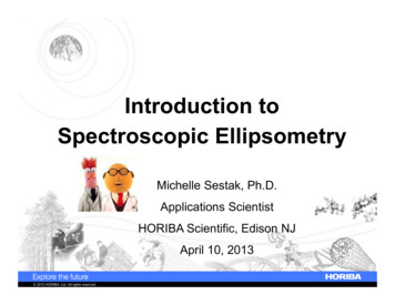
Introduction toSpectroscopic EllipsometryMichelle Sestak, Ph.D.Applications ScientistHORIBA Scientific, Edison NJApril 10, 2013 2007 HORIBA, Ltd. All rights reserved. 2012 HORIBA, Ltd. All rights reserved.
Outline Light and polarization Jones and Stokes vectors Jones and Mueller matrices Optical properties Theory of ellipsometry Methods of SE data collection Instrumentation, with focus on a PME Data analysis Conclusions 20072012 HORIBA,Ltd.All Allrightsreserved.HORIBA,Ltd.rightsreserved.
Ellipsometry Overview Thin Film Applications Non-destructive OpticalTechnique Based on Polarization Change Indirect, Model-based Approach Measure Thickness/OpticalConstants & More! 20072012 HORIBA,Ltd.All Allrightsreserved.HORIBA,Ltd.rightsreserved.
LightxElectric field E(z,t)zDirection ofpropagationyMagnetic field B(z,t) E ( z, t ) E0 x cos( t kz x ) xˆ E0 y cos( t kz y ) yˆEnergy (eV ) h 20072012 HORIBA,Ltd.All Allrightsreserved.HORIBA,Ltd.rightsreserved.hc
Electromagnetic Spectrum1240eV nmE(eV ) h (nm) 20072012 HORIBA,Ltd.All Allrightsreserved.HORIBA,Ltd.rightsreserved.
Polarization Defined by orientation and phase of E-field vector Superposition of two orthogonal wavesXWave 1, ExYWave 2, EyZ 20072012 HORIBA,Ltd.All Allrightsreserved.HORIBA,Ltd.rightsreserved.
Linear Polarization Waves in phase Arbitrary amplitudes 20072012 HORIBA,Ltd.All Allrightsreserved.HORIBA,Ltd.rightsreserved.
Circular Polarization Waves 90º out of phase Equal amplitudes 20072012 HORIBA,Ltd.All Allrightsreserved.HORIBA,Ltd.rightsreserved.
Elliptical PolarizationMost general description of polarization state Arbitrary phase Arbitrary amplitudes 20072012 HORIBA,Ltd.All Allrightsreserved.HORIBA,Ltd.rightsreserved.
Ellipse CharacterizationEyErsE0x x- y rp- rs E0y ExE0 x rptan E0 yrs x y rp rs 20072012 HORIBA,Ltd.All Allrightsreserved.HORIBA,Ltd.rightsreserved. rp rs Erp
Ellipsometry and Polarization Measures changes in polarization state of light Difference in phase shift ( ) Ratio of amplitude change ( ) 20072012 HORIBA,Ltd.All Allrightsreserved.HORIBA,Ltd.rightsreserved.
Ellipsometry vs. Reflectometry Based on IntensityI E2I0Ir Based on amplitude andphase shift of E field;polarization!EinItTransmission It / IoReflection Ir / Io 20072012 HORIBA,Ltd.All Allrightsreserved.HORIBA,Ltd.rightsreserved.rp tan e j rsEout
Ellipsometry Vs Reflectivity Phase ( ) information muchmore sensitive to ultra-thin films35.00030.00025.000¶ (ß)20.00015.0001 nm10.0002 nmNative SiO2 on c-Si0.6500.400170.000160.000150.000140.000 (ß)130.000120.000110.0000.350100.0000.6000.550R 0.5000.4501234Photon Energy (eV)5612345Photon Energy (eV)612345Photon Energy (eV)6Simulation @ 70 AOI 20072012 HORIBA,Ltd.All Allrightsreserved.HORIBA,Ltd.rightsreserved.
Mathematics of Ellipsometry An optical element will change the polarizationstate of light, but how? Jones Vectors and Jones Matrices Completely (pure) polarized light Isotropic sample Stokes Vectors and Mueller Matrices Any polarization state Isotropic or Anisotropic sample 20072012 HORIBA,Ltd.All Allrightsreserved.HORIBA,Ltd.rightsreserved.
Jones Vectors Describe pure polarization states of light E ( z, t ) E0 x cos( t kz x ) xˆ E0 y cos( t kz y ) yˆ J 1Ex E y2 20072012 HORIBA,Ltd.All Allrightsreserved.HORIBA,Ltd.rightsreserved.i x2 Ex e i y Ey e
Jones Vector Examples Linear with x-axis as line ofvibration: 1 0 Linear with y-axis as line ofvibration: 0 1 20072012 HORIBA,Ltd.All Allrightsreserved.HORIBA,Ltd.rightsreserved. Linear polarization oriented at45º:1 1 2 1 Right ( ) and Left Circular (-):1 1 2 i
Jones Vector Examples (cont’d) Elliptical: Unpolarized: DNE tan ei 1 E0 xtan E0 y 20072012 HORIBA,Ltd.All Allrightsreserved.HORIBA,Ltd.rightsreserved. x y
Jones Matrices Polarizer and Analyzer: 1 0 0 0 Photoelastic Modulator:0 1 i ( t ) 0 e 20072012 HORIBA,Ltd.All Allrightsreserved.HORIBA,Ltd.rightsreserved. Isotropic Sample: tan ei 0 0 rp 1 0 Rotation BetweenCoordinates: cos sin sin cos 0 rs
Single Interface: Jones Vectors/Matrices Ei Ei Er Erps r 0 Er E rpsp r r 0 Ei rs E iFor isotropic reflecting surface: rps rsp 0 20072012 HORIBA,Ltd.All Allrightsreserved.HORIBA,Ltd.rightsreserved.ppss rpi tan e rsps
Light Propagation: Jones Matrices Track changes in polarizationLight sourceDetectorPolarizerModulatorAnalyzerSample tan ei 1 0 1 0 R( A) R ( M ) R( M ) E (t ) i 0 0 0 e 0Analyzer 20072012 HORIBA,Ltd.All torSample0 1 0 1 R( P ) 1 0 0 0 PolarizerInitial Pol.State
PME Jones FormalismI (t ) E (t ) I I 0 I s sin (t ) I c cos (t ) 2I 0 1 cos 2 cos 2 A cos 2( P M ) cos 2 M (cos 2 A cos 2 ) cos 2( P M ) sin 2 A sin 2 M sin 2 cos 1I s sin 2( P M ) sin 2 A sin 2 sin sin 2 sin I c sin 2( P M ) sin 2 M (cos 2 cos 2 A) sin 2 A cos 2 M sin 2 cos sin 2 cos 20072012 HORIBA,Ltd.All Allrightsreserved.HORIBA,Ltd.rightsreserved.
Stokes Vectors Describe partial (& pure) polarization states(unpolarized, partially polarized) S0 I x I y S1 I x I y S S2I 45o I 45o S I I 3 rc lc S0 and S1 20072012 HORIBA,Ltd.All Allrightsreserved.HORIBA,Ltd.rightsreserved.S2S3
Stokes Vectors (cont’d)P I tpI tp I un S12 S 22 S32 S0S12 S 22 S32I Totally polarized: S12 S 22 S 32 1; P 1 Partially polarized: S 02 S12 S 22 S32 ; P 1 Unpolarized: S12 S 22 S32 0; P 0 20072012 HORIBA,Ltd.All Allrightsreserved.HORIBA,Ltd.rightsreserved.
Stokes Vector Examples Linear with x-axis as 1 line of vibration: 1 Linear oriented at 45º: Linear with y-axis as 1 line of vibration: 1 Right ( ) and Left (-)Circular: 0 0 0 0 20072012 HORIBA,Ltd.All Allrightsreserved.HORIBA,Ltd.rightsreserved. 1 0 1 0 1 0 0 1
Stokes Vector Examples (cont’d) Elliptical (General): Unpolarized: 20072012 HORIBA,Ltd.All Allrightsreserved.HORIBA,Ltd.rightsreserved.1 P cos 2 P sin 2 cos P sin 2 sin 1 0 0 0
Mueller Matrix Non-ideal depolarizing samples Represents effects of optical components or sampleon Stokes vector S0 M 11 S1 M 21 S M 312 S M 3 OUT 41 20072012 HORIBA,Ltd.All Allrightsreserved.HORIBA,Ltd.rightsreserved.M 12M 22M 13M 23M 32M 42M 33M 43M 14 S 0 M 24 S1 M 34 S 2 M 44 S3 IN
Isotropic Sample M 11 M 21M M 31 M 41M 12M 22M 32M 42M 13M 23M 33M 43M 14 1 M 24 N 0M 34 M 44 0 N100Mueller matrix of a c-Si sample acquired by Auto SE 20072012 HORIBA,Ltd.All Allrightsreserved.HORIBA,Ltd.rightsreserved.00C S0 0 S C
Optical Properties Complex refractive index (Ñ) N n ikIncident rayθ1θ1 n refractive indexcPhase velocity nVelocity cIndex n2Velocity n k extinction coefficientLoss of wave energy to the material 20072012 HORIBA,Ltd.All Allrightsreserved.HORIBA,Ltd.rightsreserved.Index n1θ2Refracted ray k 4
Complex Fresnel Coefficients Describe reflection at eachinterface Depend on angle andpolarization direction (p or s) Errp Ei n cos i ni cos t t p nt cos i ni cos t Errs Ei ni cos i nt cos t s ni cos i nt cos t 20072012 HORIBA,Ltd.All Allrightsreserved.HORIBA,Ltd.rightsreserved.nint i tEts
Determination of Optical Propertiesnint i tEtsUse Snell’s Law and invert: nt cos i ni cos t rn cos i ni cos tptan e i trs ni cos i nt cos t n cos n cos itt ini sin i nt sin t2 1/ 2i 1 tan e2 nt ni sin i 1 tan i i 1 tan e 20072012 HORIBA,Ltd.All Allrightsreserved.HORIBA,Ltd.rightsreserved.
Optical Interference Total reflection coefficientrtot r012 t 01 r12 t10 e -2i t 01 r12 r10 t10 e - 4i r012θ0r01 n0 n1Film2t01r12t10 t01r12r10r12t10dθ1 n2t01t12t01r12r10t12 t01r12r10r12r10t12Substratet012 20072012 HORIBA,Ltd.All Allrightsreserved.HORIBA,Ltd.rightsreserved. . Infinite series solutionsr01 r12 e 2jβR p,s 1 r01r12 e 2jβFilm phase thickness d β 2π n1cos 1 λ
Information from SE Ellipsometry provides information about: Film thicknessOptical propertiesSurface roughnessInterfacial tionUniformity by both depth and area 20072012 HORIBA,Ltd.All eFilmInterfaceSubstrate
Methods of SE Data Collection ex-situ Spectroscopic EllipsometryUVISELUVISEL 2 20072012 HORIBA,Ltd.All SEAUTO-SE
Methods of SE Data Collection (cont’d) in-situ Spectroscopic Ellipsometry Nucleation parametersFilm growth modesOptical properties w/o oxideFilm growth profiles 20072012 HORIBA,Ltd.All Allrightsreserved.HORIBA,Ltd.rightsreserved.
Methods of SE Data Collection (cont’d) Mapping2-D Wafer Plot2-D Point Values3-D Wafer Map 20072012 HORIBA,Ltd.All Allrightsreserved.HORIBA,Ltd.rightsreserved.
Methods of SE Data Collection (cont’d) In-line 20072012 HORIBA,Ltd.All Allrightsreserved.HORIBA,Ltd.rightsreserved.
Methods of SE Data Collection (cont’d) Vacuum Ultraviolet (VUV) Spectral Range of 147-850 nm (NIR option to 2100 nm) Remove absorption at low wavelengths due to O2 20072012 HORIBA,Ltd.All Allrightsreserved.HORIBA,Ltd.rightsreserved.
Methods of SE Data Collection (cont’d) Reflectometry/Transmission Temperature controlled 20072012 HORIBA,Ltd.All Allrightsreserved.HORIBA,Ltd.rightsreserved.
Methods of SE Data Collection (cont’d) Liquid Cell Sealed Cell 20072012 HORIBA,Ltd.All Allrightsreserved.HORIBA,Ltd.rightsreserved. Electrochemical Cell
Methods of SE Data Collection (cont’d) Textured SamplesSEM picture of textured c-Si 20072012 HORIBA,Ltd.All Allrightsreserved.HORIBA,Ltd.rightsreserved.
Ellipsometry Advantages Non-destructive, non-invasive, and non-contact Precise and reproducible Very sensitive to ultra-thin films 10 nm Applicable to almost any thin film materials(polymers, semiconductors, dielectrics, metals,alloys, etc.) Ideal for in-situ applications 20072012 HORIBA,Ltd.All Allrightsreserved.HORIBA,Ltd.rightsreserved.
InstrumentationRotating AnalyzerPSARotating CompensatorPCSAPhase ModulationPSMALiquid Crystal Phase ModulationP 20072012 HORIBA,Ltd.All DetectorLight SourceP: PolarizerA: AnalyzerC: CompensatorS: SampleM: ModulatorLC: LiquidCrystal
Phase Modulated Hz)Fixed PolarizerHORIBA UVISEL 2Optical FiberDetectorSampleMonochromator 20072012 HORIBA,Ltd.All rData Acquisitionand ComputerXe lamp(DeltaPsi2)
Photoelastic Modulator PrincipleAn electrically driven retarder introducing a phase shift varying sinusoidally with timeLinearly polarized lightExn0modulatorn1dPiezo electric transducer (50 kHz) Signal detected at 50 kHz !!!Elliptically polarized light Strained SiO2 bar; birefringence Modulation at 50 kHz! 20072012 HORIBA,Ltd.All i Ey
PME Advantages Fixed elements Excellent precision on Very fast acquisition rate ( 1 ms/point) Covers a wide spectral range from 190-2100 nm High polarization modulation rate of 50 kHz Ψ and are measured over their full range; Ψ[0 , 90 ] and [0 , 360 ] 20072012 HORIBA,Ltd.All Allrightsreserved.HORIBA,Ltd.rightsreserved.
SE Data AnalysisUse Regression AnalysisMeasurementModelFit300150100502.5E 00Optical Constants250200150Delta ( )200Psi ( )Layer 1250Delta ( )Psi ( )Layer 23502ThicknessEXPERIMENTAL DATAEXPERIMENTAL DATA191817161514131211109876541.5ResultsRoughness 1005022.5E (eV)3(n,k) f(lambda) for the TiO2 0.152.50.12.40.052.3400 20072012 HORIBA,Ltd.All ex)Re(Index)3500600lambda (nm)7008000
Data Fitting Goodness of fit:2( XExp - XTh )1 22N - P - 1 N 2N: Total number of measurablesP: Total number of fit parametersIn phase modulated ellipsometry X represents the couple (Is, Ic) 20072012 HORIBA,Ltd.All Allrightsreserved.HORIBA,Ltd.rightsreserved.
Kramers-Kronig (KK) Transformation Real and imaginary terms of optical propertiesare not independent! 1 1 2 2 2 P 2 d 22 0P 0 1 1 d 2 2 1 n 2 k 2 2 2nk 20072012 HORIBA,Ltd.All Allrightsreserved.HORIBA,Ltd.rightsreserved.
Implications of KK Relationship Refractive index (n): Always follows slope of k Always increasing for absorbing materials,except in regions of anomalous 0.4n 50350 20072012 HORIBA,Ltd.All 500550600Wavelength (nm)650700750800
Normal Dispersion: Dielectric Refractive index (n) decreases with increasing λ43AlGaAsn2SiNxSiO21400 420 440 460 480 500 520 540 560 580 600 620 640 660 680 700 720 740 760 780 800Wavelength (nm) 20072012 HORIBA,Ltd.All Allrightsreserved.HORIBA,Ltd.rightsreserved.
Anomalous Dispersion: Absorbing Region Refractive index (n) increases with increasing λexcept where absorption peak occurs0.73.150.653.10.63.050.5530.52.950.452.90.4n 50350 20072012 HORIBA,Ltd.All 500550600Wavelength (nm)650700750800
Quality of Results Goal: find simplest, realistic model Minimize Are results physical? Negative k? K-K consistent? Follow anomalous or normal dispersion? Other indicators Error bars (90% confidence limits) Correlation matrix 20072012 HORIBA,Ltd.All Allrightsreserved.HORIBA,Ltd.rightsreserved.
Applications-Thin FilmsAt home: entertainment, comfort,security, appliances, energy savings Our health:In the car:medical imaging,portable diagnostics,DNA analysis,implantabledevices engine control andpowertrain, car body andsafety, navigation.On the go:At work:mobile phones, PDAs,MP3 players, tablets printers, PCs, Our planet: energy-savingsolutions, solar power, greener cars 20072012 HORIBA,Ltd.All Allrightsreserved.HORIBA,Ltd.rightsreserved.
Thin Films in PhotovoltaicsStructure Si: crystalline, nano, micro, poly,amorphous, textured. Compound semiconductor: III-V,SiGe, CdTe, CIS, CIGS. Organics: PCBM, P3HT,PEDOT:PSS. Transparent conducting oxides(TCO): SnO2, ZnO, ITO. AR coating: SiNx, TiOx Metal contacts: Al, Ca, Mg 20072012 HORIBA,Ltd.All rAbsorber
Thin Films in Displays Devices: TFT-LCD LED, OLED Materials: a-Si, Poly-Si,SiN, SiO2,MgO,ITO,SnO2,ZnOLiquid crystals, Antireflection (AR) coatingPolarizing filters 20072012 HORIBA,Ltd.All Allrightsreserved.HORIBA,Ltd.rightsreserved.
Thin Films in Optoelectronics Devices: High sensitivity NIR & IR detectors Laser Diodes (LED) High speed electronics Materials: III-V compoundsII-VI compoundsTernary alloysQuternary alloysMultiquantum well GaN, SiO2 ,TiO2.Vision and microspotcapabilities can be crucial 20072012 HORIBA,Ltd.All Allrightsreserved.HORIBA,Ltd.rightsreserved.
Thin Films in Microelectronics Materials: 20072012 HORIBA,Ltd.All Allrightsreserved.HORIBA,Ltd.rightsreserved.a-Si, Poly-Si,SiN, SiO2,High , Low materialsMaterials for 90 nm lithography ( DUV )New materials : Graphene,Nanomaterials
Thin Films in Optical Coatings Applications: Antireflection coatingFiltering coatingsAntiscratch coatingDecorative coatingsElectrochromic coatings Materials: SiOx, High/Low refractive multilyers SiN,TiOx, WOx, 20072012 HORIBA,Ltd.All Allrightsreserved.HORIBA,Ltd.rightsreserved.
Thin films in Biochemistry Objective: Selective capture of protein Biosensors Materials: Substrate: Gold Layers: DNA, proteins 20072012 HORIBA,Ltd.All Allrightsreserved.HORIBA,Ltd.rightsreserved.
Thin Films in Metallurgy Objective: HardnessAntifriction coatingsDecorative coatingAnticorrosion coating Materials: SiOx, TiO2, Al, Al2O3,CrO2, DLC TiN, 20072012 HORIBA,Ltd.All Allrightsreserved.HORIBA,Ltd.rightsreserved.
Emerging Applications & Materials Objective: Microelectronics, Display& solar cells on flexiblesubstrate Materials : Substrate: PET Layers: Polymers, a-Si Low Cost ProductionLow Power Consumption 20072012 HORIBA,Ltd.All Allrightsreserved.HORIBA,Ltd.rightsreserved.
Summary Optical technique for studying thin film thicknessand optical properties Ellipsometry vs. Reflectometry Jones/Stoke vectors and Jones/Mueller matricesused for light propagation Model based approach Many data collection methods Wide field of applications 20072012 HORIBA,Ltd.All Allrightsreserved.HORIBA,Ltd.rightsreserved.
Thank you!Check our website for future webinarson spectroscopic ellipsometry! 2012 HORIBA, Ltd. All rights reserved.
Questions? For additional information or questions aboutellipsometry, please visit:www.horiba.com/ellipsometry Or email:ellipsometry.us@horiba.com 20072012 HORIBA,Ltd.All Allrightsreserved.HORIBA,Ltd.rightsreserved.
Mathematics of Ellipsometry An optical element will change the polarization state of light, but how? Jones Vectors and Jones Matrices Completely (pure) polarized light Isotropic sample Stokes Vectors and Mueller Matric