Transcription
A Designer’s Guide toInstrumentation Amplifiers3 RD Editionwww.analog.com/inamps
A DESIGNER’S GUIDE TOINSTRUMENTATION AMPLIFIERS3RD EditionbyCharles Kitchin and Lew Counts
All rights reserved. This publication, or parts thereof, may not bereproduced in any form without permission of the copyright owner.Information furnished by Analog Devices, Inc. is believed to beaccurate and reliable. However, no responsibility is assumed byAnalog Devices, Inc. for its use.Analog Devices, Inc. makes no representation that the interconnection of its circuits as described herein will not infringe on existing orfuture patent rights, nor do the descriptions contained herein implythe granting of licenses to make, use, or sell equipment constructedin accordance therewith.Specifications and prices are subject to change without notice. 2006 Analog Devices, Inc. Printed in the U.S.A.G02678-15-9/06(B)ii
TABLE OF CONTENTSCHAPTER I—IN-AMP BASICS . 1-1Introduction . . 1-1IN-AMPS vs. OP AMPS: WHAT ARE THE DIFFERENCES? . 1-1Signal Amplification and Common-Mode Rejection . 1-1Common-Mode Rejection: Op Amp vs. In-Amp . . 1-3Difference Amplifiers . 1-5WHERE are in-amps and Difference amps used? . 1-5Data Acquisition . 1-5Medical Instrumentation . 1-6Monitor and Control Electronics . 1-6Software-Programmable Applications . 1-6Audio Applications . . 1-6High Speed Signal Conditioning . . 1-6Video Applications . 1-6Power Control Applications . 1-6IN-AMPS: AN EXTERNAL VIEW . 1-6WHAT OTHER PROPERTIES DEFINE A HIGH QUALITY IN-AMP? . . 1-7High AC (and DC) Common-Mode Rejection . 1-7Low Offset Voltage and Offset Voltage Drift . 1-7A Matched, High Input Impedance . 1-8Low Input Bias and Offset Current Errors . 1-8Low Noise . 1-8Low Nonlinearity . 1-8Simple Gain Selection . 1-8Adequate Bandwidth . . 1-8Differential to Single-Ended Conversion . 1-9Rail-to-Rail Input and Output Swing . 1-9Power vs. Bandwidth, Slew Rate, and Noise . 1-9CHAPTER II—INSIDE AN INSTRUMENTATION AMPLIFIER . . 2-1A Simple Op Amp Subtractor Provides an In-Amp Function . 2-1Improving the Simple Subtractor with Input Buffering . 2-1The 3-Op Amp In-Amp . 2-23-Op Amp In-Amp Design Considerations . . 2-3The Basic 2-Op Amp Instrumentation Amplifier . 2-42-Op Amp In-Amps —Common-Mode Design Considerations for Single-Supply Operation . 2-5CHAPTER III—MONOLITHIC INSTRUMENTATION AMPLIFIERS . 3-1Advantages Over Op Amp In-Amps . 3-1Which to Use—an In-Amp or a Diff Amp? . 3-1MONOLITHIC IN-AMP DESIGN—THE INSIDE STORYHigh Performance In-Amps . . 3-2Low Cost In-Amps . 3-5Pin-Programmable, Precise Gain In-Amps . 3-6Auto-Zeroing Instrumentation Amplifiers. 3-8Fixed Gain (Low Drift) In-Amps . 3-16Monolithic In-Amps Optimized for Single-Supply Operation . 3-17Low Power, Single-Supply In-Amps . . 3-19Gain-Programmable In-Amps . 3-20CHAPTER IV—MONOLITHIC DIFFERENCE AMPLIFIERS . 4-1Difference (Subtractor) Amplifier Products . 4-1AD8205 Difference Amplifier . 4-3iii
Gain Adjustment . . 4-6High Frequency Differential Receiver/Amplifiers . 4-9CHAPTER V—APPLYING IN-AMPS EFFECTIVELY . 5-1Dual-Supply Operation . 5-1Single-Supply Operation . 5-1The Need for True R-R Devices in Low Voltage, Single-Supply IA Circuits . 5-1Power Supply Bypassing, Decoupling, and Stability Issues . 5-1THE IMPORTANCE OF AN INPUT GROUND RETURN . 5-2Providing Adequate Input and Output Swing (“Headroom”) When AC Coupling aSingle-Supply In-Amp . . 5-3Selecting and Matching RC Coupling Components . . 5-3Properly Driving an In-Amp’s Reference Input . . 5-4Cable Termination . 5-5Input Protection Basics For ADI In-Amps . 5-5Input Protection from ESD and DC Overload . . 5-5Adding External Protection Diodes . . 5-8ESD and Transient Overload Protection . . 5-9Design Issues Affecting DC Accuracy . 5-9Designing for the Lowest Possible Offset Voltage Drift . 5-9Designing for the Lowest Possible Gain Drift . 5-9Practical Solutions . 5-11Option 1: Use a Better Quality Gain Resistor . . 5-11Option 2: Use a Fixed-Gain In-Amp . 5-11RTI AND RTO ERRORS . 5-11Offset Error . . 5-12Noise Errors . 5-12Reducing RFI Rectification Errors in In-Amp Circuits . 5-12Designing Practical RFI Filters . 5-12Selecting RFI Input Filter Component Values Using a Cookbook Approach . 5-14Specific Design Examples . . 5-15An RFI Circuit for AD620 Series In-Amps . 5-15An RFI Circuit for Micropower In-Amps . . 5-15An RFI Filter for the AD623 In-Amp . . 5-16AD8225 RFI Filter Circuit . 5-16An RFI Filter For The AD8555 Sensor Amplifier . 5-17In-Amps with On-Chip EMI/RFI Filtering . 5-17Common-Mode Filters Using X2Y Capacitors . 5-19Using Common-Mode RF Chokes for In-Amp RFI Filters . 5-20RFI TESTING . 5-21USING LOW-PASS FILTERING TO IMPROVE SIGNAL-TO-NOISE RATIO . 5-21EXTERNAL CMR AND SETTLING TIME ADJUSTMENTS . . 5-23CHAPTER VI—IN-AMP AND DIFF AMP APPLICATIONS CIRCUITS . 6-1A True Differential Output In-Amp Circuit . 6-1DIFFERENCE AMPLIFIER MEASURES HIGH VOLTAGES . . 6-1Precision Current Source . 6-3Integrator for PID Loop . 6-3Composite In-Amp Circuit Has Excellent High Frequency CMR . 6-3Strain Gage Measurement Using An AC Excitation . 6-5Applications of the AD628 Precision Gain Block . 6-6Why Use a Gain Block IC? . 6-6Standard Differential Input ADC Buffer Circuit with Single-Pole LP Filter . 6-6Changing the Output Scale Factor . . 6-7iv
Using an External Resistor to Operate the AD628 at Gains Below 0.1 . . 6-7Differential Input Circuit with 2-Pole Low-Pass Filtering . 6-8Using the AD628 to Create Precision Gain Blocks . 6-9Operating the AD628 as a 10 or –10 Precision Gain Block . 6-9Operating the AD628 at a Precision Gain of 11 . . 6-10Operating the AD628 at a Precision Gain of 1 . . 6-10Increased BW Gain Block of –9.91 Using Feedforward . . 6-11CURRENT TRANSMITTER REJECTS GROUND NOISE . 6-12High Level ADC Interface . 6-13A High Speed noninverting Summing Amplifier . 6-15High Voltage Monitor . 6-16PRECISION 48 V BUS MONITOR . . 6-17HIGH-SIDE CURRENT SENSE WITH A LOW-SIDE SWITCH . 6-18HIGH-SIDE CURRENT SENSE WITH A HIGH-SIDE SWITCH . 6-19Motor Control . 6-19BRIDGE APPLICATIONS . . 6-19A Classic Bridge Circuit . 6-19A Single-Supply Data Acquisition System . 6-20A Low Dropout Bipolar Bridge Driver . 6-20TRANSDUCER INTERFACE APPLICATIONS . 6-21ELECTROCARDIOGRAM SIGNAL CONDITIONING . 6-21REMOTE LOAD-SENSING TECHNIQUE . . 6-24A PRECISION VOLTAGE-TO-CURRENT CONVERTER . . 6-24A CURRENT SENSOR INTERFACE . 6-24OUTPUT BUFFERING, LOW POWER IN-AMPS . 6-25A 4 TO 20 mA SINGLE-SUPPLY RECEIVER . 6-26A SINGLE-SUPPLY THERMOCOUPLE AMPLIFIER . 6-26SPECIALTY PRODUCTS . 6-26Chapter vii—matching in-amp circuits to modern adcs . . 7-1Calculating ADC Requirements . . 7-1Matching ADI In-Amps with Some Popular ADCs . . 7-2High Speed Data Acquisition . . 7-7A High Speed In-Amp Circuit for Data Acquisition . . 7-8APPENDIX A—INSTRUMENTATION AMPLIFIER SPECIFICATIONS . A-1(A) Specifications (Conditions) . A-3(B) Common-Mode Rejection . A-3(C) AC Common-Mode Rejection . A-3(D) Voltage Offset . . A-3(E) Input Bias and Offset Currents . A-4(F) Operating Voltage Range . A-4(G) Quiescent Supply Current . A-4(H) Settling Time . . A-5(I) Gain . A-5(J) Gain Range . A-5(K) Gain Error . A-5(L) Nonlinearity . A-6(M) Gain vs. Temperature . A-6(N) Key Specifications for Single-Supply In-Amps . A-6Input and Output Voltage Swing . . A-6APPENDIX B—AMPLIFIERS SELECTION TABLE . . B-1INDEX . C-1DEVICE INDEX . D-1
BIBLIOGRAPHY/FURTHER READINGBrokaw, Paul. “An IC Amplifier Users’ Guide to Decoupling, Grounding, and Making Things Go Right for aChange.” Application Note AN-202, Rev. B. Analog Devices, Inc. 2000.Jung, Walter. IC Op Amp Cookbook. 3rd ed. Prentice-Hall PTR. 1986. 1997. ISBN: 0-13-889601-1.This can also be purchased on the Web at http://dogbert.abebooks.com.Jung, Walter. Op Amp Applications Handbook. Elsevier/Newnes. 2006.Jung, Walter. Op Amp Applications. Analog Devices. 2002. These seminar notes are an early version of theOp Amp Applications Handbook. You can download this (Free) on the Web at: ves/39-05/op amp applications handbook.html.Kester, Walt. The Data Conversion Handbook. Elsevier/Newnes. 2005. ISBN: 0-7506-7841-0.Kester, Walt. Mixed-Signal and DSP Design Techniques. Elsevier/Newnes. 2003. ISBN: 0-7506-7611-6.Kester, Walt. Practical Design Techniques for Sensor Signal Conditioning. Analog Devices, Inc. 1999. Section 10.ISBN-0-916550-20-6. Available for download on the ADI website at www.analog.com.Moghimi, Reza. “Bridge-Type Sensor Measurements Are Enhanced by Auto-Zeroed InstrumentationAmplifiers with Digitally Programmable Gain and Offset.” Analog Dialogue. May 3, 2004. ves/38-05/AD8555.html.Nash, Eamon. “Errors and Error Budget Analysis in Instrumentation Amplifier Applications.” ApplicationNote AN-539. Analog Devices, Inc.Nash, Eamon. “A Practical Review of Common-Mode and Instrumentation Amplifiers.” Sensors Magazine.July 1998.Sheingold, Dan, ed. Transducer Interface Handbook. Analog Devices, Inc. 1980. pp. 28-30.Wurcer, Scott and Walter Jung. “Instrumentation Amplifiers Solve Unusual Design Problems.” ApplicationNote AN-245. Applications Reference Manual. Analog Devices, Inc.ACKNOWLEDGMENTSWe gratefully acknowledge the support and assistance of the following: Moshe Gerstenhaber, ScottWurcer, Stephen Lee, Bright Gao, Scott Pavlik, Henri Sino, Alasdair Alexander, Chau Tran, AndrewTang, Tom Botker, Jim Bundock, Sam Weinstein, Chuck Whiting, Matt Duff, Eamon Nash, Walt Kester,Alain Guery, Chris Augusta, Claire Croke, Nicola O’Byrne, James Staley, Ben Doubts, Padraig Cooney,Leslie Vaughan, Edie Kramer, and Lynne Hulme of Analog Devices. Also to David Anthony of X2YTechnology and Steven Weir of Weir Design Engineering, for the detailed applications information onapplying X2Y products for RFI suppression.And finally, a special thank you to Analog Devices’ Communications Services team, including John Galgay,Alex Wong, Terry Gildred, Kirsten Dickerson, and Kelley Moretta.All brand or product names mentioned are trademarks or registered trademarks of their respective owners.Purchase of licensed I2C components of Analog Devices or one of its sublicensed Associated Companies conveys a license for the purchaser under the PhilipsI2C Patent Rights to use these components in an I2C system, provided that the system conforms to the I2C Standard Specification as defined by Philips.vi
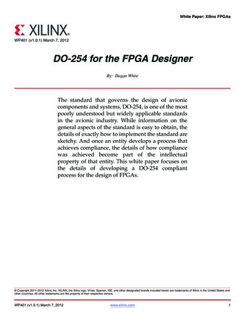
Chapter IIN-AMP BASICSIntroductionBRIDGE SUPPLYVOLTAGEInstrumentation amplifiers (in-amps) are sometimesmisunderstood. Not all amplifiers used in instrumentation applications are instrumentation amplifiers, and byno means are all in-amps used only in instrumentationapplications. In-amps are used in many applications,from motor control to data acquisition to automotive.The intent of this guide is to explain the fundamentalsof what an instrumentation amplifier is, how it operates,and how and where to use it. In addition, several different categories of instrumentation amplifiers areaddressed in this guide.0.01 F1234Figure 1-1 shows a bridge preamp circuit, a typical in-ampapplication.When sensing a signal, the bridge resistor valueschange, unbalancing the bridge and causing a change indifferential voltage across the bridge. The signal outputof the bridge is this differential voltage, which connectsdirectly to the in-amp’s inputs. In addition, a constant dcvoltage is also present on both lines. This dc voltage willnormally be equal or common mode on both input lines. Inits primary function, the in-amp will normally reject thecommon-mode dc voltage, or any other voltage commonto both lines, while amplifying the differential signal voltage,the difference in voltage between the two lines.7AD8221VOUT6–0.01 FUnlike an op amp, for which closed-loop gain is determined by external resistors connected between itsinverting input and its output, an in-amp employs aninternal feedback resistor network that is isolated from itssignal input terminals.With the input signal applied acrossthe two differential inputs, gain is either preset internallyor is user set (via pins) by an internal or external gainresistor, which is also isolated from the signal inputs.0.33 F8 RGIN-AMPS vs. OP AMPS: WHAT ARE THEDIFFERENCES?An instrumentation amplifier is a closed-loop gainblock that has a differential input and an output thatis single-ended with respect to a reference terminal.Most commonly, the impedances of the two inputterminals are balanced and have high values, typically109 , or greater. The input bias currents should alsobe low, typically 1 nA to 50 nA. As with op amps, outputimpedance is very low, nominally only a few milliohms,at low frequencies. VS5–VSREF0.33 FFigure 1-1. AD8221 bridge circuit.In contrast, if a standard op amp amplifier circuit wereused in this application, it would simply amplify both thesignal voltage and any dc, noise, or other common-modevoltages. As a result, the signal would remain buried underthe dc offset and noise. Because of this, even the bestop amps are far less effective in extracting weak signals.Figure 1-2 contrasts the differences between op amp andin-amp input characteristics.Signal Amplification and Common-Mode RejectionAn instrumentation amplifier is a device that amplifiesthe difference between two input signal voltages whilerejecting any signals that are common to both inputs.Thein-amp, therefore, provides the very important functionof extracting small signals from transducers and othersignal sources.Common-mode rejection (CMR), the property ofcanceling out any signals that are common (the samepotential on both inputs), while amplifying any signalsthat are differential (a potential difference between theinputs), is the most important function an instrumentation amplifier provides. Both dc and ac common-moderejection are important in-amp specifications. Any errorsdue to dc common-mode voltage (i.e., dc voltage presentat both inputs) will be reduced 80 dB to 120 dB by anymodern in-amp of decent quality.However, inadequate ac CMR causes a large, timevarying error that often changes greatly with frequencyand, therefore, is difficult to remove at the IA’s output.Fortunately, most modern monolithic IC in-amps provideexcellent ac and dc common-mode rejection.1-1
Common-mode gain (ACM), the ratio of change inoutput voltage to change in common-mode input voltage, is related to common-mode rejection. It is the netgain (or attenuation) from input to output for voltagescommon to both inputs. For example, an in-amp witha common-mode gain of 1/1000 and a 10 V commonmode voltage at its inputs will exhibit a 10 mV outputchange. The differential or normal mode gain (AD) isthe gain between input and output for voltages applieddifferentially (or across) the two inputs. The commonmode rejection ratio (CMRR) is simply the ratio ofthe differential gain, AD, to the common-mode gain.Note that in an ideal in-amp, CMRR will increase inproportion to gain.Common-mode rejection is usually specified for fullrange common-mode voltage (CMV) change at a givenfrequency and a specified imbalance of source impedance(e.g., 1 k source imbalance, at 60 Hz).Mathematically, common-mode rejection can be represented aswhere:AD is the differential gain of the amplifier;VCM is the common-mode voltage present at theamplifier inputs;VOUT is the output voltage present when a common-modeinput signal is applied to the amplifier.The term CMR is a logarithmic expression of thecommon-mode rejection ratio (CMRR).That is, CMR 20 log10 CMRR.To be effective, an in-amp needs to be able to amplifymicrovolt-level signals while rejecting common-modevoltage at its inputs. It is particularly important for thein-amp to be able to reject common-mode signals over thebandwidth of interest. This requires that instrumentation amplif
tion applications are instrumentation amplifiers, and by no means are all in-amps used only in instrumentation applications. In-amps are used in many applications, from motor control to data acquisition to automotive. The intent of this guide is to explain the fundamentals of what an