Transcription
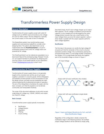
DESIGNERCIRCUITS, LLCDesignNote 001cTransformerless Power Supply DesignGeneral DescriptionTransformerless AC power supplies accept wall-outlet ACvoltage (such as 120VAC) input and produce a low voltageDC (such as 3VDC) output. The low voltage DC is typicallylow current output, on the order of tens of milliamps.This DesignNote explains how transformerless powersupplies work and examines tradeoffs to consider whendesigning them. The options described herein can beimplemented with the ProtoPowerSwitch, a circuit forprototyping products that control AC voltage and/or arepowered by AC voltage.The ProtoPowerSwitch can be ordered pre-populated or as abare board. Beyond the prototyping stage, Designer Circuits,LLC can support transition to production by designing andsourcing custom circuit boards specific to your application.Contact info@designercircuits.com to learn more.Described simply, the AC input voltage charges up an outputfilter capacitor. The AC voltage is rectified to ensure that thecapacitor is only charged and not discharged by the mains.Voltage division ensures that only a small fraction of theinput voltage shows up across the output capacitor. Lastly, aZener diode in parallel with the output capacitor performsbasic voltage regulation.RectificationThe first step in the process is to rectify the high voltage ACsinusoid such that the remainder of the circuit is only everexposed to positive voltage. This is achieved by passing thesinusoid through either (1) a full bridge rectifier composed offour diodes, or (2) a single diode that blocks the negativepart of the sinusoidal voltage, as shown in Figure 1.AC Input VoltageTransformerless AC Power SuppliesTransformerless AC power supply theory is not generallytaught at the university level, yet the use of such powersupplies is prevalent in consumer goods. Online whitepapersand websites provide example circuits and equations to aidthe design process, yet these sources emphasize the mathwithout explaining the fundamental principles of operation.The aim of this DesignNote is familiarize the reader with thebasic concepts, such that the equations can be derived,constructed, and manipulated intuitively.The scope of this document addresses circuits which acceptsingle phase AC voltage (e.g. 120VAC, 240VAC) and outputlow, fixed DC voltage.Output with full-wave rectification (four diodes)Output with half-wave rectification (single diode)Basic ConceptA transformerless power supply typically incorporates: RectificationVoltage DivisionRegulationFilteringInrush LimitingFigure 1 Input and Output Waveforms for Full- and HalfWave Rectification StagesRegardless of the configuration, diodes comprise therectification stage. In the following sections, the rectifiedoutput voltage waveform will be referred to simply as Vin.
DESIGNERCIRCUITS, LLCUsing a High Voltage to Make a Low VoltageA well-known method of generating a low voltage from ahigh voltage is to use a voltage divider circuit, as shown inFigure 2. In textbook examples, the impedances Z1 and Z2 aretypically resistors, and if only negligible current leavesthrough Vout, then the voltage we can expect at Vout is Vin * Z2/ (Z1 Z2).DesignNote 001creverse. This reverse current flow occurs only when thereverse voltage across the Zener diode grows high enoughto match the Zener voltage rating.Note that the Zener diode will actively dissipate power whenreverse current flows through it because there is a voltage(the Zener voltage) across it. This power is P I*V.Using a Zener diode instead of a resistor for Z2 produces abetter power supply which maintains constant outputvoltage despite changes in input voltage or load current.Regardless of whether 1mA or 30mA is flowing through theZener diode, its Zener voltage does not change (much). Thus,Vout also will not change, even if a load connected to Voutdraws current (current that would have otherwise passedthrough the Zener diode).If the small amount of inherent Zener diode voltagevariability is unacceptable, Vout can feed into an LDO orDC/DC power supply, which will provide improved outputregulation.Figure 2 Basic Voltage Divider CircuitUsing resistors for both Z1 and Z2 will generally result in apoor power supply design. Good power supplies support arange of output current from Vout while holding the outputvoltage constant. In a resistor-based design, if there is anyload current then the voltage drop across Z1 will increase andVout will correspondingly decrease, which is undesirable.Another issue is that if Vin were to decrease, then Vout willdecrease by the same proportion. Given that Vin variessignificantly over time (see Figure 1), we know with certaintythat Vout will also vary over time as well, which is againundesirable.To improve the performance of the power supply, we canreplace the Z2 resistor with a Zener diode instead, as shownin Figure 3Constant Power LossThe Zener diode introduces a non-obvious drawbackcommon to all transformerless power supplies: constantpower consumption regardless of load. The currentpassing through Z1 can go one of two places: through theZener diode or through the load connected to Vout. However,the total average current will always match the currentthrough Z1. For a transformerless supply that can source upto 30mA: If the load connected to Vout draws very littlecurrent (or none at all), then all unused current (upto 30mA) flows through Z2 which dissipates powerin the Zener diode.If the load connected to Vout draws most of the30mA, then the power dissipation of the Zener islower while the power dissipation of the load ishigher.Constant average input power input isincurred for a transformerless powersupply regardless of whether or notthe load draws current.Output (Hold-up) CapacitanceFigure 3 Voltage Divider Circuit with ZenerAn ordinary diode will pass current in one direction(indicated by the arrow of the symbol) but will block currentif it tries to flow the other way, preferring instead to allow areverse voltage to build up across it. The Zener diode has theunusual characteristic that above a specified reverse voltage(the Zener voltage) for the device, it will no longer blockcurrent but instead allow current to flow through it inA rectified sinusoidal AC input voltage (as shown in Figure 1)has periods of time where the instantaneous Vin has a smallermagnitude than the DC output (Zener) voltage. To prop upthe DC output voltage during these periods, a capacitor isadded to Vout. This capacitor allows Vout to “ride through” theperiods of small instantaneous AC voltage.
DESIGNERCIRCUITS, LLCDesignNote 001cInput ImpedanceResistive And Capacitive Input ImpedanceZ1 is usually implemented as one of two options. A verysimple low cost Z1 is a resistor; a more efficient option is acapacitor. The size of the Z1 resistor or capacitor and theZener voltage together determine how much total outputcurrent will be available.Blocking Diode PlacementAs mentioned previously, there are both resistive andcapacitive options for the input impedance selection. Thepurpose of the input impedance is to provide a large voltagedrop from Vin to Vout. For resistive input impedance, it shouldcome as no surprise that this large voltage drop generatessubstantial power loss when compared against capacitiveinput impedance.There are two places where blocking diode(s) for rectificationcan be placed: before the Zener diode and after the Zenerdiode.Table 1 provides a comprehensive list of the basictransformerless power supply configurations, along with thetradeoffs encountered by each configuration.In general, placing a blocking diode after the Zener (“postZener”) will prevent the (admittedly small) reverse currentflow from the output capacitor through the Zener. Theoutput capacitor generates reverse current flow through theZener only during portions of the waveform where Vin is lessthan the output capacitor voltage. Inclusion of a Post-Zenerdiode results in a tradeoff that the output voltage willtypically be a diode drop (0.7V) less than the Zener voltage.The basic configurations are constructed from the followingoptions:Full Wave Rectified Circuits:For full-wave rectification to be effective, the rectificationmust be performed before the Zener diode (that is, the fullbridge rectifier must be between the AC source and theZener diode). This is because the Zener diode will onlygenerate the Zener voltage output whenever a reversevoltage is applied to it. Full wave rectification ensures thatVin is positive, which allows the Zener voltage to begenerated. If full wave rectification were added after theZener diode (between the Zener and the output capacitor),then the negative portion of the AC waveform would simplyresult in forward conduction through the Zener, which doesnot generate a useful output voltage. Therefore, for full-waverectification, blocking diodes must always be present beforethe Zener diode (“pre-Zener”). An optional blocking diodemay still be placed after the Zener. However, in full waverectified circuits this is typically not done; the opportunity forthe output capacitor to discharge through the Zener inreverse occurs so infrequently that that the leakage is not aconcern.Half Wave Rectified Circuits:If half wave rectification is used, a single post-Zener blockingdiode may be used with no pre-Zener blocking diode. PostZener blocking diodes provide greater benefit in a half waverectified circuit because (as shown in the waveform of Figure1) at least 50% of the time, Vin sits at 0V, which is less thanthe output voltage, giving plenty of opportunity for capacitorleakage through the Zener. The leakage is even more evidentin low voltage Zener diodes ( 6V typically) because theircurrent-voltage curve tends to be “softer”—that is, the Zenermay start conducting current well before the Zener voltage isreached. In many cases, however, the leakage currents evenwithout a Post-Zener blocking diode is usually low enoughthat it is not a concern. Capacitive or Resistive Input ImpedanceFull Wave or Half Wave RectificationPre-Zener or Post-Zener RectificationNote that full-wave configurations with post-Zenerrectification are entirely excluded from the list because it isnot possible to generate full-wave rectification after theZener has effectively passed only a half-wave rectifiedoutput.The Capacitive Half-Wave Rectified configuration with PreZener Rectification is shown for illustrative purposes only asit does not generate output voltage.Resistive Transformerless AC SupplyThe lowest-cost, physically-smallest component we can usefor input impedance Z1 is a resistor, which we will refer to asR1 or Rin. All load and Zener diode current flows through R1.Large peak voltages (as high as Vin,peak - Vout) will exist acrossR1, so it must be rated to handle high voltage. Thecombination of high voltage and current flow (equal to thetotal load Zener current) results in significant power lost asheat in resistor R1. A resistive transformerless is typicallysized to deliver relatively small amounts of current (a fewmA) so as to limit the heat generated by resistor R1.The power dissipated by resistor R1 for a full-wave rectifier isthe RMS voltage across R1 squared, divided by the resistanceR1. We can approximate the RMS voltage across R1 from theRMS of the input voltage minus the DC output voltage., (, )
DESIGNERCIRCUITS, LLCDesignNote 001cThe equations in the MicrochipApplication Note AN954 (revision A),Transformerless Power Supplies:Resistive and Capacitive and ST! Application Note AN2263 havefundamental errors and the reader isencouraged to use the corrected equationsprovided here, and to verify designsThe above equation should also be used for resistive halfthrough simulation as well.wave rectifiers that do not have a pre-Zener blocking diodTable 1. Transformerless Power Supply Configurations and Tradeoffs-More efficient than resistive-Physically larger and higher material cost than resistive-Provides twice the output current of the half-wave capacitive-DC output ground not tied to AC neutral; cannot drive SCRs/TRIACs directly-More efficient than resistive-Physically larger and higher material cost than resistive-Provides half the output current of the full-wave capacitive-DC output ground tied to AC neutral; SCRs/TRIACs can be driven directly-No reverse current loss from output capacitor through ZenerSimply does not work. Output current for capacitive supply is determined by . The diode blocks capacitorfrom discharging, so 0 andthus 0-Less efficient than capacitive (significant heat generated by Rin)-Physically smaller and lower material cost than capacitive-Provides twice the output current of the half-wave resistive-DC output ground not tied to AC neutral; cannot drive SCRs/TRIACs directly-Rin power loss is twice as much as resistive half-wave pre-Zener-Slight reverse current loss from output capacitor through Zener (can bemitigated with additional blocking diode)-Less efficient than capacitive (significant heat generated by Rin)-Physically smaller and lower material cost than capacitive-Provides half the output current of the full-wave resistive-DC output ground tied to AC neutral; SCR/TRIACs can be driven directly-Output blocking diode drop reduces Vout below Zener voltage-Rin power loss is twice as much as resistive half-wave pre-Zener-No reverse current loss from output capacitor through Zener-Less efficient than capacitive (significant heat generated by Rin)-Physically smaller and lower material cost than capacitive-Provides half the output current of the full-wave resistive-DC output ground tied to AC neutral; SCR/TRIACs can be driven directly-Vout is not reduced by the presence of a blocking diode-Rin power loss is half as much as resistive half-wave post-Zener-Slight reverse current loss from output capacitor through Zener (can bemitigated with additional blocking diode)
DESIGNERCIRCUITS, LLCDesignNote 001cFor a half-wave rectifier with the blocking diode pre-zener,the effective input RMS volta
Note that the Zener diode will actively dissipate power when reverse current flows through it because there is a voltage (the Zener voltage) across it. This power is P I*V. Using a Zener diode instead of a resistor for Z 2 produces a better power supply which maintains constant output voltage despite changes in input voltage or load current.