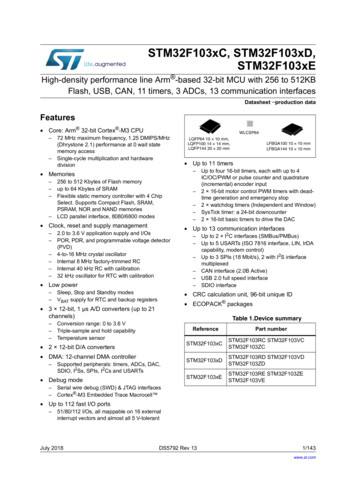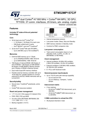
Transcription
Hermes Microvision, Inc. PresentPage : 1Leakage Study of 45nm SRAMDevices with Different LayoutsUsing Advanced e-beamInspection SystemsHong Xiao, Eric Ma, Fei Wang, Yan Zhao, and Jack JauTFUG Meeting: FEoL Integration
List of Topics Page : 2About HMIIntroductionExperiment SetupExperiment ResultsSummaryTFUG Meeting: FEoL Integration
About HMIPage : 3 Founded in June 1998 at silicon valley. Financed by Hermes-Epitek Co. Well established leading EBI systemprovider for wafer and mask defect solution. 38 wafer EBI systems installed worldwide.– Multiple systems in leading foundry fabs.– Multiple systems in leading memory fabs.– Major image sensor manufacturer.– Leading automobile chip manufactures.TFUG Meeting: FEoL Integration
Introduction: EBI BasicsGLV of the pixel isdetermined bynumber of SE fromthat pixel collectedby the detectorTFUG Meeting: FEoL IntegrationPage : 4
Introduction: EBI BasicsPage : 5 Topography contrast (TC)– Physical defects Material contrast (MC)– Physical defects Voltage contrast (VC)– Electrical defects– Mid to high I, low or mid LE for positive mode– High I, High LE for negative modeTFUG Meeting: FEoL Integration
SEM ContrastsPage : 6SETC, MC and VCTC dominateJeong-Geun Park, et. al., Proc. of SPIE, 6299-83 (2006) Local field e-beam MC dominateConducting plugs withthin dielectric capSE SNCTC, MC and VCBVC defectNormally darkSEBSE Nitride cap FloatingplugGroundingplugLuke Lin (PSC) andHong Xiao (HMI), Proc.of ISSM, pp.594, 2007DielectricremainVC dominateTFUG Meeting: FEoL Integration
EBI Inspection ModesPage : 7(SE BSE)/PEE1 LE E2:positive mode1.0LE E2 : negativemodeLE E1:NegativemodeE1Positive Mode, 400eVEE2Positive Mode, 800eVNegative Mode, 2000eVP OpenN OpenTFUG Meeting: FEoL Integration
IntroductionPage : 8 EBI Applications– VC and physical defects Device leakage– NMOS– PMOS– Gate Early detections of device leakage issues– WCMP– NiSiTFUG Meeting: FEoL Integration
Experiment 2 Setup Experiment equipment– eScan Lite Experiment Sample– One 45nm NiSi wafer– One 45nm WCMP wafer– Same mask, same processes until NiSiTFUG Meeting: FEoL IntegrationPage : 9
Sample of Experiment 2SRAM 3SRAM 1TFUG Meeting: FEoL IntegrationPage : 10
Results of Experiment 2Page : 11 PMOS Leakage– DVC of WCMP Negative ModeTM– SRAM 1 & SRAM 3 have different signatures SRAM 1 has “horseshoe” signature SRAM 3 has random signature– SRAM 1 has much more PMOS leakage thanthat of SRAM 3.TFUG Meeting: FEoL Integration
P /N-well Leakage (WCMP DVC)SRAM 152782SRAM 3195Site 1Site 2SRAM 1 site 1SRAM 1 site 2TFUG Meeting: FEoL IntegrationPage : 12SRAM 3
P /N-well Leakage FAPage : 13EDX siteSRAM 1 site 1SRAM 1 site 2SRAM 3ElementWeight%Atomic%OK9.8917.83Si K70.8172.69Ni K19.309.48Totals100.00TFUG Meeting: FEoL Integration
Results of Experiment 2Page : 14 NMOS Leakage– BVC of WCMP positive mode– DVC of WCMP Negative ModeTM– BVC of NiSi positive mode N /P-well leakage has different signaturefrom P /N-well leakage signature inSRAM 1 SRAM 1 and SRAM 3 have different N /Pwell leakage signaturesTFUG Meeting: FEoL Integration
SRAM 1 LeakagePage : 15NiSi: N-leakWCMP: N-leakWCMP: P-leak244305379452782TFUG Meeting: FEoL Integration
SRAM 3 LeakageNiSi: N-leak27857Page : 16WCMP: N-leak22540TFUG Meeting: FEoL IntegrationWCMP: P-leak195
N-Leak/short of SRAM 3Page : 17WCMP Positive ModeWCMP Negative Mode2132022540500eV/50nA3000eV/100nATFUG Meeting: FEoL Integration
N-Leak/short of SRAM 3NiSi: NMOS BVCPage : 18WCMP: NMOS BVCTFUG Meeting: FEoL Integration
More Experiment 2 ResultsPage : 19 Possible contact-to-poly short– Pass gate: WCMP Negative ModeTM DVC– Pass gate: WCMP positive mode Weak BVCGate poly short to N contact plugTFUG Meeting: FEoL Integration
More Experiment 2 Results Gate Leakage: NiSi gate BVCSRAM 1907SRAM 316066TFUG Meeting: FEoL IntegrationPage : 20
More Experiment 2 ResultsPage : 21 NiSi dark defect likely caused by NiSi missingSRAM 12353SRAM 314629TFUG Meeting: FEoL Integration
SRAM 3 NiSi Defect 500011460Gate BVCDark defectNN-leakshortTFUG Meeting: FEoL IntegrationWrongreferencePage : 22
DiscussionPage : 23 Overlap inverter gate and N-well AA Avoid share contact touching STI Over etch can cause PMOS leakageP /N-wellUnit CellP /N-wellcontactShare contactN /P-wellGatesGate contactShuen-chen Lei, et al., Proc. ofSPIE, Vol. 6518, pp. 65184I, (2007)TFUG Meeting: FEoL IntegrationN /P-well contact
Summary of Experiment 2Page : 24 We focused on leak/short in this study:– NiSi EBI captured NMOS and gate leak,– WCMP positive mode captured NMOS leak,– WCMP Negative ModeTM EBI captured PMOS leak,NMOS leak and contact-to-poly short.– Good correlations among positive mode NMOS leak,negative mode NMOS leak and NiSi NMOS leak. SRAM arrays with different layouts havedifferent leakage signatures– SRAM 1 has higher overetch-induced PMOS leakagewhich is sensitive to pattern density. There are different signatures of NMOS andPMOS leakage in the same SRAM array, due todifferent leakage mechanisms.TFUG Meeting: FEoL Integration
Page : 25Comparison of Two ExperimentsExperiment equipmenteScan 310Experiment equipmenteScan LiteExperiment sample45nm WCMP waferExperiment sample45nm WCMP waferNotchRightNotchDownStage/Scan DirectionLS ModeStage/Scan DirectionLS ModeTotal/Inspected Die66/66Total/Inspected Die66/66Landing Energy/B current3000eV / 94 nALanding Energy/B current3000eV / 26.49 nAScan Average1D1L1FScan Average1D1L1FPixel Size40nmPixel Size40nmInspection Time1h0m56sInspection Time44m29sTotal Defect96281Total Defect59420Experiment 1: Sep. 2007Experiment 2: May. 2008TFUG Meeting: FEoL Integration
Page : 26WCMP Negative Mode EBI ResultsWC MP N egative eriment 1 total defects: 9628145NN openleakagePleakageP openExperiment 2 total defect: 59420TFUG Meeting: FEoL Integration
SRAM1 Leakage Summary Experiment 1 Experiment 2 N-leak: 96176 P-leak: 90 N-leak: 3794 P-leak: 52782TFUG Meeting: FEoL IntegrationPage : 27
RecommendationPage : 28 EBI at NiSi to capture N /P-well and gateleakage at the earliest stage. Positive mode EBI at WCMP layer to captureN /P-well leakage, gate leakage and P /N-wellcontact open. Negative ModeTM EBI at WCMP layer to captureP /N-well leakage, N /P-well contact open andpoly-to-contact short. For engineering studies, always review WCMPVC defects with both charging modes.TFUG Meeting: FEoL Integration
AcknowledgementPage : 29 The samples were provided by one of leading ICmanufacturers. Authors deeply appreciate the decision to allowus to published the troubleshooting data andstrictly follow the instruction not to disclose theidentity of sample provider. Many thanks for the valuable supports fromcolleagues in Singapore, US and Taiwan: HeeShing Chua, Wei Fang, Nick Chen, Wayne Chui,Roland Yeh and Joseph Lin. The fine FA jobs were performed by MaterialScience Service in Hsinchu, Taiwan.TFUG Meeting: FEoL Integration
Hermes Microvision, Inc.Thank You!TFUG Meeting: FEoL IntegrationPage : 30
Hermes Microvision, Inc. Present. TFUG Meeting: FEoL Integration List of Topics Page : 2 About HMI Introduction Experiment Setup Experiment Results Summary. TFUG Meeting: FEoL Integration About HMI Page : 3 Founded in June 1998 at silicon valley. Financed by Hermes-Epitek Co.