Transcription
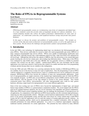
Proceedings of the IEEE, Vol. 86, No. 4, pp. 615-639, April, 1998.The Roles of FPGAs in Reprogrammable SystemsScott HauckDepartment of Electrical and Computer EngineeringNorthwestern UniversityEvanston, IL 60208-3118 USAhauck@ece.nwu.eduAbstractFPGA-based reprogrammable systems are revolutionizing some forms of computation and digital logic.As a logic emulation system they provide orders of magnitude speedup over software simulation. As acustom-computing machine they achieve the highest performance implementation for many types ofapplications. As a multi-mode system they yield significant hardware savings and provide truly generichardware.In this paper we discuss the promise and problems of reprogrammable systems. This includes anoverview of the chip and system architectures of reprogrammable systems, as well as the applications ofthese systems. We also discuss the challenges and opportunities of future reprogrammable systems.1. IntroductionIn the mid 1980s a new technology for implementing digital logic was introduced, the field-programmable gatearray (FPGA). These devices could either be viewed as small, slow mask programmable gate arrays (MPGAs) orlarge, expensive programmable logic devices (PLDs). FPGAs were capable of implementing significantly morelogic than PLDs, especially because they could implement multi-level logic, while most PLDs were optimized fortwo-level logic. Although they did not have the capacity of MPGAs, they also did not have to be custom fabricated,greatly lowering the costs for low-volume parts, and avoiding long fabrication delays. While many of the FPGAswere configured by static RAM cells in the array (SRAM), this was generally viewed as a liability by potentialcustomers who worried over the chip’s volatility. Antifuse-based FPGAs also were developed, and for manyapplications were much more attractive, both because they tended to be smaller and faster due to less programmingoverhead, and also because there was no volatility to the configuration.In the late 1980s and early 1990s there was a growing realization that the volatility of SRAM-based FPGAs wasnot a liability, but was in fact the key to many new types of applications. Since the programming of such an FPGAcould be changed by a completely electrical process, much as a standard processor can be configured to run manyprograms, SRAM-based FPGAs have become the workhorse of many new reprogrammable applications. Someuses of reprogrammability are simple extensions of the standard logic implementation tasks for which the FPGAswere originally designed. An FPGA plus several different configurations stored in ROM could be used for multimode hardware, with the functions on the chip changed in reaction to the current demands. Also, boardsconstructed purely from FPGAs, microcontrollers, and other reprogrammable parts could be truly generichardware, allowing a single board to be reprogrammed to serve many different applications.Some of the most exciting new uses of FPGAs move beyond the implementation of digital logic, and insteadharness large numbers of FPGAs as a general-purpose computation medium. The circuit mapped onto the FPGAsneed not be standard hardware equations, but can even be operations from algorithms and general computations.While these FPGA-based custom-computing machines may not challenge the performance of microprocessors forall applications, for computations of the right form an FPGA-based machine can offer extremely high performance,surpassing any other programmable solution. Although a custom hardware implementation will be able to beat thepower of any generic programmable system, and thus there must always be a faster solution than a multi-FPGAsystem, the fact is that few applications will ever merit the expense of creating application-specific solutions. AnFPGA-based computing machine, which can be reprogrammed like a standard workstation, offers the highestrealizable performance for many different applications. In a sense it is a hardware supercomputer, surpassingtraditional machine architectures for certain applications. This potential has been realized by many different
research machines. The Splash system [Gokhale90] has provided performance on genetic string matching that isalmost 200 times greater than all other supercomputer implementations. The DECPeRLe-1 system [Vuillemin96]has demonstrated world-record performance for many other applications, including RSA cryptography.One of the applications of multi-FPGA systems with the greatest potential is logic emulation. The designers of acustom chip need to verify that the circuit they have designed actually behaves as desired. Software simulation andprototyping have been the traditional solution to this problem. However, as chip designs become more complex,software simulation is only able to test an ever decreasing portion of the chip’s computations, and it is quiteexpensive in time and money to debug by repeated prototype fabrications. The solution is logic emulation, themapping of the circuit under test onto a multi-FPGA system. Since the logic is implemented in the FPGAs in thesystem, the emulation can run at near real-time, yielding test cycles several orders of magnitude faster thansoftware simulation, yet with none of the time delays and inflexibility of prototype fabrications. These benefitshave led many of the advanced microprocessor manufacturers to include logic emulation in their validationprocess.In this paper we discuss the different applications and types of reprogrammable systems. In section 2 we presentan overview of FPGA architectures, as well as FPICs. Then, section 3 details what kinds of opportunities thesedevices provide for new types of systems. We then categorize the types of reprogrammable systems in section 4,including coprocessors and multi-FPGA systems. Section 5 describes in depth the different multi-FPGA systems,highlighting their important features. Finally, sections 6 and 7 conclude with an overview of the status ofreprogrammable systems and how they are likely to evolve. Note that this paper is not meant to be a catalog ofevery existing reprogrammable architecture and application. We instead focus on some of the more importantaspects of these systems in order to give an overview of the field.2. FPGA TechnologyOne of the most common field-programmable elements is programmable logic devices (PLDs). PLDs concentrateprimarily on two-level, sum-of-products implementations of logic functions. They have simple routing structureswith predictable delays. Since they are completely prefabricated, they are ready to use in seconds, avoiding longdelays for chip fabrication. Field-Programmable Gate Arrays (FPGAs) are also completely prefabricated, butinstead of two-level logic they are optimized for multi-level circuits. This allows them to handle much morecomplex circuits on a single chip, but it often sacrifices the predictable delays of PLDs. Note that FPGAs aresometimes considered another form of PLD, often under the heading Complex Programmable Logic Device(CPLD).PolysiliconFieldOxideN diffusionONODielectricFigure 1. Actel’s Programmable Low Impedance Circuit Element (PLICE). As shown at left, anunblown antifuse has an oxide-nitride-oxide (ONO) dielectric preventing current from flowing betweendiffusion and polysilicon. The antifuse can be blown by applying a 16 Volt pulse across the dielectric.This melts the dielectric, allowing a conducting channel to be formed (right). Current is then free to flowbetween the diffusion and the polysilicon [Actel94, Greene93].2
access gatefloating gaten sourcen drainP-Type SiliconFigure 2. Floating gate structure for EPROM/EEPROM. The floating gate is completely isolated. Anunprogrammed transistor, with no charge on the floating gate, operates the same as a normal n-transistor,with the access gate as the transistor’s gate. To program the transistor, a high voltage on the access gateplus a lower voltage on the drain accelerates electrons from the source fast enough to travel across the gateoxide insulator to the floating gate. This negative charge then prevents the access gate from closing thesource-drain connection during normal operation. To erase, EPROM uses UV light to accelerate electronsoff the floating gate, while EEPROM removes electrons by a technique similar to programming, but withthe opposite polarity on the access gate [Altera93, Wakerly94].Just as in PLDs, FPGAs are completely prefabricated, and contain special features for customization. Theseconfiguration points are normally either SRAM cells, EPROM, EEPROM, or antifuses. Antifuses are one-timeprogrammable devices (Figure 1), which when “blown” create a connection, while when “unblown” no current canflow between their terminals (thus, it is an “anti”-fuse, since its behavior is opposite to a standard fuse). Becausethe configuration of an antifuse is permanent, antifuse-based FPGAs are one-time programmable, while SRAMbased FPGAs are reprogrammable, even in the target system. Since SRAMs are volatile, an SRAM-based FPGAmust be reprogrammed every time the system is powered up, usually from a ROM included in the circuit to holdconfiguration files. Note that FPGAs often have on-chip control circuitry to automatically load this configurationdata. EEPROM/EPROM (Figure 2) are devices somewhere between SRAM and antifuse in their features. Theprogramming of an EEPROM/EPROM is retained even when the power is turned off, avoiding the need toreprogram the chip at power-up, while their configuration can be changed electrically. However, the high voltagesrequired to program the device often means that they are not reprogrammed in the target system.SRAM cells are larger than antifuses and EEPROM/EPROM, meaning that SRAM-based FPGAs will have fewerconfiguration points than FPGAs using other programming technologies. However, SRAM-based FPGAs havenumerous advantages. Since they are easily reprogrammable, their configurations can be changed for bug fixes orupgrades. Thus they provide an ideal prototyping medium. Also, these devices can be used in situations wherethey can expect to have numerous different configurations, such as multi-mode systems and reconfigurablecomputing machines. More details on such applications are included later in this paper. Because antifuse-basedFPGAs are only one-time programmable, they are generally not used in reprogrammable systems.EEPROM/EPROM devices could potentially be reprogrammed in system, although in general this feature is notwidely used. Thus, this paper will concentrate solely on SRAM-based FPGAs.QP2QREAD or WRITEP4P6P8DATAP1P3OUTP5P7I1 I2 I3Figure 3. Programming bit for SRAM-based FPGAs (left) [Xilinx94], and a 3-input LUT (right).There are many different types of FPGAs, with many different structures. Instead of discussing all of them here,which would be quite involved, this section will present two representative FPGAs. Details on many others can be3
found elsewhere [Brown92, Rose93, Chan94, Jenkins94, Trimberger94, Oldfield95]. Note that reconfigurablesystems can often employ non-FPGA reconfigurable elements; These will be described in section 5.I/O BlocksI/OI/OBlocksBlocksI/O BlocksFigure 4. The Xilinx 4000 series FPGA structure [Xilinx94]. Logic blocks are surrounded by horizontaland vertical routing channels.In SRAM-based FPGAs memory cells are scattered throughout the FPGA. As shown in Figure 3 left, a pair ofcross-coupled inverters will sustain whatever value is programmed onto them. A single n-transistor gate isprovided for either writing a value or reading a value back out. The ratio of sizes between the transistor and theupper inverter is set to allow values sent through the n-transistor to overpower the inverter. The readback featureis used during debugging to determine the current state of the system. The actual control of the FPGA is handledby the Q and Q outputs. One simple application of an SRAM bit is to have the Q terminal connected to the gateof an n-transistor. If a 1 is assigned to the programming bit, the transistor is closed, and values can pass betweenthe source and drain. If a 0 is assigned, the transistor is opened, and values cannot pass. Thus, this constructoperates similarly to an antifuse, though it requires much more area. One of the most useful SRAM-basedstructures is the lookup table (LUT). By connecting 2N programming bits to a multiplexer (Figure 3 right), any Ninput combinational Boolean function can be implemented. Although it can require a large number ofprogramming bits for large N, LUTs of up to 5 inputs can provide a flexible, powerful function implementationmedium.4
Single-Length LinesDouble-Length F4 C4 G4 YQG1C1KF4 C4 G4 YQG1YCLBF1KC3CLBF1F3XYC1G3C3F3XXQ F2 C2 G2G3XQ F2 C2 G2SwitchMatrixSwitchMatrixSwitchMatrixFigure 5. Details of the Xilinx 4000 series routing structure [Xilinx94]. The CLBs (Configurable LogicBlocks) are surrounded by vertical and horizontal routing channels containing Single-Length Lines,Double-Length Lines, and Longlines. Empty diamonds represent programmable connections betweenperpendicular signal lines (signal lines on opposite sides of the diamonds are always connected).One of the best known FPGAs is the Xilinx Logic Cell Array (LCA) [Trimberger93, Xilinx94]. In this section wewill describe their third generation FPGA, the Xilinx 4000 series. The Xilinx array is an Island-style FPGA[Trimberger94] with logic cells embedded in a general routing structure that permits arbitrary point-to-pointcommunication (Figure 4). The only requirement for good routing in this structure is that the source anddestinations be relatively close together. Details of the routing structure are shown in Figure 5. Each of the inputsof the cell (F1-F4, G1-G4, C1-C4, K) comes from one of a set of tracks adjacent to that cell. The outputs aresimilar (X, XQ, Y, YQ), except they have the choice of both horizontal and vertical tracks. The routing structureis made up of three lengths of lines. Single-length lines travel the height of a single cell, where they then enter aswitch matrix (Figure 6 right). The switch matrix allows this signal to travel out vertically and/or horizontallyfrom the switch matrix. Thus, multiple single-length lines can be cascaded together to travel longer distances.Double-length lines are similar, except that they travel the height of two cells before entering a switch matrix(notice that only half the double-length lines enter a switch matrix, and there is a twist in the middle of the line).Thus, double-length lines are useful for longer-distance routing, traversing two cell heights without the extra delayand the wasted configuration sites of an intermediate switch matrix. Finally, longlines are lines that go half thechip height, and do not enter the switch matrix. In this way, very long-distance routes can be accommodatedefficiently. With this rich sea of routing resources, the Xilinx 4000 series is able to handle fairly arbitrary routingdemands, though mappings emphasizing local communication will still be handled more efficiently.5
C1G4G3G2G1C2C3C4DLUTS/RQECYLUTF4F3F2F1LUTYQDS/RQXQ ECKXFigure 6. Details of the Xilinx CLB (left) and switchbox (top right) [Xilinx94]. The multiplexers, LUTs,and latches in the CLB are configured by SRAM bits. Diamonds in the switchbox represent six individualconnections (bottom right), allowing any permutation of connections among the four signals incident tothe diamond.As shown in Figure 6 left, the Xilinx 4000 series logic cell is made up of three lookup-tables (LUTs), twoprogrammable flip-flops, and multiple programmable multiplexers. The LUTs allow arbitrary combinationalfunctions of its inputs to be created. Thus, the structure shown can perform any function of five inputs (using allthree LUTs, with the F & G inputs identical), any two functions of four inputs (the two 4-input LUTs usedindependently), or some functions of up to nine inputs (using all three LUTs, with the F & G inputs different).SRAM controlled multiplexers then can route these signals out the X and Y outputs, as well as to the two flipflops. The inputs at top (C1-C4) provide enable and set or reset signals to the flip-flops, a direct connection to theflip-flop inputs, and the third input to the 3-input LUT. This structure yields a very powerful method ofimplementing arbitrary, complex digital logic. Note that there are several additional features of the Xilinx FPGAnot shown in these figures, including support for embedded memories and carry chains.While many SRAM-based FPGAs are designed like the Xilinx architecture, with a routing structure optimized forarbitrary, long-distance communications, several other FPGAs concentrate instead on local communication. TheCellular style FPGAs [Trimberger94] feature fast, local communication resources, at the expense of more global,long-distance signals. As shown in Figure 7, the CLi FPGA [Jenkins94] has an array of cells, with a limitednumber of routing resources running horizontally and vertically between the cells. There is one localcommunication bus on each side of the cell. It runs the height of eight cells, at which point it enters a repeater.Express buses are similar to local buses, except that there are no connections between the express buses and thecells. The repeaters allow access to the express buses. These repeaters can be programmed to connect together anyof the two local buses and two express buses connected to it. Thus, limited global communication can beaccomplished on the local and express buses, with the local buses allowing shorter-distance communications andconnections to the cells, while express buses allow longer-distance connections between local buses.6
logic cellrepeaterFigure 7. The CLi6000 routing architecture [Jenkins94]. One 8x8 tile, plus a few surrounding rows andcolumns, is shown. The full array has many of these tiles abutted horizontally and vertically.While the local and global buses allow some of the flexibility of the Xilinx FPGA’s arbitrary routing structure,there are significantly fewer buses in the CLi FPGA than are present in the Xilinx FPGA. The CLi FPGA insteadfeatures a large number of local communication resources. As shown in Figure 8, each cell receives two signalsfrom each of its four neighbors. It then sends the same two outputs (A and B) to all of its neighbors. That is, thecell one to the north will send signals AN and BN, and the cell one to the south will send AS and BS, while bothwill receive the same signals A and B. The input signals become the inputs to the logic cell (Figure 9).Instead of Xilinx’s LUTs, which require many programming bits per cell, the CLi logic block is much simpler. Ithas multiplexers controlled by SRAM bits which select one each of the A and B outputs of the neighboring cells.These are then fed into AND and XOR gates within the cell, as well as into a flip-flop. Although the possiblefunctions are complex, notice that there is a path leading to the B output that produces the NAND of the selected Aand B inputs, and sending it out the B output. This path is enabled by setting the two 2:1 multiplexers to theirconstant input, and setting B’s output multiplexer to the 3rd input from the top. Thus, the cell is functionallycomplete. Also, with the XOR path leading to output A, the cell can efficiently implement a half-adder. The cellcan perform a pure routing function by connecting one of the A inputs to the A output, and one of the B inputs tothe B output, or vice-versa. This routing function is created by setting the two 2:1 multiplexers to their constantinputs, and setting A’s and B’s output multiplexer to either of their top two inputs. There are also provisions forbringing in or sending out a signal on one or more of the neighboring local buses (NS1, NS2, EW1, EW2). Notethat since there is only a single wire connecting the bus terminals, there can only be a single signal sent to or7
received from the local buses. If more than one of the buses is connected to the cell, they will be coupled together.Thus, the cell can take a signal running horizontally on an EW local bus, and send it vertically on a NS local bus,without using up the cell’s logic unit. However, by bringing a signal in from the local buses, the cell canimplement two 3-input functions.AAN EW2 BABNAEAWNS1CELLBAAAWNS2NS1BEBWASA EW1 BSAAN EW2 BCELLBBWASA EW1 BSBNAEAAN EW2 BWASA EW1 BSBAAN EW2 BAAAWNS2NS1BBWASBBNAEACELLNS2BBBNAEABBEA EW1 BSAN EW2 BABBBA EW1 BSBNAEBEBAWNS1CELLBBAAN EW2 BABEBA EW1 BSBFigure 8. Details of the CLi routing architecture [Jenkins94].NS1 NS2 EW1 EW21BNBEBSBW1ANAEASAW10B10AD QFigure 9. The CLi logic cell [Jenkins94].The major differences between the Island style architecture of the Xilinx 4000 series and the Cellular style of theCLi FPGA is in their routing structure and cell granularity. The Xilinx 4000 series is optimized for complex,irregular random logic. It features a powerful routing structure optimized for arbitrary global routing, and large8
logic cells capable of providing arbitrary 4-input and 5-input functions. This provides a very flexible architecture,though one that requires many programming bits per cell (and thus cells that take up a large portion of the chiparea). In contrast, the CLi architecture is optimized for highly local, pipelined circuits such as systolic arrays andbit-serial arithmetic. Thus, it emphasizes local communication at the expense of global routing, and has simplecells. Because of the very simple logic cells there will be many more CLi cells on a chip than will be found in theXilinx FPGA, yielding a greater logic capacity for those circuits that match the FPGA’s structure. Because of therestricted routing, the CLi FPGA is much harder to automatically map to than the Xilinx 4000 series, though thesimplicity of the CLi architecture makes it easier for a human designer to hand-map to the CLi’s structure. Thus,in general, cellular architectures tend to appeal to designers with appropriate circuit structures who are willing tospend the effort to hand-map their circuits to the FPGA, while the Xilinx 4000 series is more appropriate forhandling random-logic tasks and automatically-mapped PPPPPPPPPPPPPPPPPPPPPPPFigure 10. The Aptix FPIC architecture [Aptix93a]. The boxed P indicates an I/O pin.Compared with technologies such as full-custom, standard cells, and MPGAs, FPGAs will in general be slower andless dense due to the configuration points, which take up significant chip area, and add extra capacitance andresistance (and thus delay) to the signal lines. Thus, the programming bits add an unavoidable overhead to thecircuit, which can be reduced by limiting the configurability of the FPGA, but never totally eliminated. Also, sincethe metal layers in an FPGA are prefabricated, while the other technologies custom fabricate the metal layers for agiven circuit, the FPGA will have less optimized routing. This again results in slower and larger circuits.However, even given these downsides, FPGAs have the advantage that they are completely prefabricated. Thismeans that they are ready to use instantly, while mask-programmed technologies can require weeks to becustomized. Also, since there is no custom fabrication involved in an FPGA, the fabrication costs can be amortizedover all the users of the architecture, removing the significant NREs of other technologies. However, per-chipcosts will in general be higher, making the technology better suited for low volume applications. Also, sinceSRAM-based FPGAs are reprogrammable, they are ideal for prototyping, since the chips are reusable after bugfixes or upgrades, where mask-programmed and antifuse versions would have to be discarded.A technology similar to SRAM-based FPGAs is Field-Programmable Interconnect Components (FPIC) [Aptix93a]and Devices (FPID) [I-Cube94] (we will use FPIC from now on to refer to both FPIC & FPID devices). Like anSRAM-based FPGA, an FPIC is a completely prefabricated device with an SRAM-configured routing structure(Figure 10). Unlike an FPGA, an FPIC has no logic capacity. Thus, the only use for an FPIC is as a device toarbitrarily interconnect its I/O pins. While this is not generally useful for production systems, since a fixed9
interconnection pattern can be achieved by the printed circuit board that holds a circuit, it can be quite useful inprototyping and reconfigurable computing (these applications are discussed later in this paper). In each of thesecases, the connections between the chips in the system may need to be reprogrammable, or this connection patternmay change over time. In a reconfigurable computer, many different mappings will be loaded onto the system, andeach of them may desire a different interconnection pattern. In prototyping, the connections between chips mayneed to be changed over time for bug fixes and logic upgrades. In either case, by routing all of the I/O pins of thelogic-bearing chips to FPICs, the interconnection pattern can easily be changed over time. Thus, fixed routingpatterns can be avoided, potentially increasing the performance and capacity of the prototyping or reconfigurablecomputing machine.There is some question about the economic viability of FPICs. The problem is that they must provide someadvantage over an FPGA with the same I/O capacity, since in general an FPGA can perform the same role as theFPIC. One possibility is providing significantly more I/O pins in an FPIC than are available in an FPGA. Thiscan be a major advantage, since it takes many smaller I/O chips to match the communication resources of a singlehigh-I/O chip (i.e., a chip with N I/Os requires three chips with 2/3 the I/Os to match the flexibility). However,because the packaging technology necessary for such high I/O chips is somewhat exotic, high-I/O FPICs can beexpensive. Another possibility is to provide higher performance or smaller chip size with the same I/O capacity.Since there is no logic on the chip, the space and capacitance due to the logic can be removed. However, even withthese possible advantages, FPICs face the significant disadvantage that they are restricted to a limited applicationdomain. Specifically, while FPGAs can be used for prototyping, reconfigurable computing, low volume products,fast time-to-market systems, and multi-mode systems, FPICs are restricted to the interconnection portion ofprototyping and reconfigurable computing solutions. Thus, FPICs may never become commodity parts, greatlyincreasing their unit cost.3. Reprogrammable Logic ApplicationsWith the development of FPGAs there are now opportunities for implementing quite different systems than werepossible with other technologies. In this section we will discuss many of these new opportunities, especially thoseof multi-FPGA systems.When FPGAs were first introduced they were primarily considered to be just another form of gate array. Whilethey had lower speed and capacity, and had a higher unit cost, they did not have the large startup costs and leadtimes necessary for MPGAs. Thus, they could be used for implementing random logic and glue logic in lowvolume systems with non-aggressive speed and capacity demands. If the capacity of a single FPGA was notenough to handle the desired computation, multiple FPGAs could be included on the board, distributing thecomputation among these chips.FPGAs are more than just slow, small gate arrays. The critical feature of (SRAM-based) FPGAs is their in-circuitreprogrammability. Since their programming can be changed quickly, without any rewiring or refabrication, theycan be used in a much more flexible manner than standard gate arrays. One example of this is multi-modehardware. For example, when designing a digital tape recorder with error-correcting codes, one way to implementsuch a system is to have separate code generation and code checking hardware built into the tape machine.However, there is no reason to have both of these functions available simultaneously, since when reading from thetape there is no need to generate new codes, and when writing to the tape the code checking hardware will be idle.Thus, we can have an FPGA in the system, and have two different configurations stored in ROM, one for readingand one for writing. In this way, a single piece of hardware handles multiple computations. There have beenseveral multi-configuration systems built from FPGAs, including the just mentioned tape machine, generic printerand CCD camera interfaces, pivoting monitors with landscape and portrait configurations, as well as others[Xilinx92, Fawcett94, Mayrhofer94, Shand95].While the previous uses of FPGAs still treat these chips purely as methods for implementing digital logic, there areother applications where this is not the case. A system of FPGAs can be seen as a computing substrate withsomewhat different properties than standard microprocessors. The reprogrammability of the FPGAs allows one todownload algorithms onto the FPGAs, and change these algorithms just as general-purpose computers can changeprograms. This computing substrate is different from standard processors, in that it provides a huge amount of10
fine-grain parallelism, since there are many logic blocks on the chips, and the instructions are quite simple, on theorder of a single five bit input, one bit output function. Also, while the instruction-stream of a microprocessor canbe arbitrarily complex, with the function computed by the logic changing on a cycle by cycle basis, theprogramming of an FPGA is in general held constant throughout the execution of the mapping (exceptions to thisinclude techniques of run-time reconfigurability described below). Thus, to achieve a variety of different functionsin a mapping, a microprocessor does this temporally, with different functions executed duri
widely used. Thus, this paper will concentrate solely on SRAM-based FPGAs. READ or WRITE DATA Q Q I1I2 I3 OUT P1 P3 P5 P7 P2 P4 P6 P8 Figure 3. Programming bit for SRAM-based FPGAs (left) [Xilinx94], and a 3-input LUT (right). There are many different types of FPGAs, with many different structures. Instead of discussing all of them here,