Transcription
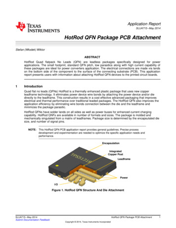
Application ReportSLUA715 – May 2014HotRod QFN Package PCB AttachmentStefan (Włodek) WiktorABSTRACTHotRod Quad flatpack No Leads (QFN) are leadless packages specifically designed for powerapplications. The small footprint, standard QFN pitch, low parasitics along with high current capability ofthese packages are ideal for power converters application. The electrical connections are made via landson the bottom side of the component to the surface of the connecting substrate (PCB). This applicationreport presents users with information about attaching HotRod QFN devices to the printed circuit boards.1IntroductionQuad flat no leads (QFNs) HotRod is a thermally enhanced plastic package that uses new copperleadframe technology. It eliminates power device wire bonds by attaching the power device and/or diedirectly to the leadframe. This construction results in a cost effective advanced packaging that improveselectrical and thermal performance over traditional leaded packages. The HotRod QFN also improves theapplication efficiency by eliminating wire bonds connection between the die and the leadframe andminimizes the package parasitic.HotRod QFNs have solder lands on all sides as well as power buses for enhanced current chargingcapability. HotRod QNFs are available in number of formats and sizes. The package is molded andmechanically singulated from a matrix of leadframes. Package size is determined by the encapsulated diesize, and number of signal pins.NOTE: This HotRod QFN PCB application report provides general guidelines. Precise processdevelopment and experimentation are needed to optimize the specific application needs andperformance.EncapsulationIntegratedCopper PostLeadframePowerI/OFigure 1. HotRod QFN Structure And Die AttachmentSLUA715 – May 2014Submit Documentation FeedbackHotRod QFN Package PCB AttachmentCopyright 2014, Texas Instruments Incorporated1
Manufacturing Considerationwww.ti.comFigure 2. Package Outline2Manufacturing Consideration2.1SMT ProcessFigure 3. Die to Leadframe InterfaceMany factors contribute to a high-yielding assembly process. Table 1 highlights the key elements of SMTprocess.Table 1. SMT EssentialsSMTESSENTIAL2DESCRIPTIONSolder paste qualityUniform viscosity and texture. Free from foreign materials. Solder paste must be used before theexpiration date. Shipment and storage temperature must be maintained at the proper level. Paste mustbe protected from drying out on the solder stencil.PCB qualityHotRod QFN is intended for power application and copper thickness of between 2 oz. and 3 oz. isrecommended for the best electrical performance. The plated solder land area must be clean and flat.The attachment surface must be clean and free of solder-mask residue.Placement accuracyTight tolerances are not required. The QFN package self-aligns as long as the major portion of theleadframe is in contact with the solder paste covering the land areas on the board. Use the alignmentmarks on the PCB are to help verify correct placement of parts.Solder reflow profileThe solder reflow temperature is dependent on the PCB design, PCB thickness and the peak reflowtemperature according to the moisture sensitivity level (MSL) of components and the recommendedprofile of the solder paste being used. A reflow profile must be developed for each PCB type andHotRod QFN packages.Solder volumeSolder volume is important to ensure optimum contact of all intended solder connections.HotRod QFN Package PCB AttachmentSLUA715 – May 2014Submit Documentation FeedbackCopyright 2014, Texas Instruments Incorporated
Stencil Vitalswww.ti.com3Stencil VitalsTI recommends stencil manufacturing by either, laser cut, electro polished or electroform.3.1Solder PasteTI recommends the use of type 3 solder paste when mounting HotRod QFN parts. The use of paste offersthe following advantages: It acts as a flux to aid wetting of the solder to the PCB land The adhesive properties of the paste hold the component in place during reflow Paste contributes to the final volume of solder in the joint, and thus allows this volume to be varied togive optimum joint. Paste selection is normally driven by overall system assembly requirements. In general, the No Cleanflux composition are preferred due to the difficulty in cleaning under the mounted componentsThe HotRod QFN series packages do not require underfill to be utilized.Ti recommends controlled placement pressure in mounting the HotRod packages. Recommended forceshould be controlled to a 5-N maximum for static and a 2.5-N maximum for impact.4Printed Circuit Board (PCB) Design GuidelinesOne of the key components in implementing HotRod QFN package on a substrate is the design of theland pads. The QFN has lead fingers exposed on the bottom side of the package. Electrical, thermal andmechanical connections between the component and motherboard can be made by soldering the partusing screen printed solder paste and reflowing after placement. To ensure consistent solder jointgeometries, it is critical to design the land pattern consistent with the exposed leadframe pattern.4.1Land Pad StyleThere are two basic designs for PCB land pads for the HotRod QFN package the copper defined or non-solder mask defined style (NSMD) and the solder mask defined style (SMD)Either style is acceptable for use with the HotRod QFN package.4.2Land Pad DesignPublication IPC-7351 available from IPC (Association Connecting Electronics Industries ) is one of theindustry standard guidelines for developing PCB pad patterns. Because the HotRod QFN package is anew style, this application report is intended as a guide and should be used with the IPC-7351 publicationin designing an optimum PCB land pattern.SLUA715 – May 2014Submit Documentation FeedbackHotRod QFN Package PCB AttachmentCopyright 2014, Texas Instruments Incorporated3
Printed Circuit Board (PCB) Design Guidelineswww.ti.comFigure 4. PCB Land Pattern4HotRod QFN Package PCB AttachmentSLUA715 – May 2014Submit Documentation FeedbackCopyright 2014, Texas Instruments Incorporated
Printed Circuit Board (PCB) Design Guidelineswww.ti.comAAll linear dimensions are in millimeters.BThis drawing is subject to change without notice. Click here to receive the latest drawing. (SLUSCPublication IPC-7351 from the Association Connecting Electronics Industries (IPC) is recommended for alternatedesignsDThis package is designed to be soldered to a thermal pad on the boards. Refer to SLUA271 and the device-specificdata sheet.ELaser cutting aperture with trapezoidal walls and also rounding corners offer better paste release. Customer shouldcontact their board assembly site for stencil design recommendation. Refer to IPC 7525 the Association ConnectingElectronics Industries (IPC) for stencil design considerations.FCustomers should consult their board fabrication site to obtain metrics that describe the minimum solder mask webtolerance between signal padsFigure 5. HotRod QFN Outline DimensionsSLUA715 – May 2014Submit Documentation FeedbackHotRod QFN Package PCB AttachmentCopyright 2014, Texas Instruments Incorporated5
Layout Guidelines5www.ti.comLayout GuidelinesThe HotRod/QFN application applies mainly to the synchronous, half-bridge power stage and has twoprimary current loops. The input current loop that carries a discontinuous current with high AC content The output current loop that carries continuous current with high DC content.Figure 6. Application Layout ExampleThe input current loop includes the input capacitors, the integrated main switching MOSFET, the inductor,the output capacitor and the ground path back to the input capacitor. It is a good practice to keep this loopas small as possible and place some ceramic capacitors directly between VIN pin and PGND-pin, seeFigure 6. On the PCB layout using HotRod/QFN package the best location for the input bypasscapacitance is on the bottom side of the PCB, directly connected to and underneath the HotRod VINPGNG PCB landing pads.6HotRod QFN Package PCB AttachmentSLUA715 – May 2014Submit Documentation FeedbackCopyright 2014, Texas Instruments Incorporated
Layout Guidelineswww.ti.comTo accomplish it the vias must be placed underneath the device package between the power pads and thesignal pins or on the power pads directly. Additional vias can be placed outside of the package footprintfor improved electrical and thermal conduction to inner layers of the PCB as shown in Figure 7 andFigure 8. The top-side placement for the VIN bypass capacitance is also available with similarperformance to the bottom installation. The signal pins on the VIN-PGND side route through vias to thebottom or inner layer level of PCB to allow for the placement of VIN bypass capacitors.Figure 7. PCB Top LayerSLUA715 – May 2014Submit Documentation FeedbackHotRod QFN Package PCB AttachmentCopyright 2014, Texas Instruments Incorporated7
Layout Guidelineswww.ti.comFigure 8. PCB Bottom LayerThe output current loop includes the SW pin, Integrated SR MOSFET, the inductor, the output capacitorsand the ground return between the output capacitors and the PGND pins. As with the input current loop,maintain the ground return between output capacitor ground and PGND pin as short as possible. On thePCB layout, the best location for the output capacitance is on the top side of the PCB, directly connectedto the output inductor.Maintain the SW node area as small as possible to reduce the parasitic capacitance and minimize theradiated emissions.HotRod/QFN allows for combining the MOSFETs and the control circuitry in a single package. It offers ahigh level of integration, the input and the output loop area can be minimized achieving low parasiticimpedances, higher efficiency, higher power density, higher reliability (bond wires are eliminated), andreduced EMI. Figure 7 and Figure 8 show the example layout.8HotRod QFN Package PCB AttachmentSLUA715 – May 2014Submit Documentation FeedbackCopyright 2014, Texas Instruments Incorporated
Rework Guidelineswww.ti.comFigure 9. TPS54020 PMP9194 with HotRod Package in PlaceA Reference Design for the TPS54020 device is available in the TI Designs section of our website.PMP9194Follow these general guidelines for an efficient PCB layout. Separate the power and signal GND using 0-Ω resistor or a gap. Place it near the device GNDterminal. Use traces as wide as possible on VIN, PGND and SW with some vias to improve thermal aspect ofthe layout.6Rework GuidelinesAfter PCB assembly, the package should be inspected for the assembly defects such as voids, solderballing or other defects underneath the package. The HotRod QFN package offers the external side-filletsolder joint inspection and repair. To rework defects underneath the package on the power bus, the entirepackage must be removed.6.1Component RemovalThe most simple method to remove the HotRod package from the PCB is to use the reflow profile for partremoval similar to the component attachment.Alternatively, the repair station uses the heating source from bottom of the board along with the top sidehot gas nozzle to direct heat at the component to aid in its removal.SLUA715 – May 2014Submit Documentation FeedbackHotRod QFN Package PCB AttachmentCopyright 2014, Texas Instruments Incorporated9
Rework Guidelineswww.ti.comFigure 10. Manual Rework Station for HotRod/QFN Package Devices10HotRod QFN Package PCB AttachmentSLUA715 – May 2014Submit Documentation FeedbackCopyright 2014, Texas Instruments Incorporated
IMPORTANT NOTICE FOR TI DESIGN INFORMATION AND RESOURCESTexas Instruments Incorporated (‘TI”) technical, application or other design advice, services or information, including, but not limited to,reference designs and materials relating to evaluation modules, (collectively, “TI Resources”) are intended to assist designers who aredeveloping applications that incorporate TI products; by downloading, accessing or using any particular TI Resource in any way, you(individually or, if you are acting on behalf of a company, your company) agree to use it solely for this purpose and subject to the terms ofthis Notice.TI’s provision of TI Resources does not expand or otherwise alter TI’s applicable published warranties or warranty disclaimers for TIproducts, and no additional obligations or liabilities arise from TI providing such TI Resources. TI reserves the right to make corrections,enhancements, improvements and other changes to its TI Resources.You understand and agree that you remain responsible for using your independent analysis, evaluation and judgment in designing yourapplications and that you have full and exclusive responsibility to assure the safety of your applications and compliance of your applications(and of all TI products used in or for your applications) with all applicable regulations, laws and other applicable requirements. Yourepresent that, with respect to your applications, you have all the necessary expertise to create and implement safeguards that (1)anticipate dangerous consequences of failures, (2) monitor failures and their consequences, and (3) lessen the likelihood of failures thatmight cause harm and take appropriate actions. You agree that prior to using or distributing any applications that include TI products, youwill thoroughly test such applications and the functionality of such TI products as used in such applications. TI has not conducted anytesting other than that specifically described in the published documentation for a particular TI Resource.You are authorized to use, copy and modify any individual TI Resource only in connection with the development of applications that includethe TI product(s) identified in such TI Resource. NO OTHER LICENSE, EXPRESS OR IMPLIED, BY ESTOPPEL OR OTHERWISE TOANY OTHER TI INTELLECTUAL PROPERTY RIGHT, AND NO LICENSE TO ANY TECHNOLOGY OR INTELLECTUAL PROPERTYRIGHT OF TI OR ANY THIRD PARTY IS GRANTED HEREIN, including but not limited to any patent right, copyright, mask work right, orother intellectual property right relating to any combination, machine, or process in which TI products or services are used. Informationregarding or referencing third-party products or services does not constitute a license to use such products or services, or a warranty orendorsement thereof. Use of TI Resources may require a license from a third party under the patents or other intellectual property of thethird party, or a license from TI under the patents or other intellectual property of TI.TI RESOURCES ARE PROVIDED “AS IS” AND WITH ALL FAULTS. TI DISCLAIMS ALL OTHER WARRANTIES ORREPRESENTATIONS, EXPRESS OR IMPLIED, REGARDING TI RESOURCES OR USE THEREOF, INCLUDING BUT NOT LIMITED TOACCURACY OR COMPLETENESS, TITLE, ANY EPIDEMIC FAILURE WARRANTY AND ANY IMPLIED WARRANTIES OFMERCHANTABILITY, FITNESS FOR A PARTICULAR PURPOSE, AND NON-INFRINGEMENT OF ANY THIRD PARTY INTELLECTUALPROPERTY RIGHTS.TI SHALL NOT BE LIABLE FOR AND SHALL NOT DEFEND OR INDEMNIFY YOU AGAINST ANY CLAIM, INCLUDING BUT NOTLIMITED TO ANY INFRINGEMENT CLAIM THAT RELATES TO OR IS BASED ON ANY COMBINATION OF PRODUCTS EVEN IFDESCRIBED IN TI RESOURCES OR OTHERWISE. IN NO EVENT SHALL TI BE LIABLE FOR ANY ACTUAL, DIRECT, SPECIAL,COLLATERAL, INDIRECT, PUNITIVE, INCIDENTAL, CONSEQUENTIAL OR EXEMPLARY DAMAGES IN CONNECTION WITH ORARISING OUT OF TI RESOURCES OR USE THEREOF, AND REGARDLESS OF WHETHER TI HAS BEEN ADVISED OF THEPOSSIBILITY OF SUCH DAMAGES.You agree to fully indemnify TI and its representatives against any damages, costs, losses, and/or liabilities arising out of your noncompliance with the terms and provisions of this Notice.This Notice applies to TI Resources. Additional terms apply to the use and purchase of certain types of materials, TI products and services.These include; without limitation, TI’s standard terms for semiconductor products http://www.ti.com/sc/docs/stdterms.htm), evaluationmodules, and samples (http://www.ti.com/sc/docs/sampterms.htm).Mailing Address: Texas Instruments, Post Office Box 655303, Dallas, Texas 75265Copyright 2017, Texas Instruments Incorporated
Publication IPC-7351 available from IPC (Association Connecting Electronics Industries ) is one of the industry standard guidelines for developing PCB pad patterns. Because the HotRod QFN package is a new style, this application report is intended as a guide and should be used with the IPC-7351 publication in designing an optimum PCB land pattern.