Transcription
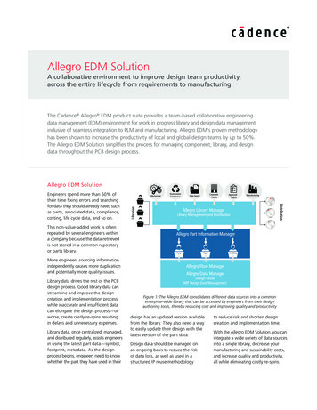
DATASHEETALLEGRO PCB ROUTERTODAY’S LEADING SOLUTION FOR INTERCONNECT ROUTINGThe Cadence Allegro PCB Router — an integral part of the Allegro systeminterconnect design platform — is the market’s leading solution for automatic andinteractive interconnect routing. Designed to handle routing challenges fromsimple designs to high-density PCBs requiring complex, high-speed design rules,the Allegro PCB Router uses powerful shape-based algorithms to make the mostefficient use of the routing area. The result is increased productivity and shorterdesign cycles.IC packagedesignPCB designPackagedesign-in kitSilicondesign-in tual systeminterconnectmodelOn-target, on-timesystem interconnectCorrelateExploreSpecifyI/O bufferIPI/O bufferdesignIC designThe Allegro system interconnect design platformTHE ALLEGRO PCB ROUTERThe Allegro PCB Router is an integralpart of the Cadence Allegro PCBEditor, IC packaging, and Allegro PCBSI 610 product solutions and isintegrated with most of the popularPCB CAD systems. The comprehensivecapabilities of Allegro PCB Routerinclude controllable, true 45-degreerouting that can be used on all nets ororthogonal corner mitering.THE ALLEGRO SYSTEMINTERCONNECT DESIGNPLATFORMThe Cadence Allegro systeminterconnect design platformenables collaborative design of highperformance interconnect across IC,package, and PCB domains. Theplatform’s unique co-designmethodology optimizes systeminterconnect — between I/O buffersand across ICs, packages, and PCBs —to eliminate hardware re-spins,decrease costs, and reduce designcycles. The Allegro constraint-drivenflow offers advanced capabilities fordesign capture, signal integrity, andphysical implementation. With silicondesign-in kits, IC companies shortennew device adoption time and systemscompanies accelerate PCB design cyclesfor rapid time to profit. Supported bythe Cadence Encounter and Virtuoso platforms, the Allegro co-designmethodology ensures effective designchain collaboration.
FEATURES Available on Windows, UNIX, andLinux operating systems with licensingthat floats between platforms High-speed rules/constraint supportfor delay, crosstalk, impedance control,differential pair, and net scheduling —including virtual pinsWhen faced with a dense, highlyconstrained multilayer design, only oneautorouter consistently delivers — theAllegro PCB Router Real-time routing to net scheduling,delay, crosstalk, impedance, anddifferential pair rules Auto net shielding with autovia stitching True 45-degree or orthogonal routing Full Microvia structure support Layer Set routing Recursive mitering engine for handrouted–looking results Interactive routing and componentfloorplanning capabilities Automatic component floorplanningMore than just an autorouter, the AllegroPCB Router offers a complete interconnectenvironment with interactive and automaticcomponent floorplanning, as well asshape-based, 45-degree, interactive, andautomatic routing Seamless integration with Allegro PCBEditor, Allegro Package Designer 610,and Allegro PCB SI 610 Interfaces available for Mentor BoardStation and Mentor PowerPCBHIGH-SPEED, RULES-DRIVENROUTINGAllegro PCB Router high-speedfeatures provide the capabilities tohandle net scheduling, timing,crosstalk, layer set routing, and specialgeometry requirements demanded bytoday’s high-speed circuits.NET TOPOLOGYNet topology scheduling defines therouting order of the pins on a net andeven insert intermediate routing pointsknown as T-points. This allows designersto apply constraints to each segmentof the schedule for precise interconnectcontrol, even when a net contains adiscrete device such as a terminationresistor. With every topologyconstrained net, you can control thelength of your conductors using delayor length specifications. You can alsodefine the minimum or maximumconductor delay or length to ensure aparticular signal arrives at its destinationwithin a specified time period.2CROSSTALKCrosstalk is limited by geometric orparallelism rules. You can define theacceptable gap and length parameters,and the Allegro PCB Routerautomatically separates the parallellines after a specified distance. Youcan also create a gap versus lengthtable to more accurately modelcrosstalk. Crosstalk is reduced byevaluating the geometric or physicallayout of conductors and the electricalproperties of signals carried by theconductors. Noise associated withconductors both on the same layerand adjacent layers is considered.Cumulative noise crosstalk is controlledby coupled noise rules thatincorporate the design’s electricalproperties. Users can define themaximum cumulative crosstalk noisein millivolts allowed by each class ornet. PCB Router dynamically computesthe maximum cumulative crosstalknoise during routing by adding allparallel and tandem conductors.LAYER SETLayer Set routing defines routing layer“sets” and uses them to controlrouting. During routing of impedancecontrolled trace(s) or buses, a layerchange may be necessary in order tocomplete routing. These changes inlayers, if not controlled, can causechanges in impedance based on wherethe new layer is located in the PCBstack up. To eliminate this problem,the desired target layer(s) will havethe same characteristic impedance asthe source layer. The Layer Set featureallows the definition of a number oflayer sets on which the net or bus isallowed to be routed. This is usuallyrelated to the similar impedancevalues of those particular layers in theset. Layers not included in the set willnot be available for routing.DIFFERENTIAL PAIRS, SHIELDED NETS,AND AREA RULESPCB Router also has the flexibility tohandle the special geometry requirementsof high-performance designs. Fordifferential pair routing, users definethe gap between the two conductorsand the autorouter takes care of therest. PCB Router intelligently handles
Shielded signals get auto-generated shieldswith vias inserted at user-defined intervals,tying the shield to the ground layerThe Allegro PCB Router automaticallyhandles differential pairs, maintainingspacing and parallelism rulesrouting around or through vias andautomatically conforms to any definedminimum length criteria. Automatic netshielding is used to reduce noise onnoise-sensitive nets. Separate designrules may be applied to differentregions of the design. For example, youcan specify tight clearance rules in theconnector area of your design and lessstringent rules elsewhere.conserves design space because onlythe selected signals use larger vias.Additionally, you can improve signalimpedance matching by assigningdifferent width and clearance rules todifferent layers.With signal margins shrinking rapidly,the use of net shielding is becomingcommonplace on most high-speeddesigns. In order for net shielding toperform correctly, a shield needs to beconnected to the ground plane atregular intervals so that any straynoise can be effectively absorbed. PCBRouter not only auto-generates theshield around specified nets, but italso ties the shield route to the chosenground plane by automaticallyinserting vias at specified distances.ADVANCED PHYSICAL RULESThe advanced rule set feature withinPCB Router enables electricalparameter control, crosstalk reporting,and conductor-length rule violations —requirements demanded by today’slarge designs. Electrical parametercontrols include the flexibility toassign specific rules to each element inyour design. Users define the rulesrequired to meet the electrical classcharacteristics unique to each layer, viatype, conductor width, or set ofconnections. Using this feature, alarger via can be used to support theincreased current capacity required bypower and ground connections. ThisOuter layers generally have higherimpedance and are assigned largerconductor widths. Inner layers generallyhave lower impedance and areassigned narrower widths to match theimpedance of the outer layers.Impedance matching can also beimproved by controlling routed nets oncertain layers or layer pairs. Reportsinclude coupled noise by using thegeometric or physical layout ofconductors and electrical properties ofsignals. Noise associated with signals onthe same layer and on adjacent layers isconsidered. Possible timing problemsare reported by showing minimum andmaximum wire length violations. All ofthis information is reported in a fileand displayed graphically.MICROVIA RULESWith today’s dense multilayer designs,many companies are considering thebenefits of multilayer build-uptechnologies that employ newmanufacturing techniques to greatlyreduce board size and layer count andto increase signal performance. One ofthe major requirements for these newbuild-up technologies is the support ofcomplex via structures. The AllegroPCB Router Microvia functionality wasdeveloped with Matsushita for thesupport of Matsushita’s industryleading ALIVH technology. This optionincludes support for plural vias (i.e., acluster or array of vias), which allowsfor greater current capacity in widetraces. Stacked vias permit blind andburied vias to be stacked in the sameX-Y location on different layers of theboard. Enhanced via fanout allowsblind and buried vias under SMD pads.When the Microvia feature is selected,the fanout feature allows stacked viasunder SMD pads even when there arepads directly opposite each other onboth sides of the board.ADVANCED SUBSTRATE RULESPCB Router provides capabilitiesto handle blind or buried vias,wirebonding, and vias under surfacemounted pads — requirementsdemanded by today’s ceramic PCBand IC packages. Blind and buried viacontrols automatically use blind orburied vias, when required, totransition between layers. You controlthe clearance between vias ondifferent layers as well as the clearancebetween adjacent vias on the samelayer. You can place a via under anSMD pad at the origin or at the gridpoint nearest the origin. You can alsocontrol whether vias placed underSMD pads fit entirely within theboundary of the pad. If the via shapeon the pad layer extends beyond apad’s boundary, the via is not placed.Wirebond support automaticallyhandles devices that requirewirebonding. Bond sites are placedand automatically routed with discretewires from each site to the pads of achip mounted on the PCB. You definethe type of bond site and the maximumacceptable distance between thecomponent pad and the bond site.DESIGN FOR MANUFACTURINGThe PCB Router‘s design formanufacturing capability significantlyimproves manufacturing yields with aspread command that automaticallyincreases conductor clearances on aspace-available basis. It also miterscorners and adds test pointsautomatically after autorouting.3
Automatic conductor spreading is usedto improve manufacturability byrepositioning conductors to createextra space between conductors andpins, conductors and SMD pads, andadjacent conductor segments. Usershave the flexibility to define a rangeof spacing values or to use the defaultvalues. Miter corners automaticallyreplace 90-degree corners with achamfer by using either the default ora user-specified setback value. You canmiter corners throughout the entiredesign or on specific layers and specifya single value or a range of setbackvalues. The design for manufacturingcapability automatically uses theoptimal setback within the range,starting from the largest to thesmallest value.TEST POINT INSERTIONTest point insertion automatically addstestable vias or pads as test points.Testable vias can be probed on thefront, back, or both sides of the PCB,thereby supporting both single side andclamshell testers. You have theflexibility to select the test pointinsertion methodology that conformsto your manufacturing requirements.Test points can be “fixed” to avoidcostly test fixture modifications. Testpoint constraints include test probesurfaces, via sizes, via grids, andminimum center-to-center distance.useful for placing connectors andcomponents with fixed locations.Density analysis graphically displayscircuit congestion by overlaying thePCB with a color map showing highlycongested areas in relation to lightlycongested areas. This helps youdetermine where placementadjustments might be made to relievecongestion and improve routing.ALLEGRO PCB ROUTERAUTOPLACEMENTAllegro PCB Router autoplacement is ashape-based automatic componentplacement program that supportsboards with 256 routing layers andunlimited component pins. It allowsplacement of components without theneed for grid definitions or lengthysetup for different size components.Autoplacement allows you to placesome components interactively whileautomatically placing others. Roomscan be defined for split power, heightconstraints, power dissipation, or forseparation of analog, CPU, memory,TTL, and ECL circuitry. It can positioncomponents on both sides of the PCBsimultaneously with front-to-backalignment of SMDs. To address theneeds of pick-and-place machines,spacing rules can be defined by layer,component type, or specific component.ROUTE EDITORALLEGRO PCB ROUTERPLACEMENT EDITORThe Allegro PCB Router PlacementEditor allows you to place componentsquickly while simultaneously evaluatingspace, logic flow, and congestionbefore beginning to route your PCB.Move mode allows components to beflipped, rotated, aligned, pushed, andmoved either as individual componentsor as a group.Guided-place mode selects thecomponent with the highestconnectivity and computes an optimalplacement location that does notviolate design rules or constraints.Users have the option of accepting orrejecting the location. You can alsoplace components by directly enteringtheir X-Y locations. This is particularly4The fully integrated Route Editorrevolutionizes the editing processwith its advanced routing andediting capabilities.PLOWING, SHOVING, AND GHOSTINGAs new conductors are routed, theplowing feature automatically pushesexisting conductors aside and routesaround pins. Using the shovingfeature, you can move conductorsegments or vias against existingtraces and push ahead — over otherpins and vias if necessary. The ghostingfeature makes the evaluation of“what if” scenarios easy. As aconductor segment or via is movedunder cursor control, the surroundingconductor is shoved and displayeddynamically. You evaluate the adjustedrouting before accepting a finalThe comprehensive set of shape-basedfloorplanning tools in Allegro PCB Routerincludes interactive and automaticcapabilitiesconfiguration. Additionally, a multilevelundo feature allows you to revert toprevious routing configurations.ADVANCED EDITING FEATURESOn dense, multilayer boards, legal viasites can be difficult to find. The RouteEditor lets you position vias by simplyclicking twice at a chosen location. Ifpossible, the chosen site is used byshoving conductors aside on layers asneeded. Otherwise, Route Editordisplays a design rule violation andshows the legal via sites nearby. Copyroute simplifies bus construction byletting you copy an existing route tocomplete unrouted bus connections.The new route uses the same topologywith length automatically adjusted.Route Editor also lets you use thecornering option that works bestfor your design requirements. Useorthogonal, 45-degree, or all-anglerouting — Route Editor willautomatically snap corners to yourpreference. The critic functionremoves extra bend points createdduring the editing process. Select thearea of interest, or the entire board,and critic simplifies routing toimprove manufacturability.LENGTH RULES AND TIMINGCONSTRAINTSWith the high-performance rules inRoute Editor, you can easily route netsto satisfy timing constraints throughthe dynamic application of minimumand maximum length rules. Twoinnovative graphical techniques areprovided to help you route nets withtiming constraints. First, there is adisplay that details length information
Memory bus routing (SMD orthrough-hole) Online design rule checking Multipass recursive miter Online meter displays length tolerance Via rules by net or net class Global violation indicator Wire and clearance rules by layer Dynamically calculates and displaysavailable slack Net/net-class rules by layer Layer set routing Color feedback on all indicatorsand meter Automatic wire spreading Multiple net (bus) routing Automatic test point generation Automatic single net autorouting Soft and hard fencesDynamic push and shove capabilities makeinteractive editing easy on even the mostadvanced designs Blind, buried, and micro vias Vias under SMD pads Automatic wirebonding Automatic gate and pin swappingduring routing Parallelism controlUsers have control over trombone settingsto manage timing-constrained nets withminimum timing constraints Accumulative noise control Maximum/minimum/matched delayand length control User-defined elongation methodologiesthrough a color-coded meter that isupdated as you route. This showswhether your route is satisfyingminimum and maximum lengthconstraints. The meter display iscontrolled by adding the distancerouted to the remaining Manhattanlength to the target. Thisinstantaneous feedback keeps you ontrack and shows you the amount oflength you have left as you route.Second, a graphical display alsoprovides a more global view ofwhether you are meeting timingconstraints. A green polygon displaysaround the current cursor location andthe target pin if you are within amaximum defined length. The polygondoes not display if the maximumlength will be exceeded. A redpolygon displays when minimumlength is violated.ALLEGRO PCB ROUTERFEATURES Routing of up to 256 signal layers True shape-based routing or gridbased autorouting Automatic routing clean-up Automatic differential pair routing Rules/clearance by area Net shielding Virtual pins for topology controlPLACEMENT EDITOR FEATURES Online design rule checking Floorplanning Guided placement mode Flip, rotate, align, push, and moveindividual components or groups ofcomponents Placement density analysis Direct X-Y location componentplacementAUTOPLACEMENT FEATURES Automatic, double-sidedcomponent placementOPERATING SYSTEMSUPPORT Red Hat Linux 7.3, 8.0 Windows 2000 with Service Pack 2,XP Professional Sun Solaris 7, 8, 9 HP-UX 11.0, 11.11i IBM AIX 5.1CADENCE SERVICESAND SUPPORT Cadence application engineers cananswer your technical questions bytelephone, email, or Internet — theycan also provide technical assistanceand custom training Cadence certified instructors teachover 70 courses and bring their realworld experience into the classroom Over 25 Internet Learning Series (iLS)online courses allow you the flexibilityof training at your own computer viathe Internet SourceLink online customer supportgives you answers to your technicalquestions — 24 hours a day, 7 days aweek — including the latest inquarterly software rollups, productchange release information, technicaldocumentation, solutions, softwareupdates, and more Rules by layer, component, and/orcomponent type Automatic gate and pin swapping Auto-clusteringROUTE EDITOR FEATURES SMD fanout to vias Plowing, shoving, and ghosting 45-degree ECO routing Interactive via search5
Allegro PCB Router feature summary for Allegro PCB design 200 & 600 seriesPCB Design 200 series200 series optionsPCB Design 600 seriesALLEGRO PCB ROUTER FEATURES6 signal layer limitx256 signal layer limitxRouter Auto/InteractivexShape-based or gridded autoroutingxxSMD fanout to viasxxTrace width by net and net classesxx45-degree ECO routingxxMemory pattern routing (SMD or through-hole)xxInteractive via searchxxInteractive routing with shoving and plowingxxInteractive floorplanningxxAutoplacementOnline design rule checkingxFlip, rotate, align, push, and move componentsxPlacement density analysisxAllegro PCB Router ADV 6U or 256UxxRouter performancexLayer set rules and routing supportRouter performancexSignals on specific layersRouter PerformancexWidth and clearance rules by layerRouter PerformancexVia rules by net and/or net classRouter PerformancexNet and/or net class rules by layerRouter PerformancexCrosstalk violation reportRouter PerformancexTrace length violation reportRouter PerformancexBlind and buried via supportRouter PerformancexVia under SMD pad checkingRouter PerformancexAutomatic wirebondingRouter PerformancexPlural viasRouter PerformancexStacked viasRouter PerformancexEnhanced via fanoutRouter PerformancexAllegro PCB Router DFM 6U or 256URouter PerformancexAutomatic trace spreadingRouter PerformancexAutomatic via reductionRouter PerformancexAutomatic miter 90 to 45Router PerformancexAutomatic test point generationRouter PerformancexTest point specific clearance rulesRouter PerformancexPCB PerformancexAllegro PCB Router HP 6U or 256UMinimum, maximum, and matched length rulesPCB PerformancexCrosstalk controls on same and adjacent layersPCB PerformancexVirtual pins that can be moved during autoroutingPCB PerformancexParallelism controlled by length and gapPCB PerformancexDifferential pair routingPCB PerformancexAutomatic net shieldingPCB PerformancexDesign rules by areaPCB PerformancexOnline display of length tolerancePCB PerformancexGlobal violation indicatorPCB PerformancexDynamic display of available lengthPCB PerformancexAutomatic single-net routingPCB PerformancexMultiple net/bus routingPCB PerformancexFOR MORE INFORMATIONContact Cadence sales at 1.800.746.6223or visit www.cadence.com foradditional information. To locate aCadence sales office or value-addedreseller (VAR) in your area, visitwww.cadence.com/contact us. 2004 Cadence Design Systems, Inc. All rights reserved.Cadence, the Cadence logo, Allegro, SourceLink, andVirtuoso are registered trademarks, and Encounter is atrademark of Cadence Design Systems, Inc. All others areproperties of their respective holders.4433C 03/04
THE ALLEGRO PCB ROUTER The Allegro PCB Router is an integral part of the Cadence Allegro PCB Editor, IC packaging, and Allegro PCB SI 610 product solutions and is integrated with most of the popular PCB CAD systems. The comprehensive capabilities of Allegro PCB Router include controllable, true 45-degree routing that can be used on all nets or