Transcription
CMPE 310Layout Editor TutorialJordan Bisasky(This tutorial is a continuation of the Capture CIS Tutorial)Allegro PCB DesignAllegro PCB Design is a circuit board layout tool that accepts a layout-compatiblecircuit netlist (ex. from Capture CIS) and generates output layout files that aresuitable for PCB fabrication. This tutorial is the second part of the PCB projecttutorial. Before starting with PCB Design, you must have a completed schematicwith no errors. The beginning of this tutorial runs through how to create a netlistfrom your schematic. Simple steps in producing PCB layout involve importing thenetlist, placing components, routing and generating output files and reports.Capture CIS Tutorial (Continued)Inserting FootprintsFor every part used in the schematic in Design Entry CIS, there must be anaccompanying footprint. The footprints are provided in a zipped folder on the CMPE310 homepage. The footprints should be in a folder in the same directory as theschematic DSN file. There is also a PCB Footprints PDF with the footprint namescorresponding to the parts. For each part, left click and then right click on the part.Select Edit Properties. Under PCB Footprint, insert the footprint name from the PDFand then hit Apply to save.Figure 1: Inserting footprints from Design Entry CIS
CMPE 310Layout Editor TutorialJordan BisaskyCreating the NetlistThe next step is to generate the netlist from the schematic created in Design EntryCIS and then import the netlist to the PCB Editor. We are generating the netlist usingthe command line in Windows XP.First, go to the folder containing your schematic. Create a folder titled “Allegro”.Additionally, verify that your footprints are in a folder titled “Footprint”.Open the command prompt: Start - All Programs - Accessories - Command PromptType “S:” into the command prompt to move to the S drive.Figure 2: Change directory to “S:\” driveMove to the folder containing your schematic: i.e. “cd 310/finalproj/”Now at your project’s directory, type the following command (one line):C:\Cadence\SPB 16.01\tools\capture\pstswp -pst -d "(name of schematic).DSN" -n"allegro" -c "C:\Cadence\SPB 16.01\tools\capture\allegro.cfg"
CMPE 310Layout Editor TutorialJordan BisaskyFigure 3: Running netlistAllegro PCB EditorCreating a boardOpen PCB Editor: Start - All Programs - Cadence SPB 16.01 - PCB Editor- Allegro PCB Design XLCreate a new board by going to File - NewBrowse to the S Drive directory of choice (preferably the same location as yourschematic), insert a Drawing Name and set the Drawing Type to Board.Figure 4: Creating a new boardImporting the NetlistBefore importing the netlist, you must set the directory path to your footprint folder.Setup - User Preferences - Categories: Design Paths - psmpath ( )Add the directory path to your footprint folder. Then click OK to confirm.
CMPE 310Layout Editor TutorialJordan BisaskyFigure 5: Changing footprint pathTo import the schematics from Design Entry CIS:File - Import - LogicFor Import Design Type, set to Design entry CIS (Capture). Place changedcomponent to Always. Leave everything else unchecked. For Import Directory, set tothe allegro folder (i.e. S:/CMPE310/finalproj/allegro).
CMPE 310Layout Editor TutorialJordan BisaskyFigure 6: Import Logic—“Import directory” is the allegro folder foundwithin the project directoryClick Import Cadence. If no output file opens then your netlist was successfullyimported with no errors or warnings. If there are errors, correct your schematic inDesign Entry CIS and re-netlist/import logic until no errors occur.
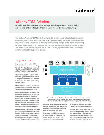
CMPE 310Layout Editor TutorialJordan BisaskySetting up the Board LayersFor the project, we are using a four layer board. The default is two layers so tochange the number, go to Setup - Cross-Section. Right click between the Topand Bottom layers to add four layers. Follow Figure 7 to add the GND and Powerlayers and appropriately set the Type to Dialectric or Plane. The Layout CrossSection should match the figure.Figure 7: Setting the number of layers to fourAllegro PCB Editor settings must be changed to support the board size needed forthe project. To increase the available board size, go to Setup - DesignParameters which opens the Design Parameters Editor. Select the Design tab andchange the Extents to the following: Left X: -500 Lower Y: -500 Width: 15000 Height 15000
CMPE 310Layout Editor TutorialJordan BisaskyThe units are in Mils where 1000 Mils 1 inch. All of the other settings shouldmatch those in Figure 8.Figure 8: Adjusting the Design Parameters Editor to support the requiredboard size
CMPE 310Layout Editor TutorialJordan BisaskyCreating the Board OutlineTo create the board outline: Setup - Outlines - Board OutlineUnder Command Operations, select Create and under Create Options, set to PlaceRectangle.Set the Board Edge Clearance to 100.0 MIL. Set Wdt and Hht both to 12000 MIL (12inches).Do not click OK.Figure 9: Creating the Board OutlinePlace board outline in the lower left hand corner of the window by left clicking.Again, do not click on OK.
CMPE 310Layout Editor TutorialJordan BisaskyFigure 10: Placing the board outlineStill do not click OK, but place the first rectangle in the window by going to Shape- Rectangular. A purple rectangle should appear within the board outline.Go to Options (on the upper right hand corner of the window), select the ActiveClass as Route Keepin and set the Subclass as All. The rectangle color shouldchange from purple to a tannish red.Figure 11: Changing the rectangle classNow create another rectangle overlapping the previous rectangle by again going toShape - Rectangular. Click in the top left corner of the tannish red rectangle andthen click on the lower right corner of the tannish red rectangle. Then right click andselect Done to place the new rectangle.The two rectangles now overlap each other.
CMPE 310Layout Editor TutorialFigure 12: Adding the second rectangleJordan Bisasky
CMPE 310Layout Editor TutorialJordan BisaskyPlacing PartsTo place the parts from the schematic, go to Place - Manually. The parts will bein the Placement menu listed by their part names (i.e. U1, U2, R1, etc). Checkingthe box of one of the parts will allow you to place that part onto the board. Do thisfor all of the parts. When completed, click on OK.Figure 13: Placing parts – Placing the 8086
CMPE 310Layout Editor TutorialJordan BisaskyRoutingFirst, set the width of the wires: Setup - Constraints - Constraint ManagerSelect the Physical tab, select Physical Constraint Set, and then All Layers. UnderType PCS with Objects DEFAULT, set the width under column Line Width Min to 20.0and set the width under Neck Min Width to 20.0.Figure 14: Changing the wire widthsTo route the connections, go to Route - Route Automatic. Leave the settings tothe default and select Route. In the final project, this step can take upwards of 30minutes.Figure 15: Auto routing the parts
CMPE 310Layout Editor TutorialJordan BisaskyDynamic Shapes (for Ground/Power Planes)In the PCB Editor, goto menu Shape - Global Dynamic Params.Global Dynamic Shape Parameters window appears. Select the following:Tab Shape Fill Dynamic Fill: SmoothTab Void controls Artwork format: Gerber RS274XMinimum aperature for gap width: 4.0Suppress shapes less than: 25 milsCreate pin voids: IndividuallyAcute angle trim control: RoundTab Clearances: left as isTab Thermal relief connects: left as isClick [OK]Create Ground/Power Planes:1. In PCB editor, goto menu Shape - Rectangular. On right-hand side ofwindow, mouse-over/select the Options tab. If it is not there, goto MenuView - Window Options. (You may want to click the pin to keep it fromauto-minimizing).For points 2 to 4 refer to figure 16.2. Set the Active Class and Subclass to Etch and then the desired layer GND.3. Set the 'Shape Fill' to Type: Dynamic copper.4. Now, choose to 'Assign a net name' to the rectangle by clicking the ellipsesbutton [.] under Assign net name. Simply select a net name (GND) from thepop-up and click [ok].5. Now draw a shape. It will automatically keep clearances from shape it shouldnot touch as well as produce connections to vias on the same net, where itoverlays them, by making short wires to produces the "thermal" connections.
CMPE 310Layout Editor TutorialJordan BisaskyRepeat steps 1 to 5 for Power plane, selecting net name Vcc.Figure 16: Dynamic Shapes Options TabNOTE: If the dynamic updating ever stops or needs forced updating, goto menuShape Global Dynamic Params., tab Shape fill, and click Update to Smooth.After adding both power & ground planes, check the visibility tab to check theconnections on the different layers. Refer to figure 17.Figure 17: Visibility under Options Tab
CMPE 310Layout Editor TutorialJordan BisaskyDRCCheck for DRC errors by clicking Tools Update DRC. Correct the errors if youhave any.
(This tutorial is a continuation of the Capture CIS Tutorial) Allegro PCB Design Allegro PCB Design is a circuit board layout tool that accepts a layout-compatible circuit netlist (ex. from Capture CIS) and generates output layout files that are suitable for PCB fabrication. This tutorial is the second part of the PCB project tutorial. Before starting with PCB Design, you must have a completed .