Transcription
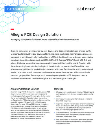
Allegro PCB Design SolutionManaging complexity for faster, more cost-effective implementationsSystems companies are impacted by new devices and design methodologies offered by thesemiconductor industry. New devices often bring more challenges, like increasing pin counts packagedin shrinking pin pitch ball grid arrays (BGAs). Additionally, new devices use evolving standards-basedinterfaces, such as DDR3, DDR4, PCI Express Gen3, USB 3.0, and others, that may require learningnew ways to implement them on the board. Coupled with these increasingly complex technologies isthe desire by companies to differentiate their offerings and get them to market faster, cheaper, withmore functionality and in reduced end product size. As a result, many companies now outsource toor partner with companies in low-cost geographies. To manage such increasing complexities, PCBdesigners need a solution that addresses their technological and methodological challenges.Allegro PCBDesign SolutionCadence Allegro PCB Designeris a scalable, proven PCB designenvironment that addressestechnological and methodological challenges while makingthe design cycles shorter andpredictable. Available in baseplus options configuration, thePCB design solution containseverything needed to createa PCB layout with a fully integrated design flow. The base—Allegro PCB Designer—includesa common, consistent constraintmanagement solution, PCBEditor, an auto/interactiverouter, as well as interfaces formanufacturing and mechaniFigure 1: Allegro PCB design solution brings together all the tools needed to design simple-tocal CAD. PCB Editor provides acomplex PCBscomplete placement and routing environment—from basic Eliminates unnecessary iterations Features a common, consistentfloorplanning, placement, andthrough constraint-driven PCBconstraint-management systemrouting to placement replication anddesign flowfor creation, management, andadvanced interconnect planning—forvalidation of constraints from frontsimple to complex PCB designs. Supports a comprehensive ruleto backset for physical, spacing, designBenefitsfor fabrication (DFF), design for Open environment for third-partyassembly (DFA), and design for testapplication improves productivity Offers a proven, scalable,(DFT), high-density interconnectwhile providing access to best-ofcost-effective PCB editing and(HDI), and electrical (high-speed)breed integrated point toolsrouting solution in on-demand basedomainsplus options configuration
Allegro PCB Design SolutionPCB Editor TechnologyConstraint-Driven PCB EditingEnvironmentAt the heart of Allegro PCB Designer isa PCB Editor—an intuitive, easy-to-use,constraint-driven environment for creating and editing simple to complex PCBs.Its extensive feature set addresses a widerange of design and manufacturabilitychallenges: A powerful set of floorplanning andplacement tools including placementreplication for accelerating placementof the design Powerful shape-based shove, huginteractive etch creation, editingestablishes a highly productiveinterconnect environment whileproviding real-time, heads-up displaysof length and timing margins Dynamic shape capability offersreal-time copper pour plowing andhealing functionality during placementand routing iterationsThe PCB Editor can also generate a fullsuite of phototooling, bare-board fabrication, and test outputs, including Gerber274x, NC drill, and bare-board test in avariety of formats.Constraint ManagementA constraint management system displays physical/spacing and high-speedrules along with their status (based onthe current state of the design) in realtime and is available at all stages of thedesign process. Each worksheet providesa spreadsheet interface that enablesusers to define, manage, and validate thedifferent rules in a hierarchical fashion.With this powerful application, designerscan graphically create, edit, and reviewconstraint sets as graphical topologiesthat act as electronic blueprints of anideal implementation strategy. Once theyexist in the database, constraints can drivethe placement and routing processes forconstrained signals.The constraint management system iscompletely integrated with the PCB Editor,and constraints can be validated in realtime as the design process proceeds. Theresult of the validation process is a graphi-www.cadence.comFigure 2: DFA rules-driven placement allows for compact placement of components withoutintroducing errorscal representation of whether constraintspass (highlighted in green) or fail (highlighted in red). This approach allowsdesigners to immediately see the progressof the design in the spreadsheets, as wellas the impact of any design changes.Floorplanning and PlacementThe constraint and rules-driven methodology of PCB design solutions includesa powerful and flexible set of placement capabilities, including interactiveand automatic. The engineer or designercan assign components or subcircuitsto specific “rooms” during design entryor floor- planning. Components can befiltered and selected by reference designator, device package/footprint style,associated net name, part number, or theschematic sheet/page number.With thousands of components comprising today’s boards, precise managementis critical. Real-time assembly analysisand feedback can facilitate this management—helping designers increaseproductivity and efficiency by placingcomponents according to corporate orEMS guidelines. Dynamic DFA-drivenplacement offers real-time packageto-package clearance checking duringinteractive component placement (seeFigure 2). Driven from a two-dimensionalspreadsheet array of classes and packageinstances, real-time feedback providesminimum clearance requirements. Basedon the package’s side-to-side, side-toend, designers can simultaneously placedevices for optimum routability, manufacturability, and signal timing.Placement ReplicationSuperior placement replication technologywithin Allegro PCB Designer allows usersto quickly place and route multiple similarcircuits in a design. It allows users to createa template using one instance of placedand routed circuit that can be applied toother instances within the design. Thesaved placement template can be usedwith other designs where similar circuitsare used. When replicating placement,users can flip or mirror the circuit from toplayer to bottom layer. All associated etchelements, including blind buried vias, aremapped to correct layers when circuit ismoved from top layer to bottom layer.Display and VisualizationThe built-in 3D viewer is available in allPCB Editor products. The 3D environmentsupports several filtering options, cameraviews, graphic display options such assolid, transparency, and wireframe, andmouse-driven controls for pan, zoom, andspinning the display. 3D viewing also supports the display of complex via structuresor isolated sections of the board. Multipledisplay windows can be opened using thecontext sensitive command structure, and3D images can be captured and saved inJPEG format. (See Figure 3.)The flipboard capability “flips” the designabout its Y axis inverting the design database in the canvas. This “flip” reorganizesthe display of the design such that whatwas displayed as top through to bottombecomes bottom through to top. Havinga true bottom side view from within theCAD system is essential for hardware2
Allegro PCB Design Solutionogy requirements—and it’s no wonderthat traditional CAD tools and technologies fall short of capturing a designer’sspecific routing intent and acting uponit. The Allegro Interconnect Flow Plannerprovides the technology and methodology to capture as well as adhere to adesigner’s intent. Through the interconnect flow planning architecture and theglobal route engine, users can for thefirst time put their experience and designintent into a tool that understands whatthey want—natively.Figure 3: Built-in 3D viewer allows reviewing of a section of the board or complex via structureswith pan, zoom, rotation, and spinning to reduce iterations with mechanical design teams or PCBfabricators without introducing errorsengineers when debugging a board in thelab, or for assembly/test engineers on themanufacturing floor. Flipboard is not justlimited to viewing; design edits can alsobe performed while in this mode.hours with traditional one trace at a time.Hug-contour option takes care of inserting traces with curves that are aligned tocontour of the flex portion of the design.(See Figure 4.)Interactive Etch EditingDesign Planning and RoutingThe routing feature of the PCB Editorprovides powerful, interactive capabilities that deliver controlled automation tomaintain user control, while maximizingrouting productivity. Real-time, shapebased, any-angle, push/shove routingenables users to choose from “shovepreferred,” “hug-preferred,” or “hugonly” modes.Highly constrained, high-density designsdominated by bussed interconnect cantake significant time to strategically planand route. Compound this with thedensity issues of today’s components,new signaling levels, and specific topol-Users create abstracted interconnect data(through the interconnect flow planningarchitecture) and can quickly converge ona solution and validate it with the globalroute engine. The interconnect abstraction reduces the number of elements thesystem has to deal with—from potentiallytens of thousands down to hundreds—resulting in a significant reduction in themanual interaction required.Using the abstracted data, the planningand routing process can be acceleratedby providing a visual/spatial map of theopen area in relation to the data and theuser’s design intent. The route engine canthen deal with the details of the routing,adhering to the specified intent, without the user having to both visualize andsolve the interconnect problems at once.This significant simplification over currentdesign tools means users converge on aDuring etch editing, the designer can viewa real-time, graphical heads-up display ofhow much timing slack remains for interconnect that has high-speed constraints.Interactive routing also enables grouprouting on multiple nets and interactivetuning of nets with high-speed length ordelay constraints.Multi-Line RoutingMulti-line routing allows users to quicklyroute multiple lines as a group on thePCB. Coupled with “hug-contour” option,this utility can help designers routemultiple lines on the flex portion of therigid-flex design in minutes instead ofwww.cadence.comFigure 4: Multi-line routing with contour hug option accelerates through no-click routing on flexsection of the PCB designs3
Allegro PCB Design Solutionsystem then provides feedback throughthe constraint manager if a signal doesn’tconform to the topology or the rules associated with the topology, ensuring thatissues are identified (and therefore can beaddressed) as quickly as possible.Figure 5: Allegro Interconnect Flow Planner technology allows users reduce layer counts andshorten design cycle through design planningsuccessful interconnect solution far fasterand more easily than ever before, reducing design cycle time through increasedefficiency and productivity. (See Figure 5.)Getting routes out of dense BGAs isincreasingly difficult for PCB designers.With increasing pin counts and shrinking pin pitches, the time PCB designersspend on getting routes in and out ofBGAs has gone up significantly. The traditional approach of performing breakoutsfirst then routing the traces between twoBGAs is running out of steam becauseresolving the resulting crossovers takes upa lot of time and board real estate.and easy. It offers an extensive range ofelectrical rules to ensure that the PCBdesign implementation is complaint withthe specification for advanced interfaces.Additionally, it allows users to extend therules through the use of formulas withexisting rules or post-route data such asactual trace lengths.The PCB High Speed Option allows usersto apply a topology to a set of signals.A topology can include a set of routingpreferences as well as constraints suchas putting the termination resistor closerto either the driver or a receiver on asignal. The constraint-driven PCB designAllegro PCB High Speed Option alsoenables checking of delays throughvias, connector pins, and IC packagepin for die 2 die length/delay matching. It includes, utilities to identify tracesegments crossing voids (return pathissues that cause re-spins), supports backdrilling (remove through hole antennas)as well as provides a Timing Environmentthat can accelerate timing closure of critical nets up to 60-70%.Accelerated Timing ClosureAs the data rates increase andsupply voltages decrease in today’sadvanced interfaces like DDR3/DDR4, PCIExpress, SATA, etc., PCB designers mustspend more time to ensure signals in aninterface meet timing requirements. Withincreasing density on PCBs, the effort toget to timing closure—ensuring all signalsmeet timing requirements—can increasesignificantly. PCB designers need newtools to meet this increasingly complexchallenge.AiBTAuto-interactive Breakout Technology(AiBT) improves user efficiency byallowing users to plan to break out onboth ends. AiBT can be used with thenew, Split View, and Bundle Sequencecommands to dramatically shorten thetime required to develop a high-qualityand properly ordered breakout solution(see Figure 6).High-Speed DesignIncreasing use of standards-basedadvanced interfaces such as DDR3, DDR4,PCI Express, USB 3.0 are bringing a set ofconstraints that must be adhered to whileimplementing a PCB.Allegro PCB Designer through itsHigh-Speed Option makes adhering toconstraints on advanced interfaces quickwww.cadence.comFigure 6: Split View allows working on both ends of a zoomed-in interface4
Allegro PCB Design Solutionto meet timing constraints and utilizescontrolled push/shove techniques whenadding tuning patterns (see Figure 7).BackdrillingAllegro PCB High-Speed Option allowsusers to specify which vias on criticalhigh-speed signals should be back drilledto avoid reflections. An output report—Backdrill NC and Legend Files fromBottom, Top, or Any Layer if backdrillingthe inner core(s) of the PCB—allows usersto send backdrilling instructions to theirPCB manufacturersDesign for ManufacturingFigure 7: AiDT shortens time to tune high-speed signals by 50% or more.Timing VisionTiming Vision is an innovative andunique environment that allows users tographically see real-time delay and phaseinformation directly on the routingcanvas. Traditionally, evaluating currentstatus of timing/length of a routed interface requires numerous trips to ConstraintManager and/or use of the ShowElement command. Using an embedded route engine to evaluate complextiming constraints and interdependencies amongst signals shows current statusof a set of routed signals—a DDRx bytelane or a complete DDRx interface—via custom trace/connect line coloring;stipple patterns and customized data tipinformation to define the delay problemin the simplest terms possible.With the embedded route engine,Timing Vision provides real-time feedback to the user during interactive editing and enhances the user’s ability todevelop a strategy for resolving timingon large buses or interfaces such asDDRx, PCI Express, etc. Coupled withAuto-interactive Phase Tuning (AiPT) andAuto-interactive Delay Tuning (AiDT)capabilities, users can accelerate thewww.cadence.comtime to tune advanced interfaces likeDDRx in one-third the time it takes to doit manually using traditional methods.AiPTDifferential pairs in an interface like DDRxrequire designers to match static as wellas dynamic phase. Matching phase for alldifferential pairs in an interface is a necessary first step before tuning and matchingthe rest of the signals. AiPT automaticallymatches dynamic and static phase forthe selected differential pairs. It workswith a set of parameters that allows theuser several options for trace lengthening or shortening as well as pad entry/exitoptions. With AiPT, users can significantlyshorten the time to match static anddynamic phases for differential pairs.AiDTDelay tuning for signals for interfaces likeDDRx takes up too much time when usingtraditional, manual methods. AiDT automatically generates tuning patterns on auser-selected routed byte lane or interfacebased on user-defined timing constraintsand tuning parameters. AiDT computesthe required length for the connectionsAllegro PCB Editor supports DFT, DFF,and DFA checks during the design implementation process. Users can select thenumber and type of probe points andpad sizes as well as define no-probe areasand create reports to check testabilitycoverage. Allegro PCB Editor providesa real-time DFA design rules check ascomponents are being placed with visualfeedback while the component is on thecursor.Design Data Transfer toManufacturingA full suite of phototooling, bare-boardfabrication, and test outputs, includingGerber 274x, NC drill, and bare-board testin a variety of formats, can be generated.More importantly, Cadence supportsthe industry initiative toward Gerber-lessmanufacturing through export and importof design data in IPC-2581 format. TheIPC-2581 data is passed in a single filethat creates accurate and reliable manufacturing data for high-quality manufacturing. Users have a choice to export asubset of the design data for protectingtheir IP. Import of IPC-2581 is intended foroverlaying artwork data on the design forviewing purposes only.MiniaturizationConstraint-Driven HDI Design FlowWith BGA pin pitches decreasing to below1mm, (0.8mm or lower with 0.65mmor 0.5mm pin pitches), users are forcedto implement a buildup PCB technologyusing HDI.5
Allegro PCB Design SolutionWhile miniaturization is not necessarily the primary objective in many marketsegments, the move to buildup technology is necessary for fanning out a BGA—particularly if it has three or four rows ofpins on each side.The Allegro PCB Designer through itsMiniaturization Option offers a provenconstraint-driven HDI design flow witha comprehensive set of design rules forall different styles of HDI designs, froma hybrid buildup/core combination to acomplete buildup process like ALIVH.In addition, it includes automation foradding HDI to shorten the time to createdesigns that are correct by construction.Embedded ComponentsReducing end product size can be accomplished in many different ways. One of theapproaches PCB designers are taking is toembed packaged components on innerlayers. Allegro PCB Designer through itsMiniaturization Option offers constraintdriven embedded component placement and routing. It supports direct- andindirect-attach techniques, and supportsembedding components with dual-sidedcontacts, vertical components, and embedding in dielectric on a two-layer PCB.Additionally it offers the ability to createand manage cavities on layers specified forembedding components.Analog/RF DesignThe Allegro PCB Designer through itsAnalog/RF Design Option offers a mixedsignal design environment, from schematic to layout with back annotation,proven to increase RF design productivityup to 50%. It allows engineers to create,integrate, and update analog/ RF/ microwave circuits with digital/analog circuitsin the Allegro PCB Design environment.With its rich layout capability and powerful interfaces with RF simulation tools, itallows engineers to start RF design fromAllegro Design Authoring, Allegro PCBDesigner, or Agilent ADS.www.cadence.comConcurrent Team DesignGlobally dispersed design teams are onthe rise, which compounds the challengeof shortening design cycle times. Manualworkarounds that address multi-userissues are time-consuming, slow, andprone to error.Allegro PCB Design Partitioning technology provides a multi-user, concurrentdesign methodology for faster time tomarket and reduced layout time. Multipledesigners working concurrently on alayout share access to a single database,regardless of team proximity. Designerscan partition designs into multiplesections or areas for layout and editingby several design team members.Designs can be partitioned vertically(sections) with soft boundaries or horizontally (layers). As a result, each designercan see all partitioned sections andupdate the design view for monitoringthe status and progress of other users’sections. Such partitioning can dramatically reduce overall design cycles andaccelerate the design process.PCB Autorouter TechnologyPCB routing technologies are tightly integrated with the PCB Editor. Through thePCB Router interface, all design informationand constraints are automatically passedfrom the PCB Editor. Once the route iscompleted, all route information is automatically passed back to the PCB Editor.Increased design complexity, density,and high-speed routing constraints makemanual routing of PCBs difficult andtime-consuming. The challenges inherent in complex interconnect routing arebest addressed with powerful, automatedtechnology. The robust, productionproven autorouter includes a batch routing mode with extensive user-definedrouting strategy control as well as built-inautomatic strategy capabilities.DFM Rules-Driven AutoroutingThe design for manufacturing capability within Allegro PCB Router significantly improves manufacturing yields.Manufacturing algorithms provide aspreading capability that automaticallyincreases conductor clearances on aspace-available basis. Automatic conduc-tor spreading helps improve manufactuability by repositioning conductors tocreate extra space between conductorsand pins, conductors and SMD pads, andadjacent conductor segments. Users gainthe flexibility to define a range of spacingvalues or to use the default values.Mitered corners and test points can beadded throughout the routing process.The manufacturing algorithms automatically use the optimal setback range,starting from the largest to the smallestvalue. Test point insertion automaticallyadds testable vias or pads as test points.Testable vias can be probed on the front,back, or both sides of the PCB, supporting both single side and clamshell testers.Designers have the flexibility to select thetest point insertion methodology thatconforms to their manufacturing requirements. Test points can be “fixed” to avoidcostly test fixture modifications. Test pointconstraints include test probe surfaces, viasizes, via grids, and minimum center-tocenter distance.High-Speed Constraints-DrivenAutoroutingHigh-speed routing constraints and algorithms handle differential pairs, net scheduling, timing, crosstalk, layer set routing,and the special geometry requirementsdemanded by today’s high-speed circuits.The autorouting algorithms intelligentlyhandle routing around or through vias,and automatically conform to definedlength or timing criteria. Automatic netshielding is used to reduce noise on noisesensitive nets. Separate design rules maybe applied to different regions of thedesign; for example, you can specify tightclearance rules in the connector area of adesign and less stringent rules elsewhere.Operating System SupportAllegro Platform Technology: Sun Solaris Linux IBM AIX WindowsOrCAD Technology: Windows6
Allegro PCB Design SolutionAllegro PCB Designer Base Plus Options FeaturesFeatureAllegro PCB DesignerAllegro Design Authoring Allegro Design Entry CIS Constraint Manager: Physical, spacing, and samenet rules Constraint Manager: Properties and DRCs Constraint Manager: Differential pair rules Constraint Manager: Region rules Floorplanning, placement, placement replication DFA, DFF, DFT Dynamic feedback on DFA compliance during placement IDF3.0, DXF in/out EDMD schema-based ECAD-MCAD co-design Native 3D viewer Hierarchical interconnect flow planning Length-based rules for high-speed signals Constraint-driven flow for length-based high-speed signals Match groups, layer sets, extended nets T-point rules (pin to T-point) 6-layer automatic shape-based autorouter High-speed rules-based autorouting Layer-specific rules-based autorouting Design planning - plan spatial feasibility analysis and feedbackDesign Planning OptionDesign planning - generate topological planDesign Planning OptionDesign planning - Convert topological plan to traces (CLINES)Design Planning OptionAuto-interactive Delay TuningPCB High-Speed OptionConstraint Manager: Electrical rule set (relection, timing, crosstalk)PCB High-Speed OptionConstraint-driven flow using electrical rulesPCB High-Speed OptionElectrical constraint rule set (ECSets) / topology applyPCB High-Speed OptionFormula and relationship-based (advanced) constraintsPCB High-Speed OptionBackdrillingPCB High-Speed OptionDie2Die pin delay, dynamic phase control, Z-axis delayPCB High-Speed OptionReturn path management for critical signalsPCB High-Speed OptionConstraint Manager: HDI rule setMiniaturization OptionMicro-via and associated spacing, stacking, and via-in-pad rulesMiniaturization OptionConstraint-driven HDI design flowMiniaturization OptionManufacturing rule support for embedding componentsMiniaturization OptionEmbedd components on inner layersMiniaturization OptionHDI micro-via stack editingMiniaturization OptionDynamic shape-based filleting, line fattening, and trace filletingMiniaturization OptionHug contour routing (Flex)Miniaturization OptionSupport for cavities on inner layersMiniaturization OptionConcurrent team design - layer-by-layer partitioningPCB Team Design OptionConcurrent team design - functional block partitioningPCB Team Design OptionConcurrent team design - team design dashboardPCB Team Design OptionConcurrent team design - soft netsPCB Team Design OptionEdit constraints in a partitionPCB Team Design OptionManage netclasses in a partitionPCB Team Design OptionParameterized RF etch elements editingPCB Analog / RF OptionAsymmetrical clearancesPCB Analog / RF OptionBi-directional interface with Agilent ADSPCB Analog / RF Optionwww.cadence.com7
Allegro PCB Design SolutionFeatureAllegro PCB DesignerImport Agilent ADS schematics into DE-HDLPCB Analog / RF OptionLayout-driven RF design creationPCB Analog / RF OptionFlexible Shape EditorPCB Analog / RF Option256-layer autoroutingPCB Routing OptionDFM rules-based autoroutingPCB Routing OptionAutomatic trace spreadiingPCB Routing OptionATP generationPCB Routing OptionLayer-specific rules-based autoroutingPCB Routing OptionCadence Services and SupportFor More Information Cadence application engineers cananswer your technical questions bytelephone, email, or Internet—they canalso provide technical assistance andcustom trainingFor product sales, support, or additionalinformation on Allegro solutions, visitwww.cadence.com/contact us to locatea Cadence Sales office or channel partnerin your area. Cadence certified instructors teachmore than 70 courses and bring theirreal-world experience into the classroom More than 25 Internet LearningSeries (iLS) online courses allow youthe flexibility of training at your owncomputer via the Internet Cadence Online Support gives you 24x7online access to a knowledge base ofthe latest solutions, technical documentation, software downloads, and moreCadence Design Systems enables global electronic design innovation and plays an essential role in thecreation of today’s electronics. Customers use Cadence software, hardware, IP, and expertise to designand verify today’s mobile, cloud, and connectivity applications. www.cadence.com 2014 Cadence Design Systems, Inc. All rights reserved. Cadence, the Cadence logo, and Allegro are registered trademarks of Cadence DesignSystems, Inc., All rights reserved.2106 02/14 SA/DM/PDF
Allegro PCB Design Solution Cadence Allegro PCB Designer is a scalable, proven PCB design environment that addresses technological and method-ological challenges while making the design cycles shorter and predictable. Available in base plus options configuration, the PCB design solution contains everything needed to create a PCB layout with .