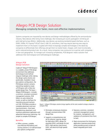
Transcription
PCB Designers
PCB DESIGNERSPCB DESIGNERSPCB Designers have exciting careers. Technology is constantly changing and engineers will always have another day of work. Get onthe fast track to efficient, scalable growth and become an expert PCB Designer. Try Altium Designer software and try new thingsbecause benefits to the Unified Data Model Approach include not just time savings, but the potential of simultaneous design that isavailable with the integrated schematics. Here we have a collection of PCB design articles related specifically to PCB Designers andwhat the job market looks like today, from a variety of angles, such as:Implications of Growing Automotive PCB Market Share for PCB DesignersPCB Designer Responsibilities: How to manage Engineering and Manufacturing expectationsHow to Become a PCB Designer in Today's WorldWhat Does it Take to Be a PCB Layout Designer?www.altium.com
PCB DESIGNERSTHE IMPLICATIONS OF GROWING AUTOMOTIVE PCB MARKET SHARESFOR PCB DESIGNERSLuxury used to mean heated seats, now it means a self-driving car with a 17” LED display in the dashboard. With automotive PCBsgaining market share, the modern designer should start thinking about how their designs can enable essential and luxury features inconnected cars. They should also get ready to learn cutting edge design techniques such as rigid-flex and HDI in order to meetautomotive requirements.Do you remember the “dynamic duo” days they used to do back in school? My friend and I always dressed up as the classic Batmanand Robin. I was Batman, of course. Albeit a Batman with no Batmobile and a 90’s homemade utility belt - no wonder I couldn’tconvince any girls to be Catwoman. For engineers, the Batmobile represents a different dynamic duo that is becoming moreprevalent as technology advances: PCBs and cars. Luxury in a car used to mean heated seats, now it means PCBs driving for you anda 17” LED display in the dashboard. Sadly no one has integrated jet engines into their cars yet. With automotive PCBs gaining marketshare, the modern designer should start thinking about how their designs can enable essential and luxury features in connectedcars. They should also get ready to learn cutting edge design techniques such as rigid-flex and HDI in order to meet automotiverequirements.www.altium.com
PCB DESIGNERSI think this will be my next ride. Editorial credit: Rubens Alarcon / Shutterstock.comACCELERATING MARKET SHAREGadzooks Batman, that market is growing so quickly, it’s going to explode! The connected car market is on the rise, and theautomotive PCB market is expanding with it. That means you’ll soon be designing as many PCBs for cars as for IoT devices.Futuristic cars used to be reserved for millionaires and comic book superheroes, or millionaire comic book heroes. Now everyonewants one. It’s estimated that by 2020 75% of cars will be connected. That translates into approximately 250,000,000 connected carson the roads. With many modern cars using upwards of 70 microprocessors, a lot of PCBs will need to be designed.Not only do modern cars need lots of PCBs, they’re also willing to pay for them. In 2015 more than 50% of a car’s cost could be madeup of electronics. That number is now pushing 70% in 2017. The money in cars is quickly shifting from metal to microcontrollers. Youcould be there to cash in.www.altium.com
PCB DESIGNERSTesla is spoiling us with a full-size computer monitor in the dashboard. Editorial credit: Kaspars Grinvalds / Shutterstock.comCONNECTED CAR FEATURESThroughout the ages, the Batmobile has sported a variety of gadgets, from smokescreens to rockets. Today’s car also has a widevariety of special features designed to entice customers and appease regulators rather than defeat villains. The features you canexpect to design fall into five general categories: engine, powertrain, body, infotainment, and power.Engine and Powertrain: These are the kinds of processes you don’t see that keep your car going. Pistons, spark plugs, differentials,transmission, all things I know about without knowing exactly how they work. The electronics governing these systems will haverigorous safety requirements, so prepare for headaches. Engine and powertrain PCBs will be pushing a combined market shareof 4 billion by 2020. I think I could delve into certification requirements for that kind of money.Body: Body electronics are things like Tesla’s neat automatic door handles. They could also be things like sound cancelingsystems and, Mr. Freeze’s nemesis, seat warmers. These electronics are estimated to be worth close to 3 billion by 2020.Infotainment: Back in my day we rigged up a tiny CRT TV with included VCR to watch movies in the car. Now kids each get their ownseatback screens. If you design PCBs for these kinds of systems you could enable children everywhere to watch Batman and Robin.Infotainment PCBs will be worth a whopping 1 billion in 2020.Power: Last but not least the category that’s a game changer for the automotive industry, power electronics. While no one is quitesure how fast the market for electric vehicles (EVs) is growing, they know it is indeed growing. As battery costs fall and energydensities rise, we can expect to see more and more cars using electric motors. That means they’ll need designers like you to makebattery management systems, charging boards, etc. for this 800 million market.www.altium.com
PCB DESIGNERSFUTURISTIC DESIGN TECHNIQUESSadly futuristic cars need futuristic PCBs, which will require you to learn next generation design techniques. What with all the PCBsand wires going into cars now, manufacturers are running out of space inside cars. What is the solution? Small PCBs that can fitanywhere, A.K.A. high density interconnect (HDI) and rigid flex. Strict EMI requirements in cars will also require you to master EMIdesign.Even though you might hate mastering the techniques needed to shrink PCBs, car manufacturers will love how small you can makeHDI boards. In order to truly master HDI, you’ll need to become familiar with a variety of vias and efficient fanout strategies.If you want to jam a PCB into some hidden space in a car, chances are it will need to be flexible. You may not be ramping your carinto the Batcave, but potholes and speedbumps will still cause dynamic forces to act on your PCBs. A flexible PCB won’t snap apart ifany Jokers try to ram your car.This wouldn’t be a good PCB article if I didn’t touch on my favorite topics, EMI and smart forks. Lucky for you, this time we are onlygoing to discuss EMI. Cars are semi-closed systems, and as such have strict EMI requirements. That means you’ll need to think aboutthings like routing differential pairs, good grounding, and separating AC/DC signals.WHERE TO GO FROM HEREThe electronics in cars nowadays may make you feel like a millionaire vigilante. Just one that conquers boring commutes instead ofcrime. If you want to capitalize on the rapid growth of the automotive PCB industry, you’ll need to know thine enemy. Look at all thedifferent systems and features, and focus on which kind you want to design. You might want to then brush up on your advanceddesign techniques in order to meet the industry’s strict requirements.If you’re going to do all this in a reasonable amount of time, you’ll need some good software to help you. CircuitStudio is on thecutting edge of design and already has documentation to help you learn its more advanced features.Have more questions about how to build the Batmobile? Call an expert at Altium.www.altium.com
PCB DESIGNERSPCB DESIGNER RESPONSIBILITIES: HOW TO MANAGE ENGINEERING ANDMANUFACTURING EXPECTATIONSMy wife works at an elementary school, and the thing she dislikes the most is when she has to put herself between two kids in anargument. Being caught in the middle like that is frustrating for her because it is often difficult to turn it into a “win” for both sides ofthe argument.We as PCB designers are often in the same position when we have to mediate the needs of electrical engineering and mechanicalengineering. Trying to negotiate a “win” for both sides can be one of the most difficult things that we have to do. We are the “noman’s” land between two sides of a war, and it is our job to come up with an amazing board design that satisfies both sides. To dothat we need to find ways to get both sides working together. Here are some ideas on how we can best do that.IMPROVE COMMUNICATIONSThe first thing that we can do to help the relationship between electrical engineering and manufacturing engineering is to improvecommunications between them. I know that it’s tempting to avoid the conflict by burying our heads in the sand and focus on routingtraces. Ultimately though, our goal is to produce the best design possible. The only way we are going to be able to do this is to getthese two groups communicating instead of fighting against each other.Encouraging participation in the design process by both groups is a great way to improve communications. I have seen companieswhere people felt unattached and left out of the design process resulting in an “us versus them” mentality. This usually happenswww.altium.com
PCB DESIGNERSbecause the people don’t know each other, are unsure of who has what responsibilities or are blocked by antiquated corporatepolicies.To open up communication in situations like this, get these people involved. Ask for their opinions on what you are doing, and makesure that regular design reviews are scheduled. If someone isn’t part of the review that should be, get them on board. Finding outthat a design failed due to a missed detail because a key person was absent during the design process is a tragedy. On the otherhand, I’ve personally experienced the success that you can have when all team members are freely giving input during the design.DOCUMENT THE DFM PROCESSESAnother way that you can help the relationship between electrical engineering and manufacturing is to make sure that yourcompany’s DFM processes are documented. This way everyone has a clear understanding of what the design objectives are.There is a vast difference in how the design for manufacturing (DFM) processes are documented amongst companies. Some are verydetailed and available online, or in some sort of printed format. The designs at these companies are often gated to the DFMdocumentation and won’t be released without the proper authorization. Then on the flip side, there are those companies who havelittle if anything in the way of documented DFM practices. If DFM practices are followed at all it is usually in the form of “tribalknowledge” based on previous manufacturing experiences.So how can you help in this documentation process? First of all, make sure that you are fluent with your company’s current DFMdocumentation. If your company doesn’t have any DFM processes documented, start working on them yourself. A good place to startis by collaborating with your company’s manufacturing engineers or your manufacturing vendors. Researching industry establishedmanufacturing specifications is another good way to gather information. The important thing is to start capturing these standardsand get them documented. Even if all you do is to just create some simple “bullet-points” in a text document, it’s a good place tostart.The key is to get everyone working together instead of against each otherwww.altium.com
PCB DESIGNERSCHECK FOR DFM COMPLIANCE IN DESIGN BEFORE GOING TOMANUFACTURINGEven by following the rules, there can still be some DFM errors that get missed in design. Because DFM checking is traditionally donein manufacturing, electrical engineering usually isn’t aware of those errors until notified by manufacturing. With the design beingkicked back and forth between groups for checking and correction, there is yet another opportunity for friction betweendepartments.With DFM checking tools readily available, you should run these checks first before you send the design to manufacturing. Some PCBdesign tools have DFM checking functionality built into them in addition to their regular DRCs. There are also plenty of third-partychecking tools available as well. By participating in the DFM checking, your electrical engineers can learn what manufacturing islooking for and correct those problems before they get to the manufacturing floor. Not only will this save the time and money thatwould be spent on bad boards and re-designs, but it will also help in getting everyone working together.USE AN ONLINE PCB BILL OF MATERIALSAnother great way to improve cross-departmental communications is for all departments to have live access to an online PCB bill ofmaterials. Manufacturing can use it to plan ahead for parts in upcoming designs. Engineering can see real-time stock inventories andpost online part requests. BOM management tools can provide this online service which will eliminate the time, errors and waste oftraditional paper documentation processes.As designers we have a big job ahead of us trying to satisfy the requirements of both electrical engineering and manufacturingengineering. Fortunately though there’s a lot of help out there for us to successfully negotiate a win for both sides of this conflict.PCB design software, like Altium Designer, has enhanced features that can help you design for DFM compliancy. Would you like tofind out more about how Altium can help your design needs? Talk to an expert at Altium.www.altium.com
PCB DESIGNERSHOW TO BECOME A PCB DESIGNER IN TODAY’S WORLDWhat did you want to be when you grew up? When I was a kid, I wanted to be Scotty on Star Trek. No joking, I really did. The idea thatsomeone could fiddle around with electronic parts and blinking lights to create some gizmo that would save the day was reallyappealing. A few years later I tried to imitate Scotty by taking all the parts for a kit radio and soldering them together on a thin sheetof wood. Without realizing it, I had designed my first circuit board at the wise old age of 12 years old.How about you? Have you ever thought about being a circuit board designer? Perhaps you are already in school and headed for anengineering degree. Or maybe you’re an electronics technician or you are doing some kind of CAD drafting. Maybe you’re not even inthe electronics industry, but the idea of becoming the next Scotty sounds really good to you.If any of this has caught your interest, keep reading. I’ll tell you a little bit about what it means to be a PCB designer, what kind ofeducation will help you, and what the future holds for our industry. You may never become an expert in warp drive on a starship, butyou may find out that you have a talent for designing a circuit board.WHAT EXACTLY IS A PCB DESIGNER?Printed circuits became popular in the 1950s and the need for PCB designers to create those circuits took off. Originally circuitboards were designed, or “laid out,” on a drafting board at four or even ten times the actual size using tape, knives, stickers, and asteady hand. When completed, those drawings would be recreated on film using a reduction camera, and that film would be used towww.altium.com
PCB DESIGNERSmake the PCB tooling at the fabrication shop. Today PCB layout is done on advanced Computer Aided Design systems (CAD), andtheir output is used to create the PCB tooling.The PCB designer will create the library models (footprints) for the parts that will be included on the print circuit board within theCAD system. Then the designer will create the circuit board design within the CAD system using the footprints that have beencreated. Once all of the required footprints have been placed on the board, the designer will connect all of the electrical connectionsusing lines that represent metal in a process called trace routing.A good PCB designer is part electrical engineer, part manufacturing expert, and part computer guru with a smidge of processengineer thrown in the mix as well. Mostly though, a PCB designer has to have the ability to see beyond the lines and shapes ofcomponents on their computer screen in order to visualize where the design is headed. A good PCB designer can create somethingfrom nothing while solving many different puzzles along the way.Many companies are now requiring degrees for PCB design positionsWHAT KIND OF EDUCATION IS REQUIRED TO BE A PCB DESIGNER?Many engineers are laying out their own printed circuit boards today. To become an electrical engineer or a mechanical engineeryou will need a BS in those related fields. Traditionally though, PCB designers are those who do the layout of the board only withoutdoing any of the engineering of the board.For those who are doing PCB layout only, there isn’t much out there in the way of a degree specifically in PCB layout. You will alsofind that there are still many positions that do not require the PCB designer to have a degree of any kind. However, you will havemuch better success as a PCB designer if you have a degree that includes courses in drafting, computer-aided design, electronicdesign, or other related areas of study. As PCB designs become more complex, more companies will begin to require degrees forwww.altium.com
PCB DESIGNERStheir PCB designers.There are many certificate courses that are very helpful for the PCB designer. Some companies offer specific PCB design and CADtraining classes. There is also the IPC Certified Interconnect Designer (CID) course which is an absolute must for the new PCBdesigner.The future is bright for PCB designWHAT IS THE FUTURE FOR THE PCB DESIGNER?The need to design current and evolving PCB technologies is growing. With more and more electronics such as IoT becomingeveryday parts of our lives, the future of electronic design is very bright. However, the pool of experienced PCB designers is shrinkingas many designers are approaching the age of retirement. The industry needs more PCB designers, and those that are currentlyinvolved are reporting that their compensation and job satisfaction is on the rise.Do you have a passion for creating things and making them work? If so, then designing printed circuit boards may be what you arelooking for. If you are ready to start a career as a PCB designer, take a look at Altium. Altium Designer is PCB design software that ismade for engineers and PCB designers to create world-class PCB designs. Not only will the software help you with all aspects of yourdesign, but Altium offers training on its software that will help you to hit the ground running.Would you like to find out more about how Altium can help you to step into the world of PCB design? Talk to an expert at Altium.www.altium.com
PCB DESIGNERSWHAT DOES IT TAKE TO BE A PCB LAYOUT DESIGNER?In the movie “Men of Honor,” Robert De Niro portrayed Billy Sunday, a Navy diving instructor with a challenging pedagogical method.He motivated his student divers by describing how hard their job would be to prepare them for the difficulties of their tasks. Heconcluded his speech by saying, “I don’t know why anybody would want to be a Navy Diver.” His honesty, in this case, wasn’t intendedto be demotivating—sometimes a job takes a certain type of person, one who is willing to do work that others won’t.There have been days that I’ve thought the same thing about my own career: “I don’t know why anybody would want to be a PCBlayout designer.” But even with the adversity, I only have to remind myself that I can and am doing things with my skills that mostother people can not. My experience and visually-oriented mind can imagine how components need to be arranged on a circuitboard in order to create an efficient design. Furthermore, I know how to use the tools at my command to connect the componentsand make the circuit board function as it should.The job can be challenging and demanding at times, and most of the people you know and interact with won’t have much of a clue asto what it is that you are actually doing. But on the other hand, you will get to experience an incredible feeling of accomplishmentwhen you see your design working as it was intended. I don’t know why you would want to be a PCB layout designer—only you canknow that reason, but I imagine that you’re here because you’re interested in pursuing and finding creative solutions for difficultdesigns. So dive in, and if you find your treasure then you know you’re in the right field.COMMON CONFUSIONS OVER PCB LAYOUT DESIGNERSIt never ceases to amaze me how often people misunderstand what it is that I do. Especially when I describe myself as a “PCBDesigner,” it is not unusual to get a blank stare in return. Even my coworkers don’t always seem to have much of an idea as to what itis that I do, or am doing when I complete my work. There are others who have point blank demanded I tell them why in the worldanyone would want to do something like this.www.altium.com
PCB DESIGNERSMuch of my job appears to just be moving lines and shapes around on a computer screen, to the untrained eye; however, I promise,to anyone wanting to know more about what the PCB designer they work with does, this is hardly a game. We’re not ‘creative timewasters,’ and we’re not relics from an older system. Being able to effectively assuage these concerns, too, is part of the jobexpectations for a PCB layout designer.Most people have no idea what a PCB Layout Designer actually isTHE ATTRIBUTES OF A PCB LAYOUT DESIGNERUnlike in video games where you can minimize and maximize your attributes to focus solely on the skills you need, being a PCBdesigner requires some of the most diverse combinations of skills that I know of. A large part of the designer’s role is to utilize theircreative thoughts to problem solve board design challenges; however, this creativity is only enabled if a layout designer has thetechnical capacity to enact their ideas. Here is a list of what I find to be important traits:1. Great attention to detail: When your job entails trying to map solutions to minor adjustment changes, or has you working withmaterials that don’t fill your whole palm, you need to be able to focus on the details.2. Keeping up-to-date on industry trends: In an industry where new technology is constantly popping up, and new software isenabling more efficient and smart design solutions, ignoring industry trends will mean more work for you down the line.3. Learning new design techniques: While this seems to be one of the most common-sense needs for a PCB Layout Designer, itcan be easy to make a habit of your layout designing by finding a few techniques which work and applying them to yourlayouts. But this may encourage continuous errors, or enable new errors to pop up as your layouts become more complex.4. Long hours: Just like with any job, it is good to keep a strong idea of what you need to get done, and when it needs to getwww.altium.com
PCB DESIGNERSdone. But sometimes, even with the best priority management, you will have to complete designs and work extra hours tomeet deadlines.5. Common ground problem solving: The biggest wrench in many of these plans is the amount of time a layout designer willspend managing others and managing design demands from multiple sources. As a designer, you will need to manage andbalance those that you work with. Often you will be the rope in a tug-of-war between engineering and manufacturing, and itwill be up to you to find a solution that will satisfy both sides.HERE'S THE TREASURE AT THE BOTTOM OF THE OCEANAfter everything that I’ve said so far, you may also be wondering why anyone would want to be a PCB layout designer. It still might notbe for you, but these are some reasons why I love PCB layout design:Your work will challenge you: Designing a circuit board so that it meets the manufacturing specifications and works as it isintended will keep you on your toes.You will be exposed to new ideas: Technology is constantly changing, and you will always looking at better ways to accomplishyour task.Decent working conditions: More than likely, you won’t be designing boards outside in the rain or snow. While that might notbe everyone’s goal, it certainly is one of mine.Good salary: Most PCB layout designers make a good salary, and it isn’t uncommon to make a great salary. While I can’t givespecific numbers, I hope these superlatives can offer some guidance.Seeing what you create come to life: One of the greatest joys that I have is in seeing the designs that I create come to life inthe products that my company markets. There is nothing better than seeing an appliance, computer, or cell phone workbecause it contains a PCB in it that I’ve designed.Creating hardware: Although most people won’t understand what it is that you do, most everyone will be impressed whenyou can show them what you’ve created. I have a wall at home where I’ve hung examples of some of my PCB designs, and Ialways get questions about what they are and what I do. It is no small joy of mine to tell their stories.www.altium.com
PCB DESIGNERSSome of the largest challenges you'll face will feel like the most rewarding to complete.I am a PCB layout designer because I love it. I get to do something every day that is challenging, fulfilling, and rewarding. How aboutyou? Are you ready to step into the world of PCB design and enjoy the same experiences that I have described? If you are, then youwill need to work with design tools that can enable you to be successful from the start.PCB design software, like Altium Designer, is intuitive for the entry level designer and powerful enough for the veteran designer.Whichever end of the experience spectrum that you are at, Altium Designer can help you to be a success.Find out more about how Altium can help you by talking to an expert at Altium.ADDITIONAL RESOURCESThank you for reading our guide for PCB Designers. To read more Altium resources, visit the Altium resource center here or join thediscussion at the bottom of each original blog post:Implications of Growing Automotive PCB Market Share for PCB DesignersPCB Designer Responsibilities: How to manage Engineering and Manufacturing expectationsHow to Become a PCB Designer in Today's WorldWhat Does it Take to Be a PCB Layout Designer?www.altium.com
Here we have a collection of PCB design articles related specifically to PCB Designers and what the job market looks like today, from a variety of angles, such as: Implications of Growing Automotive PCB Market Share for PCB Designers PCB Designer Responsibilities: How to manage Engineering and Manufacturing expectations