Transcription
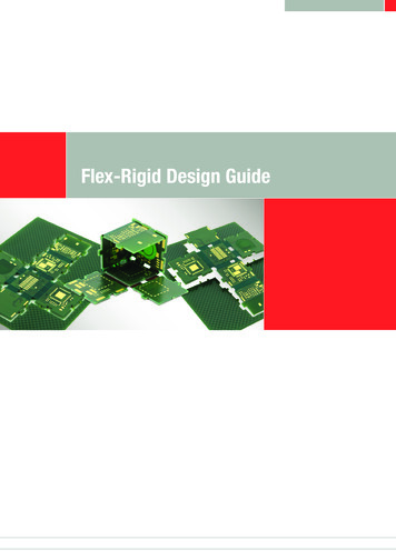
Flex-Rigid Design Guide
The trend to miniaturization in electronics continues. Integrated circuitboard solutions are becoming more and more popular as a means of efficiently utilizing the even smaller casing volume in all three dimensions.In the following, you will find information about systems thatexplain the different variants of flex-rigid circuit boards as wellas practical tips on design:Flexible foils of polyimide with a typical thickness of 50 µm are materialsthat withstand high temperatures and can be used with copper-claddingas base material for pure flex circuit boards or in combination with rigidbase materials for flex-rigid circuit boards with all the prevalent soldering methods. Thin FR4 layers in FR4 Semiflex circuit boards are alsobendable.1. Systematic view of flex-rigid circuit boards2. Project checklist for system requirements3. Selection of the right technology4. Materials and design parameters5. Mechanical design6. Layout and routing7. Documents for manufacturing flex rigid circuit boardsIn recent years, Würth Elektronik has accumulated extensive expertise incostumer projects and commissions of the widest variety ofdesigns and applications, from Aerospace to Medical devices andcurrently it supplies more than 600 customers. With the broad range oftechnology we offer, you can make the best possible selection for anyrequirements in terms of performance and costs.1. Systematic view of flex-rigid circuit boardsThere are basically different ways to create a system:Homogeneous systemHeterogeneous systemPCB1PCB1PCB2PCB2PCB1PCB1Partially homogeneous systemPCB2PCB1PCB24-layersHDI 10-layersPCB2PCB1PCB1PCB2Rigid circuit board wiring harness/flex soldered in or plugged (detachable)Circuit boards with identical stack-up inall rigid areas Only Integratedfew connections Non-critical applications Wiring errors possible Many single parts High expenses for test and assemblyflex layer(s) throughout Considerably greater wiring density Saves valuable space by eliminatingconnecting points (solder pads or footprintof connectors)Sub-systems vary considerably in termsof technology and size: e.g. flex-rigid/connector combination Separable Modularsystems possibleTIPS: Integrated wiring should be providedfor the smaller and simpler PCB1. For pitch 0.5 mm or shieldinga Board-to-Board connector isrecommended. 02PCB2
Flex-rigid circuit boards are mechatronic components. In addition to their electronic function, very careful consideration mustalso be given to mechanical factors:The design phase decides the later cost structure, so all electrical andmechanical interfaces must be taken into consideration during the conceptual phase.Comp. AComp. BComp. AComp. B Comp. CComp. CComp. DComp. E2DComp. D3DComp. E ComponentAn exact selection of the best components and substrate technology isalso necessary in order to be able to fulfill reliably the required operatingconditions. Product development also includes getting a precise pictureof component assembly, the soldering process, the test and the deviceassembly.Advantages:Cooperation of all participants of the value-added chainassembly, soldering and testing in flat condition in thedelivery panel Separating, configuring and installing Significantlyless space required due to three-dimensional wiring Elimination of additional components such as connectors andconnecting cables Improved signal transmission through elimination of cross-sectionalchanges to conductors (connectors, cable, solder connections) Weight reduction More valuable component assembly and wiring space Reduced logistical complexity Solution of difficult contacts is possible, simplification of assembly Considerably improved reliability of the entire system (a homogeneous unit is considerably more reliable than one with connectorsand cable) Combination with HDI Microvia technologies (microvia, buried via,finest conductor width) is possible Combination with heatsink technology is possible Remarkable improvement of testability. Complete system could betested prior to system assembly. All components and test points arestill accessable.„The benefits come from the systemnot through purchasing!“Andreas SchilppPCBproductionproductdevelopmentassemblyand testFlex/flex-rigid projects: Interdisciplinarycooperation in development is indispensable!03
2. Project checklist for system requirements:a) Technical requirements for the final product: target market,key functions, any unique features, service life, size, appearanceb) Commercial requirements: quantities, cost goals, prototypeschedule, pre-series, series release, ramp-up, second source, possible audit planningc) Legal requirements: listings and permits, regulated medical technology market, relevance for German Federal Office of Economicsand Export (BAFA), ULg) Mechanical requirements of circuit board: static or dynamicapplication, circuit board thickness, stability, aspect ratio of drill holediameter/board thickness, bending radii, bending radius/flex thicknessratio, bending form, number of bending cycles, bending frequencyh) Electrical requirements of circuit board: power, dielectricstrength, amperage, insulation and shielding, EMC, number ofsignals across the flexible area, number of flex layers, signal integrity,impedance requirements, surface resistanceNumber of flex layers124681012Flex/TWINflexd) Reliability requirements: For example classification to IPC 1/2/3,failure risk analysis, product liability, quality management agreement,branch specific requirements e.g. APQP (Advanced Product QualityPlanning) or PPAP (Production Parts Approval Process), traceabilityFlex-rigid flex outsideFlex-rigid flex insideFR4 Semiflexflex cores not gluedi) Type and positioning of components, design and connectiontechnology: components such as BGA requiring advanced via teche) Product operating conditions: ambient conditions such as tem-nology, stackup, bare chip technology, soldering surface, deliveryperature, temperature change, cooling, humidity, shock and vibration,panel, legend print, press-fit technology, embedded componentsnon-flammability, component assembly/soldering/repairs, test procedures for environmental and reliability testsj) Testing and Packaging: electrical and mechanical test of thecircuit board, product testing documentation (detailed initial samplef) Casing size, material and shape: analysis of all mechanical andtest report is recommended for complex stack-up, specify testelectrical interfaces, displays, switches, connectors, interfaces withcriteria), packagingother devices or modules. Design of a three-dimensional model(paper scissors / mCAD eCAD) in order to find minimum area fork) Further processing of flex and flex-rigid PCBs: possibilities offlat projection of the circuitrydrying prior to soldering, logistics, dry storage, panel separation,casing assembly, installation tolerances and fastening possibilities04
3. Selection of the right technologyPossible variants:Flex / TWINflex Flex-rigidFR4 Semiflex2F (Flex)1F-3RiSemiflex 1Ri-3Ri2F-Ri (TWINflex)2F-2RiSemiflex 2Ri-4Ri4F with microvias 1-2/2-3/3-43Ri-2F-3Ri Verythin flexible foil PI /LCP 1 to 6 copper layers Partially reinforced with stiffener Photosensitive solder mask foil orPolyimide coverlay Delivered individually or as panel Rigid3Ri-8F-3RiNOTE:Flex-rigid 1F-0Ri design can be moreaffordable than a TWINflex 1F-RiIn comparison:1F-Ri (TWINflex) Componentsstiffener1F-0Ri (flex-rigid)FR4 coreon stable rigid section Flexible area 1 to 12 layers bonded/unbonded (airgap) Flexible Polyimide layers out-sideor symmetrically inside Rigid areas: standard soldermask Flexible area: highly flexiblesoldermask or Polyimide coverlayFR4 circuit boards with deepmilling process Affordable Clearly defined installation situationand large bending radius Bending area: 1 or 2 copper layers,flex soldermask or Polyimide coverlayNOTE: Often more affordable than aconnector-cable-connector solution Definitely better and cheapercompared to shielded connectorand cables Usage of bending tools recommended05
Indicators for preferential use of individual variants:VariantFlex xFTWINflex xF-RiFR4 SemiflexFlex-rigid 1F-xRiFlex-rigid 2F-xRiFlex-rigid xRi-1F-xRiFlex-rigid xRi-2F-xRiIndicators forCommentsVery small, dense circuitsMicrovias and contour possible with laserVery limited installation spaceFlexible foil 50 µm thickUse in vacuumPractically no gas emissionUse at high temperaturesPI can be used up to 200 C (without solder mask)High frequency applicationsGood thickness tolerance, copper treatment flat, small loss factorVias in flexible areaBut NOT permitted in bending area!Cooling problemMetal reinforcement (heatsink)Flex-to-install with large bending radiiAffordable solution, miniaturizationLarge board with angled connectorOnly bendability is necessaryFlex material not permittedOnly rigid base materialsLarge portion of flex surfaceLaser-cut panel very stable1:1 wiring across flexible areaMore affordable than xRi-2F-xRiSmall bending radiiThin flexible area, highly flexible soldermask or cover foilShort drying timesFlex layer on outsideHigh-frequency component-to-connector connectionacross flexible area with reference layerNo vias necessary for transfersWARNING: complex (see table below)Highly-dynamic prolonged bendingCopper in neutral phase idealHigh-level reliability requirements-Reference layer in flex area due to signal integrityPolyimide with 75 or 100 µm for impedance controlHigh-level reliability requirementsRugged technology, mechanical stabilityIndicators against the use of individual variants:VariantIndicators againstCommentsFlex xFWired components or connectorsLow mechanical stabilityTWINflex xF-RiMany individual reinforcementsBetter to use flex-rigid 1F-xRiS-shaped bending in one surfaceDo not subject glass mat to tensionFR4 SemiflexFlex-rigid 1F-xRiFlex-rigid 2F-xRiFlex-rigid xRi-2F-xRiMulti-section casingAssembly tolerances have effect on Semiflex area--Large circuit boardsDesign tends to bow and twistLarge quantitieslimited area, tends to be expensive--4. Materials and design parameters - standardsIPC class 2, use A (flex-to-install)Flexible materialPolyimide core 50 µm, up to 70 µm copper, epoxy glue or adhesiveles, coverlay 25 µm partially or flexible solder maskRigid materialTG 150 FR4 filled, halogen-free: IPC-4101C /128 (92,94,127)Copper thicknessesInner layers 18(standard)/35/70 µm base copper, outer layers 12(standard)/18/35 µm plating ( with 1F-xRi flex layer is outside)Circuit board thicknessDepends on number of layers: flex 100 µm, flex-rigid/FR4 Semiflex 0.8 mmSolder surfaceENIGEnhanced specifications, e.g. regarding material, stack up, application case Use B, on request!06
5. The mechanical design Flex-rigid: Use„key and slot designs“ or plastic retaining frame Alwaysprovide large contour radii (inner and outer radii) in theflexible areas (design suitable for plastic) Provide registration drill holes for bonding reinforcements orheatsinks, if necessary Arrange flex extensions to save space, if necessary combinemultiple extensions, use fold technologyfolded to final shape Flexlift-off technique Flex-rigid: componentsand connectors always on rigid areas Contacts for ZIF connectors: standard thickness 0.3 mm 0.05mm, handling aids/precise laser contour possible Calculationof flex lengthflex length Lthickness Tcase 1case 2case 3case 4Rdistance Adistance B Withflex-rigid and inner layer is flex, changing to outer layer bymeans of vias near to the ZIF area is recommendeddistance CL A π · R 2 (T – R)L A R (π – 2)L A T R (π – 2)L B C T R (½ · π – 2)A 2RA T 2RB C T 2RGeometric conditions:A 2T 2R Withshort flexible areas, four bonded flex layers are easier to bendthan 2 2 flex layers with airgap Designbending radii based on flex thicknessBending radius [mm]1234Flex area 1-layerthickness x 10Flex area 2-layersthickness x 10Flex area 4-layersthickness x 10567IPC-2223: Use AFlex-to-installtight radius causingcompression of innerflex layersFR4 Semiflex07
6. Layout & RoutingFeatures and recommendations for flex-rigid circuit boardsFor IPC-2223 „Use B“ (continous flexing) andUse D (UL recognition), be sure to consult withour specialists! Extra layer is necessary for defining flexible and rigid areasCGR 1 mm7. Documents for the flex-rigid circuit boardG Includeall applicable points from the checklist. Define what is more important: drawing or data. Electrical data(Gerber/ODB , CAD data) already contain all geometric dimensions. No overspecification: a good drawing shows flat projection of thecircuit (2D), a 3D view of the installation situation and criticaldimensions only. Any redundant measurement on the drawing mustbe compared with electronic data, and any discrepancies willinevitably result in clarification, delays and additional costs. Specify materials in terms that are as general as possible, e.g.according to IPC specification sheets. Do not stipulate any materialdescriptions of supplier X with material Y. Adhesive layers basically should not be dimensioned, only the totalthickness, copper thicknesses and necessary dielectric thicknesses(e.g. due to impedance or insulation requirements). General specifications for creating an optimal delivery panel andpossible positions for posts (especially in the flexible area /alternative to laser cut). A delivery panel specified in the request forquotation can be replaced by a more affordable one, and due tobetter capacity utilization it has a more affordable price.If possible – insertion of wide copper tracksfor tear protection Novias in flexible area with flex-rigidteardrops Round routing in flexible area Preserve NFP (Non Functional Pads) on flexible layers UseLayout / routing in the bending area:bending areapreferredbending areabending areanot desirablenot desirablebendingareaunacceptable(Source IPC-2223) Routingparallel and vertical to the bending linethrough contacting in the bending area with flex circuit boards Do not change width or direction of conductors in the bending area Distribute conductors evenly If possible provide wide conductors outside near the flex contour asprotection against tear propagation Offset conductors on top/bottom with two-sided routing Always apply copper removal to large copper areas in rigid andflexible areas to improve flexibility and to enable drying NoJingHongYi PCB (HK) Co., LimitedShenzhen, LINE
Flex-rigid: components and connectors always on rigid areas Contacts for ZIF connectors: standard thickness 0.3 mm 0.05 mm, handling aids/precise laser contour possible With flex-rigid and inner layer is flex, changing to outer layer by means of vias near to the ZIF area is recommended Design bending radii based on flex thickness