Transcription
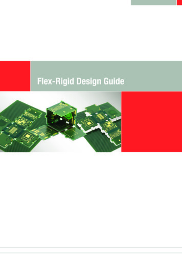
RIGID-FLEXPCB DESIGNA GUIDE BOOK FOR DESIGNERSBy Ben JordanEditors: Max Clemons, Ben Jordan
TABLE OF CONTENTSForeword3Introduction4Dynamic Flex Ideas25Flex-Circuit Materials5Static Flex Applications27Fab Considerations29Substrate and Coverlay Films5Conductors6Adhesives7Single Layer Flex Circuits7Flex & Rigid-Flex Fabrication Processes9Application Examples of Rigid Flex PCBsMulti-Layer Rigid-Flex2531How to maintain flexibility and lifespan withmultiple flex layers31Bookbinder Construction32Staggered Flexible Layer Bands33Flex build-ups9Getting Ultra-tight bends without sacrificing layer count 33Flex Fab Steps9Single Many-Layer Flex34Lamination and Routing12Flex Circuit Follies34Physical Constraints14Fab Documentation for Flex Circuits andRigid-Flex BoardsDocumentationDos and Don’ts of Flex Circuit DesignConclusion35Bibliography3616Additional Resources3720Glossary3816Do Keep Flex Flexible20Don’t Bend at Corners21Do Use Curved Traces21Don’t Abruptly Change Widths21Do Add Support for Pads22Allow for Squeeze-Out23Double-Sided Flex Routing23Do use Hatched Polygons23Via Placement24Defining Flex Cutouts and Corners24RIGID-FLEX CIRCUITS A GUIDE BOOK FOR DESIGNERSwww.altium.com
FOREWORDThe past year or two have been very challenging in the printed circuit board industry.Engineering managers, vice-presidents of operations and other functional managers areconstantly frustrated with sales and engineering trade-offs. Designers need tighter, higherdensity boards to keep up with customer demand.The printed circuit board is becoming more intricate in the overall product solution. This is becauseof pressure to do higher speed designs such as DDR3/4 and denser, lower power devices.Sierra has seen it’s fair share of these challenges, having focussed on quick-turn prototypesfor high-tech / HDI / and rigid-flex PCBs, and being a one-stop shop for helping electronicscompanies debug their prototypes through our fab, assembly, component procurementprocesses. This is no easy task.With this operational experience in mind, it is apparent that modern PCB design tools helpdesigners connect the dots efficiently, but for most packages there’s very little manufacturingknowledge built into the tool. This can make it hard to cleanly hand off the data forfabrication. So it’s very important for the designer to work closely with the fab to understandbuild strategy - ie. how it’s going to be built. Whatever the CAD tool used, there is still usuallya gap between what the designer creates and what is ready for manufacturing. Even withDesign Rule Checks, the fab usually has to call the designer or engineer to clarify issues thataffect manufacturability and yield.This industry needs to close the gap between the designer and the PCB production fab.Fortunately there is Altium. With a renewed focus on getting PCB design done right the firsttime, and willingness to be open and work with PCB fab and assembly shops like Sierra tomake sure that from the outset, we will have what we need to make the circuit to spec withoutcountless call backs.This Rigid-Flex guide book, and the new design capabilities within Altium Designer’s PCB Editor forRigid-Flex design, reflect a commitment to that openness.Amit BahlSierra ProtoexpressDecember 2013Sierra Protoexpresswww.protoexpress.comRIGID-FLEX CIRCUITS A GUIDE BOOK FOR DESIGNERSwww.altium.com3
INTRODUCTIONRigid-Flex can have many benefits, and many designers are at least considering it today whopreviously did not have to. More PCB designers are facing higher pressures to build evermore densely populated electronics, and with that comes additional pressure to reduce costsand time in manufacturing. Well, this is really nothing new of course. It’s just that the scopeof these pressures that the engineer and PCB designer have to respond to is continuouslybroadening. Rigid-Flex PCB technology offers a solution that is viable for many productdesigns facing these challenges.Yet there are aspects of rigid-flex technology which could be pot-holes in the road fornewcomers. So it’s wise to first understand how flex circuits and rigid-flex boards are actuallymade. From there we can look at the design issues imposed by the materials used, and thefabrication processes employed by most rigid-flex PCB manufacturers. And from there, wecan find a clear path to discover the best practices for rigid-flex PCB design.This guidebook is my attempt to clearly explain the materials, processes and design issuesin a way that will enlighten PCB designers of any level, who have not had a great deal ofexperience - if any - in designing of flex or rigid-flex circuits. It is based on a collectionof blog articles on the subject that were published on the AltiumLive blog pages athttp://blog.live.altium.com from August through October 2013. Though the blogs were a littlebit glib in places, we’ve done a reasonably good refactoring of the content to make sure it’snot missing anything essential - especially for those who have not yet done a rigid-flex PCBdesign.My hope is that this guidebook will form a good enough introduction to rigid-flex PCB designthat more readers will see the technology within reach for their own design projects, andthat a result overall will be increased adoption. And, with increased adoption there shouldbe decreased costs, which in turn will further increase access for more electronic productdevelopers to utilize rigid-flex boards.Let’s begin by looking at rigid-flex circuit materials.RIGID-FLEX CIRCUITS A GUIDE BOOK FOR DESIGNERSwww.altium.com4
CHAPTER 1FLEX-CIRCUIT MATERIALS1.1Substrate and Coverlay FilmsThe base material used in most common rigid printed circuit boards “The most common choice isis woven fibreglass impregnated in epoxy resin. It’s actually a fabric,polyimide, because it’s very flexible,and although we term these “rigid” if you take a single laminate layerthey have a reasonable amount of elasticity. It’s the cured epoxy which very tough, and also incredibly heatmakes the board more rigid. Because of the use of epoxy resins, they resistant.”are often referred to as organic rigid printed circuit boards. This is not flexible enoughfor many applications though for simple assemblies where there’s not going to beconstant movement it can be suitable.For the majority of flex circuit applications,more flexible plastic than the usual networkepoxy resin is needed. The most commonchoice is polyimide, because it’s very flexible,very tough (you can’t tear or noticeablystretch it by hand, making it tolerant ofproduct assembly processes), and alsoincredibly heat resistant. This makes it highlytolerant of multiple solder reflow cycles,Figure 1.1 Flexible Polyimide film. Shinmaxand reasonably stable in expansion andTechnology Ltd.contraction due to temperature fluctuations. For the majority of flex circuit applications,more flexible plastic than the usual network epoxy resin is needed.Polyester (PET) is another commonly used flex-circuit material,but it’s not tolerant enough of high temperatures to survivesoldering. I have seen this used in very low cost electronicswhere the flexible part had printed conductors (where the PETcould not handle the heat of lamination), and needless to saynothing was soldered to it - rather, contact was made by crudepressure with an Anisotropic conductive elastomer.Anisotropic Elastomers allowconduction vertically butnot horizontally.Anisotropic Elastomers allow conduction vertically but not horizontally.The display in the product in question (a clock radio) never really worked too well due tothe low quality of the flex circuit connection. So for rigid-flex we’ll assume we’re stickingto the PI film. (Other materials are available but not often used).RIGID-FLEX CIRCUITS A GUIDE BOOK FOR DESIGNERSwww.altium.com5
F le x - C irc u it M aterialsPI and PET films, as well as thin flexible-epoxy-and-glass-fibre cores, form commonsubstrates for flex circuits. The circuits must then use additional films (usually PI or PET,sometimes flexible solder mask ink) for coverlay. Coverlay insulates the outer surfaceconductors and protects from corrosion and damage, in the same way solder maskdoes on the rigid board. Thicknesses of PI and PET films range from 1/3 mil to 3 mils,with 1 or 2 mils being typical. Glass fibre and epoxy substrates are sensibly thicker,ranging from 2 mils to 4 mils.1.2ConductorsWhile the above-mentioned cheap electronics may use printed conductors - usually somekind of carbon film or silver based ink - copper is the most typical conductor of choice.Depending upon the application different forms of copper need to be considered. If youare simply using the flexible part of the circuit to reduce manufacturing time and costsby removing cabling and connectors, then the usual laminated copper foil (ElectroDeposited, or ED) for rigid board use is fine. This may also be used where heavier copperweights are desired to keep high-current carrying conductors to the minimum viablewidth, as in planar inductors.But copper is also infamous for work-hardening and fatigue. If your final applicationinvolves repeated creasing or movement of the flex circuit you need to consider highergrade Rolled Annealed (RA) foils. Obviously the added step of annealing the foil addsElectro-desposited CopperAnnealed CopperFigure 1.2 Exaggerated illustration of the annealing process, obviously not to scale. The copper foil passesbetween high-pressure rollers which elongate the grain structure in a planar orientation, making the coppermuch more flexible and springy in the normal.to the cost considerably. But the annealed copper is able to stretch more before fatiguecracking occurs, and is springier in the Z deflection direction - exactly what you wantfor a flex circuit that will be bending or rolling all the time. This is because the rollingannealing process elongates the grain structure in the planar direction.Examples of such an application would be gantry connections to a CNC router head, orlaser pickup for a Blu-Ray drive (Figure1.3).RIGID-FLEX CIRCUITS A GUIDE BOOK FOR DESIGNERSwww.altium.com6
F le x - C irc u it M aterialsFigure 1.3 Flex-circuit used to link the laser pickup to the main board assembly in a Blu-Ray mechanism.Notice that the PCB on the laser head has the flexible portion bent at right angles, and an adhesive beadhas been added for strengthening the flex circuit at the join(source: Zhuhai Smartech Electronics & Machinery).1.3AdhesivesTraditionally, adhesives are required for bonding the copper foil to PI (or other) films,because unlike a typical FR-4 rigid board, there’s less “tooth” in the annealed copper,and heat & pressure alone are not enough to form a reliable bond. Manufacturers suchas DuPont offer pre-laminated single- and double-sided copper clad films for flexiblecircuit etching, using acrylic or epoxy based adhesives with typical thicknesses of ½ and1 mil. The adhesives are specially developed for flexibility.“Adhesiveless” laminates are becoming more prevalent due to newer processes thatinvolve copper plating or deposition directly onto the PI film. These films are chosenwhen finer pitches and smaller vias are needed as in HDI circuits.Silicones, hot-melt glues, and epoxy resins are also used when protective beads areadded to the flex-to-rigid joins or interfaces (i.e. where the flexible part of the layerstack leaves the rigid part). These offer mechanical reinforcement to the fulcrum of theflex-to-rigid join which otherwise would rapidly fatigue and crack or tear in repeateduse. An example of this is shown in Figure 1.3 above.1.4Single Layer Flex CircuitsAn example of a typical single layer flex circuit cutaway view is illustrated inFigure 1.4. This is the same construction used for most common off-the-shelf FFC(Flexible Flat Connector) cables, which are an alternative to using rigid-flex PCBs wherethe FFC connectors can be accommodated and cost is the primary driving factor indesign decisions. In single-layer flex circuits the copper is pre-laminated on to the PIfilm by the material vendor, then etched and drilled with a rigid backing plate, andlaminated finally with adhesive-based PolyImide coverlay that is pre-punched to exposethe copper pads. The adhesives used in this arrangement for coverlay can squeeze outin the process, so it needs to be accommodated by enlarging the pads exposed areas.More will be discussed on this in Chapter 4.RIGID-FLEX CIRCUITS A GUIDE BOOK FOR DESIGNERSwww.altium.com7
F le x - C irc u it M aterialsIt’s important to be aware of the materials used in flexible and rigid-flex circuits. Eventhough you may generally allow the fabricator freedom to select the materials based onyour application, ignorance will not protect you from field-failures of the final product.A really good resource which contains far more detail than the brief introduction hereis Coombs, C. F. (Editor, 2008) The Printed Circuits Handbook, 6th Ed. 2008 McGrawHill, pp 61.3 0 - 61.24.CoverlayCoverlayAdhesiveBase AdhesiveEtched Copper TracesFigure 1.4Base PI FilmTypical single-layer Flex Circuit stack-upKnowing the material properties will also help in the mechanical design, evaluationand test of your product. If you are working on automotive products for instance; heat,moisture, chemicals, shock & vibe - all need to be modelled with accurate materialproperties to determine the product’s reliability, and minimum allowed bending radius.The irony is that the driving needs that cause you to choose flexible and rigid-flex areoften tied to harsh environments. For example, low-cost consumer personal electronicdevices are often subjected to vibrations, dropping, sweat and worse.RIGID-FLEX CIRCUITS A GUIDE BOOK FOR DESIGNERSwww.altium.com8
CHAPTER 2FLEX & RIGID-FLEXFABRICATION PROCESSES2.1Flex build-upsAt first glance, a t ypical flex, or rigid-flex board, looks “The fabricator may begin with prestraightforward. However the nature of these requires several laminated flex with foil, or may beginadditional steps in the build-up process. The beginning of anywith unclad Pl film and then laminaterigid flex board is always the single or double-sided flex layers.The fabricator may begin with pre-laminated flex with foil, or or plate up the copper for the initialmay begin with unclad PI film, and then laminate or plate up the cladding.”copper for the initial cladding. Laminating the film requires a thin layer of adhesive,whereas adhesiveless cladding requires a “seed” layer of copper. This seed layer isinitially planted using vapor deposition techniques (i.e. sputtering), and provides the keyto which chemically deposited copper is plated upon. This one or two-sided flex circuitis drilled, plated through, and etched in much the same steps as typical 2-sided coresin rigid boards.2.2Flex Fab StepsThe steps below show Flex-Circuit creation for a typical double-sided flex circuit.Adhesive/Seed coating appliedEither an epoxy or acrylic adhesive is applied, orsputtering is used to create a thin copper layer for aplating key.Copper foil addedCopper foil is added, either by lamination tothe adhesive (the more mainstream approach)or chemical plating onto the seed layer. Newerfabrication processes by materials vendors allowadhesiveless lamination of rolled annealed copper asan alternative.RIGID-FLEX CIRCUITS A GUIDE BOOK FOR DESIGNERSwww.altium.comAdhesive CoatingCopper Foil Lamnate9
F le x & R igid - F le x F abricati o n P r o cessesDrillingHoles to vias and pads are most often mechanicallydrilled. Multiple plated flex substrates can be drilledsimultaneously by combining them from multiplereels on drums, drilling between work plates, thenrolling out to separate reels on the other side of thedrilling machine. Pre-cut flex panels can be combinedand drilled between rigid blanks in the same wayrigid cores are drilled as well, though it requiresmore careful registration and the alignment accuracyis reduced. For ultra-small holes, laser drilling isavailable, though at much added cost because eachfilm has to be drilled separately. This would useExcimer (ultraviolet) or YAG (Infrared) lasers for higheraccuracy (microvias), and CO2 lasers for mediumholes (4 mils). Large holes and cutouts are punched,but this is a separate process step.Through-hole platingOnce the holes are made, copper is deposited andchemically plated in the same way as rigid PCB cores(commonly referred to as Cuposit). Through-holeplating in flex circuits is recommended to be at least1 mil in plating thickness to add mechanical supportto the pad or via, whereas a typical low-cost rigid PCBmay only have ½ mil cuposit.Drilling:(Mech. Laser or etch)Through-Hole PlatingEtch-resist printingPhotosensitive etch resist is coated onto the filmsurfaces, and the desired mask pattern is used toexpose and develop the resist prior to chemicaletching of the copper.Etch-ResistRIGID-FLEX CIRCUITS A GUIDE BOOK FOR DESIGNERSwww.altium.com10
F le x & R igid - F le x F abricati o n P r o cessesEtching and strippingAfter exposed copper is etched, the etch resist ischemically stripped from the flex circuit.Etching & StrippingCoverlay or CovercoatTop and bottom areas of the flex circuit are protectedby coverlay layers which are cut to shape. There maybe components actually mounted on sections ofthe flexible circuit, in which case the coverlay is alsoacting as a solder mask. The most common coverlaymaterial is additional polyimide film with adhesive,though adhesiveless processes are available. In theadhesiveless process, photoimageable solder mask(the same as used on rigid board sections) is used,essentially printing the coverlay onto the flex circuit.For coarser cheaper designs screen printing is alsoan option with final curing of this covercoat film byUV exposure. Basically, the difference is that coverlayis a laminated film, whereas covercoat is an appliedmaterial coating which then needs to be cured.Coverlay:Laminated or PrintedAlso, cutouts for component or connection pads in the coverlay leave at least two sidesof the pad land to anchor under it. You can see this clearly in Figure 2.1.Figure 2.1 An example of flex-circuit with Coverlay - notice that the openings in the coverlay are generallysmaller than the component pads (source: GC Aero Inc.).RIGID-FLEX CIRCUITS A GUIDE BOOK FOR DESIGNERSwww.altium.com11
F le x & R igid - F le x F abricati o n P r o cessesCutting out the flexThe final step in creating the flex circuit is cutting it out. This is often referred to as“blanking”. The high-volume cost-effective approach to blanking is by a hydraulic punchand die set (like the one shown in Figure 2.2), which involves reasonably high toolingcosts. However, this method allows punching out of many flex circuits at the sametime. For prototype and low-volume runs, a blanking knife is used. The blanking knife isbasically a long razor blade, bent into the shape of the flex circuit outline and affixed intoa routed slot in a backing board (MDF, plywood or thick plastic such as teflon). The flexcircuits are then pressed into the blanking knife to be cut out. For even smaller prototyperuns, X/Y cutters (similar to those used in vinyl sign making) could be used.Figure 2.22.3A blanking die for cutout of Flex Circuits (Source: Haoji Stamping Tool & Die Co.,Ltd.)Lamination and RoutingIf the flex circuit is to form a part of a rigid/flex combined stack-up (which is what we areinterested in), the process doesn’t stop there. We now have a flex circuit that needs to belaminated in between the rigid sections. This is the same as an individual drilled, platedand etched core layer pair, only much thinner and more flexible due to the lack of glassfibre. As noted previously though, a less flexible layer could be made with PI and glassdepending on the target application. Because this is being laminated in between rigidsections, it ultimately has to be framed in a panel that mates with the rigid board panelsections as well. Flex circuits that are not being combined with rigid sections are adheredtemporarily to a rigid backing board of MDF or FR-4 style materials.Laminated StackupsThe flex circuit is laminated into the panel along with the rigid and any other flexiblesections, with additional adhesive, heat and pressure. Multiple flex sections are notlaminated adjacent to each other unless you are designing multi-layer flex. This generallymeans each flex section has a maximum copper layer count of 2, so that flexibility ismaintained. These flex sections are separated by rigid pre-pregs and cores or PI bondingsheets with epoxy or acrylic adhesives.Essentially, each rigid panel is separately routed out in the areas where the flex is goingto be allowed to, well, flex.RIGID-FLEX CIRCUITS A GUIDE BOOK FOR DESIGNERSwww.altium.com12
F le x & R igid - F le x F abricati o n P r o cessesHere is an example process of laminating into a rigid-flex board, with two, 2-layer flexcircuits embedded between three rigid sections. The layer stack up would look like thatshown in Figures 2.3 & 2.4.Separate Cores, Pre-pregs, and Flexcircuits with ‘bikini’ coverlay, beforelamination in to the assembly panel.Drilled, plated and etchedcores, pre-pregs, and flexcircuit sections laminated intothe assembly panel.Final Rigid-Flex PCB. Normallycomponent assembly and reflowwould be done in the panel.Figure 2.3 How the Etched, plated, coverlayed and blanked flex panels are combined with the glass-epoxy rigid panels.Figure 2.4 Detailed Stack Diagram including plated-through holes for each flex section, as well as finalthrough-plated holes in the rigid section.In the example stack up shown in Figure 2.4, we have two pre-etched and cut flexcircuits, each double sided and plated through. The flex circuit has been blanked intoa final assembly panel including boarders for framing - this will keep the flex circuit flatduring final assembly after lamination with the rigid panel sections. There are certainlysome potential hazards with inadequate support of flex circuit elbows and large opensections during assembly - especially in the heat of a reflow oven.While this example does show adhesive layers it’s important to note that many designersare shying away from using adhesives, due to unacceptable z-axis expansion in reflow.However FR-4 prepreg and thermosetting epoxies effectively achieve the desiredresult and are for all intents and purposes here considered ‘adhesive’ layers. Additionaladhesion can be achieved through treatment of the copper on the flex layers to improvethe ‘tooth’ into the laminated prepregs. Adhesiveless double-sided flex laminates areshown here. These are entirely polyimide film with a bondable polyimide coating whichthe copper foil is bonded to. DuPont Pyralux and Rogers Corp. R/Flex are examplesof popular adhesiveless laminates.RIGID-FLEX CIRCUITS A GUIDE BOOK FOR DESIGNERSwww.altium.com13
F le x & R igid - F le x F abricati o n P r o cessesThe coverlay is also applied - like stickers laminated on with adhesive, or by a photoprinting process as mentioned earlier. Once the final flex and rigid panels in this 6-layerstackup are placed together, they are laminated with the outermost (top and bottom)final copper foil layers. Then another drilling for top-to-bottom plated through holes isdone. Optionally, laser drilled blind vias (top to first flex, bottom to last flex) could alsobe made, again adding expense to the design. The holes are plated through from topto bottom, and blind vias if there are any, and the final outer layer copper patterns areetched. The final steps are the printing of the top and bottom solder mask, top andbottom silkscreen and preservative plating (such as ENIG) or hot air leveling (HASL).Careful attention needs to be paid to layer pair planning and documentation for drillingand through-hole plating, because blind vias from a rigid surface layer down to anopposing flex-circuit layer will have to be back-drilled and add significant cost and loweryield to the fab process.2.4Physical ConstraintsMultiple Flex Sub-StacksWhile it’s possible to build just about any stack-up with rigid and flex sections, it canget ridiculously expensive if you’re not careful to consider the production steps and thematerial properties involved. One important aspect of flex circuits to remember is thestresses within the materials occurring as the circuit bends. Copper, being a non-ferrousmetal, is known to suffer work-hardening, and fatigue fractures will occur eventuallywith repeated flex cycling and tight radii. One way to mitigate this is to only use singlelayer flex circuits, in which case the copper resides at the center of the median bendradius and therefore the film substrate and coverlay are in the greatest compression andtension, as shown in Figure 2.5. Since the Polyimide is very elastic this is not a problem,and will last much longer under repeated movement than multiple copper layers will.Figure 2.5 For highly repetitive bending circuits, it’s best to use RA copper in single-layer flex to increasethe fatigue life (in cycles before failure) of the copper in the circuit.Along the same lines, having multiple separate flex circuits is often necessary, but it’sbest to avoid having bends at overlapping sections where the length of the flex sectionslimits the bend radius.Adhesive BeadsThere are times when you need to consider using strengtheners where the flex circuitexits the rigid board. Adding a bead of epoxy, acrylic or hot-melt will help improvethe longevity of the assembly. But dispensing these liquids and curing them can addRIGID-FLEX CIRCUITS A GUIDE BOOK FOR DESIGNERSwww.altium.com14
F le x & R igid - F le x F abricati o n P r o cesseslaborious steps to the production process, increasing cost. As always with PCB design,there are trade-offs.Automated fluid dispensing can be used, but you need to be really careful to collaboratewith the assembly engineers to make sure you don’t end up with globs of glue drippingunder the assembly. In some instances the glue must be applied by hand which addstime and cost. Either way, you need to provide clear documentation for the fabricationand assembly folks.Stiffeners & TerminationsExtreme ends of flex circuits typically terminate to a connector if not to the main rigidboard assembly. In these cases, the termination can have a stiffener applied (more thickPolyimide with adhesive, or FR-4). Generally then, it’s convenient to leave the ends ofthe flex embedded within the rigid-flex sections as well.The PanelThe rigid flex circuit stays together in it’s panel for the assembly process, so componentscan be placed and soldered on to the rigid terminations. Some products requirecomponents to be mounted also on flex in some areas, in which case the panel has tobe put together with additional rigid areas to support the flex during assembly. Theseareas are not adhered to the flex and are routed out with a controlled-depth router bit(with “mouse-bites”) and finally punched out by hand after assembly.Figure 2.6 Final Rigid-Flex panel example. Notice that this one has front and back board edges, and flexcircuit, routed out. The rigid sides are V-grooved for snapping off later. This will save time in assembly intothe enclosure (source: YYUXING Shenzhen Electronics Co., LTD.)RIGID-FLEX CIRCUITS A GUIDE BOOK FOR DESIGNERSwww.altium.com15
CHAPTER 3FAB DOCUMENTATION FOR FLEXCIRCUITS AND RIGID-FLEX BOARDS3.1DocumentationThis is essentially where we tell the fabricator what we want, andit’s probably the most likely part of the process where errors ormisunderstandings can make costly delays and waste happen.Fortunately there are standards we can reference to make sure weare communicating clearly to the fabricator, in particular IPC-2223.It could boil down to a few golden rules:“ODB v7.0 or later is preferred,since it has specific layer types addedto the job matrix that enable clearflex-circuit document for GenFlex and similar CAM tools.”1.Make sure your fabricator is capable of building your rigid-flex design.2.Make sure they collaborate with you on designing your layer stack to fit theirparticular processes.3.Use IPC-2223 as your point of reference for design, making sure the fabricatoruses the same & related IPC standards - so they are using the same terminologyas you.4.Involve them as early as possible in the process.Output Data SetIn interviewing a handful of rigid-flex capable board houses locally, we found that manydesigners still present gerber files to the board house. However ODB v7.0 or lateris preferred, since it has specific layer types added to the job matrix that enable clearflex-circuit documentation for GenFlex and similar CAM tools. Additionally ODB provides complete data sets for bare-board and in-circuit testing. A subset of the dataincluded is shown in table 1.Layer TypeBase TypeDescriptionCoverlaysolder maskClearances of a coverlay layerCovercoatsolder maskClearances of a covercoat layerPunchroutePattern for die-punching of the flex circuitStiffenermaskShapes and locations of stiffeners to be adheredBend AreamaskLabelling of areas that will be bent while in usePSAmaskPressure Sensitive Adhesive shapes andlocationsAreadocumentAn area definition (Rigid, Flex, or arbitrary)Table 1 Subset of Layer Types in ODB (v7.0 and later) used for GenFlex(Source: ODB v7.0 Specification)RIGID-FLEX CIRCUITS A GUIDE BOOK FOR DESIGNERSwww.altium.com16
F ab D o c u me n tati o n f o r F le x C irc u its a n d R igid - F le x B o ardsLayer TypeBase TypeDescriptionExposed AreadocumentAn exposed area of an inner layer and it’sassociated coverlay (could also be used forembedded components)Signal FlexsignalA signal layer for a flex circuitPower Ground pgFlexA power or ground layer for a flex circuitMixed FlexmixedMixed layer for a flex circuitPlating maskmaskA mask for defining which areas within a layershould be masked off from plating processImmersionMaskmaskA mask for defining which areas within a layershould be masked off for immersion goldTab
Dos and Don'ts of Flex Circuit Design 20 Do Keep Flex Flexible 20 Don't Bend at Corners 21 Do Use Curved Traces 21 Don't Abruptly Change Widths 21 . RIGID-FLEX CIRCUITS A GUIDE BOOK FOR DESIGNERS 4 www.altium.com INTRODUCTION Rigid-Flex can have many benefits, and many designers are at least considering it today who .
