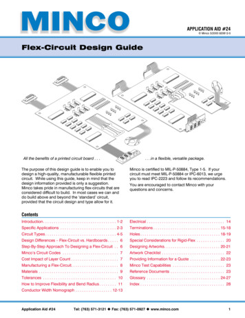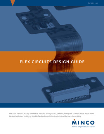
Transcription
FC302(A)F L E X C I R C U I TS DE S I G N G U I D EPrecision Flexible Circuitry for Medical Implants & Diagnostics, Defense, Aerospace & Other Critical ApplicationsDesign Guidelines for Highly Reliable Flexible Printed Circuits Optimized for Manufacturability
Minco Flex CircuitsTable of ContentsPurpose of this Design GuideIntroduction: Click below to view pagesThe purpose of this design guide is to enable you to design a highlyreliable, flexible printed circuit optimized for manufacturability.How to Get Started . . . . . . . . . . . . . . . . . . . . . . . . . . . . . . . . . . . . . 3Benefits of Flex Circuits . . . . . . . . . . . . . . . . . . . . . . . . . . . . . . . . . 4High reliabilitySuperior packaging solutionsDesign Options. . . . . . . . . . . . . . . . . . . . . . . . . . . . . . . . . . . . . . . . . 5Flex Circuit Design ProcessDesign Guidelines . . . . . . . . . . . . . . . . . . . . . . . . . . . . . . . . . . . 6 - 9Specification documentsManufacturing a flex circuitCost impact of layer countCircuit typesMinco's General Capabilities . . . . . . . . . . . . . . . . . . . . . . . 10 - 13Standard specificationsTestingMarkingControlling impedance and electrical noiseConductor width nomographStandard Design Recommendations . . . . . . . . . . . . . . . . . 14 - 19Design differences and special considerationsHow to improve flexibility and bend radiusHolesTolerancesConductor width, thickness and spacingMaterialsValue Added Design Options . . . . . . . . . . . . . . . . . . . . . . 20 - 23TerminationsStiffenersFormingPopulationCustom and Integrated ComponentsRequest a Quote . . . . . . . . . . . . . . . . . . . . . . . . . . . . . . . . . . 24 - 26Providing information for a quoteSpecify testing requirementsArtwork checklistDesigning artworksCAD data guidelinesE2E — Engineer to Engineer . . . . . . . . . . . . . . . . . . . . . . . . . . . 27Early engineering involvementOrdering and delivery . . . . . . . . . . . . . . . . . . . . . . . . . . . . . . . . . 27Place your order with MincoDelivery informationGlossary . . . . . . . . . . . . . . . . . . . . . . . . . . . . . . . . . . . . . . . . . . 28 - 30Next Steps . . . . . . . . . . . . . . . . . . . . . . . . . . . . . . . . . . . . . . . . . . . . 312While using this guide, keep in mind that the design informationprovided is only a suggestion. Minco takes pride in manufacturingflex circuits considered difficult to build. In most cases, we dobuild above and beyond the “standard” circuit specifications,provided that the circuit design and type allow for it.You are encouraged to contact Access: Minco Sales and Supportat 763.571.3121 with your questions and concerns.Types of Flex circuits Flex: Flexible version of Printed Circuit Board (PCB), withunique capabilities. Flex circuits offer the same advantages ofa printed circuit board: repeatability, reliability, and high density but with the added “twist” of flexibility and vibrationresistance. The most important attribute compelling designersto adopt flex circuit technology is the capability of the flex circuit to assume three-dimensional configurations. Rigid-flex: A blend of rigid and flex emphasizing the best ofboth constructions, adding synergistic capabilities neitherpossess. In its most typical configuration, the rigid-flex is as aseries of rigid PCBs joined by integrated flex circuits (withemphasis on the high percentage of rigid area content). Thereare many excellent possibilities for circuits designed primarilyas a flex circuit with the addition of integrated rigid areas.Rigid areas provide excellent hard mount points for components, connectors and chassis while flex areas offer dynamicflexing, flex to fit, and component mounting poised to takeadvantage of these low mass and vibration resistant zones.This blending leads to creative solutions for your mostdemanding applications. Flex-Coils : Custom wire-wound or etched coils may beintegrated with any of our flex circuit or rigid-flex board types.Whether bonded to the surface or encapsulated in a highdielectric and abrasion resistant covering, these assembliesoffer special capabilities to your coil designs.
How to Get Started1. Understand How Flex Circuits WorkCarefully review the information in this guide and otheronline resources at www.minco.com/flex/. Knowledge of flexcircuit types, capabilities and applications will provide theguidelines you need to design the best flex circuit for yourproduct.2. Build a Flex Circuit Mock-upThe dynamic nature of flex circuits allows for a multitude ofdesign options. The best method for determining the validityof your design is to create a physical flex circuit mock up. Tomake your mock-up, follow these steps:a. Determine the system points to be electrically connected via flex circuitry and termination method(s) such asmating connectors, pins, ZIF, etc.b. Determine approximate circuit “footprint” that will provide conductor routing to each termination location.c. Review schematic or net list details along with specialelectrical requirements, such as plane layers, to determine approximate layer count.d. Examine sample circuits of similar layer counts to determine if proposed design will provide sufficient flexibility(you can order a Flex Circuit Design Kit, which containscircuit and material samples, at www.minco.com).e. Review mechanical requirements to ensure that bendradii fall within acceptable values for circuit thickness andlayer count (refer to IPC-2223 for bend radius guidelines).f. Construct a “paper doll” outline of your flex circuit usingheavy paper and check for fit. Make modifications asnecessary. Continue constructing paper dolls and making modifications until the desired fit is achieved.g. Use .010" (0.25mm) polyester film to reconstruct thepaper doll to make a representative mock-up. Install andmake any dimensional adjustments as necessary.Your circuit outline is now complete and should be reconstructed in your CAD design software package. Using yourcircuit design software program, position connector footprints in the proper locations and route conductors perschematic or net list. Design rules for routing conductors onflexible circuits can be found in the IPC-2223 Sectional DesignStandard for Flexible Printed Boards. You can also refer to theStandard Design Recommendations section in this guide.3. Obtain a Mechanical SampleMinco will review your design for possible improvementsthen propose building a mechanical sample using actual circuit stack-up materials. Before investing a lot of time andmoney to create a functional flex circuit prototype, testing amechanical sample first ensures that your flex circuit has theright form and fit for your product. Form refers to the physical size, shape and mass of the part, while fit refers to itsenvironmental interfaces, e.g. is it flexible enough to bendfor installation, or will it meet temperature requirements? Amechanical sample helps you avoid installation problems orlatent mechanical issues that could cause failures.To receive a flex circuit mechanical sample proposal:a. Construct a simple 2-dimensional CAD model consistingof the circuit outline and hole locations and sizes.b. Convert the CAD model to a 2-D DXF format and includea text file that provides the layer count, any specialrequirements, and a brief explanation of your application. Also include your name, company name, postaland email address, and phone number.c. Email this information to sales@minco.com.d. Minco will provide a response with a lead time formechanical samples and advise if any charges arerequired.For More Information and CollaborationIf you would like application or design engineering assistance,call Access: Minco Sales and Support at 763.571.3121 or visit uson the web at www.minco.com. You can also collaborate withother design engineers faced with creating their own prototype. On the Minco “E2E” Engineer to Engineer DiscussionBoard, a special forum has been created specifically for designengineers.Share your prototyping experiences, ask questions or helpother design engineers looking for answers. Go to the E2ECommunity section on the Minco web site home page andclick on the “Discussion Forum”. Choose the “Interconnectivity”forum, or enter this link in your browser address line:www.minco.com/community/forums/3
Benefits of Flex CircuitsHigh reliabilitySuperior packaging optionsRepeatable installationCompared to discrete wiring, or ribbon cable, a flex circuit offersa customized repeatable routing path within your assembly. Thisgives you dependability where you need it. A flex circuit’slongevity can reduce service calls.Flex circuits can be shaped to fit where no other design can. Theyare a hybrid of ordinary printed circuit boards and round wire,exhibiting benefits of each. In essence, flex circuits give you unlimited freedom of packaging geometry while retaining the precisiondensity and repeatability of printed circuits.Flex vs. wiring harnessHarsh environmentsStandard practice for flex boards is to cover the conductors withpolyimide. This dielectric layer protects your circuits far beyondthe capability of simple soldermask. Other base and covermaterials are available for a broad range of ambient conditions.Long duty cyclesBy design, a flex circuit can be made very thin, yet robustenough to withstand thousands to millions of flexing cycleswhile carrying signal and power without a break.High vibrationUnder vibration and/or high acceleration, a flex circuit’s ductilityand low mass will reduce the impact upon itself and solderjoints. By contrast, a PCB’s higher vibrational mass will increasestresses upon itself, components and solder joints. Space and weight reduction: A single flex circuit can replace several hardboards, cables, and connectors. Fast assembly: Flex circuits eliminate the need to color code andwrap bundles of wire, reducing the chance of assembly rejectsand in-service failures. Total installed costs are lower, especiallywith volume production. Repeatable wire routing: Eliminate wire routing errors; reducingtest time, rework, and rejects Robust connections: Flat foil conductors dissipate heat better, carrying more current than round wires of the same cross-sectionalarea. Conductor patterns in a flex circuit maintain uniform electrical characteristics. Noise, crosstalk, and impedance can be predicted and controlled.Flex vs. hard board (PCB) Versatile shape: The most important attribute compelling designers adopt flex circuit technology is the capability of the flex circuitto assume three-dimensional configurations. Lower mass: With a little experimentation and imagination, a flexcircuit can save up to 75% of the space and/or weight of conventional wiring. Vibration resistance: Recurring costs are lower than many wireharnesses, and since a flex circuit is more resistant to shock andvibrations than a PCB, repair and replacement costs are less.Rigid-flexBefore: A tangle of wires connectsfour circuit boards.The flex circuit solution: A single circuitwith 7 stiffeners and 2 connectorsprovides all the needed interconnects. Double side component mounting: Rigid-flex are the idealsolution for flex circuits where surface mount components willbe mounted on both sides of the board. Total cost of ownership: The maximum benefit of rigid-flex isrealized when the complete installation is reviewed for totalcost of ownership. Using rigid-flex eliminates connections inthe flex-to-rigid transitions while improving impedance control. Most capable/Maximum vibration resistance: Lets you integratethe best capabilities of resistant rigid areas and resilient flex areas. High mass component mounting: When mounting a high masscomponent, a rigid board is the right solution. A rigid-flex boardgives you a smooth transition between rigid and flex areas whilepreserving the benefits of each.Flex-Coils Custom coil winding: State of the art equipment generates ahighly repeatable componentAfter: The package is neat, lightweight, and less susceptible to connectionfailure.4 Integrated assembly: allows best packaging of your fragile coil ina flex circuit sub-assembly.
Design OptionsRigid-flexPinsFine linesHybrid hardboard/flex circuits canhave up to sixteen layers. They replacebulky wire harnesses with compact,robust design.Minco can braze or solder pins tocircuits, either through holes or asextensions to conductors.0.002" conductors and spaces arepossible.StiffenersConnectorsShieldingAn inexpensive alternative to rigid-flex.Built-in connectors speed your assembly.Optional epoxy potting sealsbetween the circuit and connector.Solid or patterned shield planes reducenoise and control impedance of signallines. Use matched impedance flexcircuits for high-speed signal integrity.Wave solder carrierFactory formingCoilsStiffener material frames the circuit tohold it flat during wave solder. Aftersoldering, just clip out and install.Factory formed circuitsfollow tight curves to save space.Minco’s unique flat wound inductive coilscan be laminated into flex circuits.Applications include pacemaker antennasand eddy current generators.Surface mountSelective bondingIntegrated solutionsCombine the space and weight savingsof surface mounting with those of flexcircuits for the ultimate in high-densitypackaging.For better flexibility along circuit arms,individual layers are unbonded andallowed to flex freely. Each layer has it’sown substrate and cover.Minco integrates temperature sensors andetched-foil heaters with flex circuits forunified temperature control.5
Design GuidelinesSpecification documents:Consult standard specifications and design documents pertaining to your application and circuit requirements.IPC specifications*www.ipc.org IPC-2221A, Generic Standard on Printed Board Design IPC-2223, Sectional Design Standard for Flexible PrintedBoards IPC-4101, Specification for Base Materials for Rigid andMultilayer Printed Boards IPC-4202, Flexible Base Dielectrics for Use in Flexible PrintedCircuitry IPC-4203, Adhesive Coated Dielectric Films for Use as CoverSheets for Flexible Printed Circuitry and Flexible AdhesiveBonding Films IPC-4204 Flexible Metal-Clad Dielectrics for Use in Fabricationof Flexible Printed Circuitry IPC-6013, Qualification and Performance Specification forFlexible Printed Wiring IPC-MF-150, Copper Foil for Printed Wiring Applications IPC Position Paper: Transitioning from MIL-P-50884C andMIL-PRF-31032 to IPC-6013 and Amendment 1*For more information on IPC specifications, contact:IPC3000 Lakeside Drive, Suite 309 SBannockburn, IL 60015-1249 USATel: 847.615.7100 / FAX: 847.615.7105URL: http://www.ipc.org6Military www.dscc.dla.mil/Programs/MilSpec/DocSearch.asp MIL-P-50884 (inactive for new designs), Printed Wiring, Flexibleand Rigid-flex for Electronic Printed Wiring MIL-PRF-31032/3A, Printed Wiring Board, Flexible, Single andDouble Layer, With or Without Plated Holes, With or WithoutStiffeners, for Soldered Part Mounting MIL-PRF-31032/4A, Printed Wiring Board, Rigid-Flex or Flexible,Multilayer, with Plated Holes, with or Without Stiffeners, forSoldered Part MountingIPC recommends that companies using MIL-PRF-31032specifications for printed circuits, alternatively specify thatflexible circuits be supplied under IPC-6013 Class 3 performance requirements. Government agencies have generallyaccepted that this is a COTS (Commercial, Off-The-Shelf ) equivalent to MIL-PRF-31032. Please see the IPC position paperwhich is available for download at IPC.org or Minco.com.If your circuit must meet performance requirements ofMIL-P-50884, MIL-PRF-31032 or IPC-6013, we urge you to readthe IPC-2223 design specification for flexible circuits and followits recommendations.Minco documentswww.minco.com/flex/ Flex-Coils - Technical Specification FC01 Minco/Omnetics Flex Circuit Interconnect Solutions Technical Specification FC04 Designing for Flexibility and Reliability - Application AidFAA31
Design GuidelinesManufacturing a flex circuitBuilding a flex circuit generally involves the same steps from circuit to circuit. However, certain circuit designs can add cost. For example, a single-layer circuit with access holes on both sides is more expensive than a single-layer circuit with access on one side, becausethe double-sided access hole circuit must have its substrate drilled separately. The flow chart and illustrations below identify some costdriven issues, such as access holes, plated through-holes, etc. Theflow chart shows the manufacturing process for a r circuit with a erAdhesive1. Double-sided material is drilledTopCoverDrillBottomCoverDrill2. Through-holes are Access HolePad3. Copper is etched to createconductors and padsTackInspect4. Polyimide covers are laminatedover etched copperSolderDrillShipLaminateBlankCost impact of layer countIt is in your best interest to consider all options to minimizecost. For example, use two circuits to do the job of one. Twodouble-layer circuits may be less expensive than one four-layercircuit. But the cost savings of the circuit may be offset by additional assembly requirements. Circuits can also be folded inorder to save space and layers. Each situation is unique. A relatively small amount of time invested in project assessment canresult in significant savings overall.65COST MULTIPLIERThe information for the chart (right) was taken from a sample ofcircuits built with Minco’s standard materials. This chart is notintended to be used as a price guide. However, it does showthat circuit cost generally rises with layer 2-Layer3-Layer4-Layer4-LayerMulti-Layer Multi-Layer Rigid-FlexCIRCUIT TYPE7
Design GuidelinesCircuit typesSingle-layer IPC 6013, MIL-P-50884 - Type 1Access Hole One conductive layer, either bonded between two insulating layersor uncovered on one side.Cover**Adhesive* Access holes to conductors may be on either one or both sides.Access holes on both sides of a single-layer are more expensive sincethe substrate must be drilled or punched separately.Polyimide SubstrateCopper Pad Stiffeners, pins, connectors, components, are optional.Double-layer IPC 6013, MIL-P-50884 - Type 2 Two conductive layers with an insulating layer between; outer layersmay have covers or exposed pads.Access HolePolyimide CoverAdhesiveCopper Pad Plated through-holes provide connection between layers. Access holes or exposed pads without covers may be on either orboth sides; vias can be covered on both sides. Stiffeners, pins, connectors, components are optional.Polyimide CoverCopper-PlatedThrough-HolePolyimide SubstrateMultilayer IPC 6013, MIL-P-50884 - Type 3Access HoleCover Three or more flexible conductive layers with flexible insulating layersbetween each one; outer layers may have covers or exposed pads.Copper Pad Plated through-holes provide connection between layers.Polyimide SubstrateBond PlyPolyimide Substrate Access holes or exposed pads without covers may be on either orboth sides. Vias can be blind or buried. Stiffeners, pins, connectors, components are optional.AdhesiveCoverCopper-Plated Through-HoleMultilayer, not plated through-holes IPC 6013, MIL-P-50884 - Type 5Access Hole Two or more conductive layers with insulating layersbetween each one; outer layers may have covers or exposedpads.Cover**Adhesive* Through-holes are not plated.Cover** Access holes or exposed pads without covers may be oneither or both sides. Stiffeners, pins, and connectors are optional.Copper Pad (Layer #2)Copper Pad (Layer #1)Polyimide Substrate** Adhesiveless base material also available**Cover may be replaced by photo-imagable coverlay (PIC)8
Design GuidelinesCircuit typesRigid-flex IPC 6013, MIL-P-50884 - Type 4 Two or more conductive layers with either flexible or rigid insulationmaterial as insulators between each one; outer layers may havecovers or exposed pads. Rigid-flex has conductors on the rigid layers, whichdifferentiates it from multilayer circuits with stiffeners.AdhesivePlated through-holes extend through both rigid andflexible layers (with the exception of blind and buried vias).Rigid-flex costs more than a standard circuit with stiffeners.Rigid Material Access holes or exposed pads without covers may be oneither or both sides. Vias or interconnects can be fullycovered for maximum insulation.Polyimide CoverAdhesivePolyimide CoverPolyimide SubstratePolyimide SubstrateCopper PadCopper-Plated Through-Hole Stiffeners, pins, connectors, components, heat sinks, and mounting brackets are optional. We also manufacture “flush” rigid-flex, where the top surface of contact areas is levelwith adjacent adhesive/insulation. Minco is capable of sequentially laminating, drilling, and plating circuits, which allowsfor more flexibility in designing the circuit.Flex-Coils Coil-to-CircuitTerminationFlex-Coils are flex circuits containing integral wire coilsfor use as antennas or inductors. There are three basictypes of Flex-Coils: Simple, flat coils with wire leads Coils laminated inside flex circuits “Rim” coils that are built up in the Z-axisWire CoilEtched ConductorFlex-Coils have the same advantages that a flex circuit does. Wiring errors are reduced because the coil is oriented in the same spotevery time, which provides repeatable signals. Flex-Coils are rugged and easy to assemble, and their design usually guarantees areduced package size. A Flex-Coil can terminate in any manner that a flex circuit can, or to a wire lead. Heavy wire leads are available.See Flex-Coils Technical Specification FC01, for more information on Flex-Coil capabilities, design considerations, and the informationrequired for a quote or build.Integrated solutionsMinco is a leading manufacturer of temperature sensors andThermofoil flexible heaters. We have the unique ability to integratethese components and a flex circuit into a single package, drasticallyreducing assembly time and potential errors. Call Access: Minco Salesand Support to discuss your application, or visit www.minco.com.** Adhesiveless base material also available9
Minco’s General CapabilitiesStandard specificationsPhysical propertiesSurface finish (plating)Circuit size/standard panel size: 10.5 22" max./12 24",16.5 22" max./18 24", 267 x 559mm max./305 x 610mm,419 x 559mm max./457 x 610mmPlating methods: Panel, selective, thruhole, blind via, buried viaLayers: 16 maximum.Conductor width/space:0.0015” (0.038mm) minimum /0.0015” (0.038mm) minimum.Hole diameter (plated): 0.002” (0.051mm) minimum.Aspect ratio (ratio of hole depth/hole diameter):12:1 maximum.Outline dimensions and hole-to-border tolerance:SRD:0.015” (0.38mm) 0.1% linear distanceLaser/Hard tool: 0.003” (0.08mm) 0.1% linear distanceCMD:0.010” (0.25mm) 0.1% linear distanceCluster-to-cluster tolerance:0.002” (0.05mm) 0.1% linear distancePlating materials: Solder, hard gold, soft gold, tin, nickel, electroless nickel with immersion gold (ENIG), OSPElectrical characteristicsInsulation resistance: 100 MΩ minimum @ 25 C (77 F),assuming 0.010" (0.25mm) minimum conductor spacing.Dielectric (typical): 1000 VRMS @ 60 Hz for 30 seconds, 1 mAmaximum leakage current.Shield layers: Solid or grid patterns; copper foil or screenedconductive ink.Inductor/Antenna coils: Specify inductance (10 mH to 30 mH,typical). Wire-wound coils may be integrated into the circuit.The cover encapsulates the coil, conductors, and coil connections. For details, see Flex-Coils - Technical Specification FC01at www.minco.com/flex/.Bend radius (flexibility):Single-layer:6 circuit thickness (minimum)Double-layer:12 circuit thickness (minimum)Multilayer:24 circuit thickness (minimum)Circuit thickness is approximately 0.006" (0.15mm) per layer.Sharper, permanent bends are common for bend-to-installapplications. Call Access: Minco Sales and Support at763.571.3121 to ask about factory forming.Heaters/Temperature sensors: Minco is a leading manufacturer of temperature sensors and Thermofoil flexible heaters. Wehave the unique ability to integrate these components and aflex circuit into a single package, drastically reducing assemblytime and potential errors. Call Minco to discuss your application, or visit www.minco.com.Temperature: -65 to 150 C (-85 to 302 F).Will withstand a 5-second solder immersion at 260 C (500 F)without blistering, delaminating, or discoloring.Connectors:Clincher:0.100" (2.54mm) minimum, center-to-center;Micro series:0.050" (1.27mm) minimum, center-to-center;Nano series:0.025" (0.63mm) minimum, center-to-center.Optional epoxy potting is available.Chemical resistance: No detrimental loss of physical propertieswhen immersed for 15 minutes in acetone, methyl alcohol,toluene, or trichloroethylene.MaterialsCover/substrate: Polyimide film: 1 mil (25μm)*, 2 mil (50μm)*,3 mil (75μm), 5 mil (125μm); Photoimageable Coverlay (PIC);Epoxy glass or polyimide glass (rigid-flex)Conductor:Copper: 1/8 oz. (5μm), 1/4 oz. (9μm), 1/3 oz. (12μm),1/2 oz. (18μm)*, 1 oz. (35μm)*, 2 oz. (71μm), 3 oz. (107μm)Cupronickel: 0.625 mil (15μm), 0.9 mil (22μm), 1.3 mil (33μm),1.9 mil (48μm), 2.3 mil (58μm)Nickel: 2 mil (50μm), 5 mil (125μm)Adhesive: Acrylic*, flame retardant, epoxy, epoxy prepreg,polyimide prepreg, phenolicStiffener: Epoxy-glass (FR-4), polyimide-glass, polyimide, copper, aluminum.* These are the most common materials used for manufacturing flex circuitsfor maximum flexibility. See page 19 or contact Minco for materials not listed or special considerations (e.g. implantable devices, extended temperaturerange, etc.)10Value added assemblies**Fingers:Supported:0.006" (0.15mm) minimum, center-to-center;Unsupported:0.020" (0.50mm) minimum, center-to-center.In-line or right angle.Pins:Swaged/soldered: 0.085" (2.15mm) min., center-to-center;0.100" (2.54mm) typical;Brazed:0.035" (0.89mm) min., center-to-center.Active Components:Pick-and-place, Hand solder or brazeSurface mount, through hole, embedded** See pages 20 – 22 for more information on incorporating these assemblies into your design.Quality managementMinco is certified to ISO 9001: 2000 / AS/EN/SJAC9100quality system requirementsAll specifications subject to change.
Minco’s General CapabilitiesTestingMarkingWhen specifying testing, consider your needs carefully. Overspecification can greatly increase circuit cost. Minco encourageselectrical testing. It is required on all multilayer, rigid-flex, andfactory-formed circuits that are fabricated to MIL-P 50884, andcertain classes of IPC-6013.Minco can meet your marking requirements.See the table below for information on Minco’s test capabilities.Minco can test for Range of operationIPC-6013N.A.MIL-P-50884 conformanceComplete dimensionsResolution: 4 decimal placesAccuracy: 0.001” (0.025mm) 0.008% of linear distanceDielectric withstandingUp to 6000 VElectrical continuity1 Ω to 10 k Ω; suggest 5 ΩStimulus: 0.01 V to 5.0 VIonic cleanliness.5 microgram/square cmNACL equivalentInsulation resistance10 k Ω to 100 M Ω at 10 V to 250 VDCSuggest 100 M Ω at 100 VDCThermal shock-70 to 200 CMoisture resistanceUp to 98% relative humidityPlating thicknessDown to 0.000001" (0.02μm)Flexibility0 to 999,999 flexesMicrosectionsViewed at up to 1000 Our legend marking system offers silkscreen-like printing usinga durable white ink that meets IPC-TM-650 industry standards.This system allows us to incorporate date code and serial numbering, along with panel based marking, at the same time.We can also offer traditional epoxy ink hand stamp or silkscreenprinting if an alternate color or legacy specification is required.Etched marking within the part is also an option. Stiffeners andcovers may be marked with component mounting locations.Controlling impedance and electrical noisePredictable electrical characteristics make flex circuits an idealchoice for high-speed signal transmission. Uniform spacingbetween conductors and grounds, continuous shield layers,and repeatable geometries are features that help controlimpedance and reduce crosstalk. And with flex circuits, you caneliminate connectors and other transitions that contribute tosignal attenuation.Minco can provide tight tolerances on line width, spacing, anddistance to ground layers in order to meet your impedancerequirements. Actual impedance will also depend on the circuit’sshape after installation.Contact Minco for advice on designing circuits to specificelectrical characteristics. Microstrip - a single ground plane beneath the signal lines.SignalGround Stripline - dual ground layers above and below the signallines.GroundSignalGround Edge coupled differential pairs – traces are adjacent to eachother in the same plane with tightly controlled width andspacing, ground plane optional.SignalGround Rigid-flex/stiffened flex circuits with uninterrupted groundlayers. Silver epoxy coating. Silver epoxy is applied to the outside ofcircuits and electrically connected to other layers via accessholes in the cover coat. Silver epoxy shielding is more flexiblethan copper.11
Minco’s General CapabilitiesConductor width nomographThe nomograph on the facing page will help you determine themaximum allowable current capacity (in amperes) of a conductor. Reprinted from IPC-2221 (and MIL-STD-2118), the nomograph shows current for various conductor thicknesses, width,and temperature rises.Using the nomograph1. Locate the width of the conductor on the left side of thebottom chart.2. Move right horizontally, until you intersect the line of theappropriate conductor thickness. Move down vertically tothe bottom of the chart to determine the cross-sectional areaof the conductor.3. Move up vertically, until you intersect the line of the appropriate allowable temperature rise. This is the increase in temperature of the current-carrying conductor. Conductor temperature should not exceed 105 C. For example, if the ambient temperatur
guidelines you need to design the best flex circuit for your product. 2. Build a Flex Circuit Mock-up The dynamic nature of flex circuits allows for a multitude of design options. The best method for determining the validity of your design is to create a physical flex circuit mock up. To make your mock-up, follow these steps: a.