Transcription
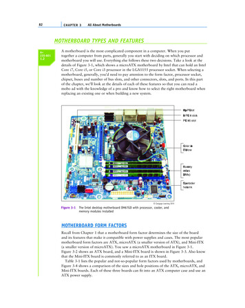
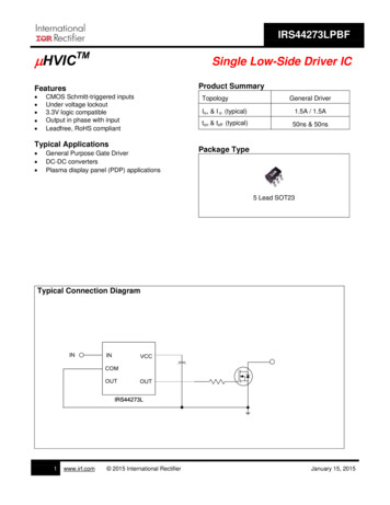
IRS44273LPBF HVICTMSingle Low-Side Driver ICProduct SummaryFeatures CMOS Schmitt-triggered inputsUnder voltage lockout3.3V logic compatibleOutput in phase with inputLeadfree, RoHS compliantTopologyTypical Applications General Purpose Gate DriverDC-DC convertersPlasma display panel (PDP) applicationsGeneral DriverIo & I o- (typical)1.5A / 1.5Aton & toff (typical)50ns & 50nsPackage Type5 Lead SOT23Typical Connection DiagramININVCCCOMOUTOUTIRS44273L1www.irf.com 2015 International RectifierJanuary 15, 2015
IRS44273LTable of ContentsPageTypical connection diagram1Description3Qualification Information4Absolute Maximum Ratings5Recommended Operating Conditions5Static Electrical Characteristics6Dynamic Electrical Characteristics6Functional Block Diagrams7Input/Output Pin Equivalent Circuit Diagram8Lead Definitions9Lead Assignments9Application Information and Additional Details10Package Details: SOT23-511Package Details: SOT23-5, Tape and Reel12Part Marking Information14Ordering Information152www.irf.com 2015 International RectifierJanuary 15, 2015
IRS44273LDescriptionThe IRS44273L is a low voltage, power MOSFET and IGBT non-inverting gate driver. Proprietary latch immuneCMOS technologies enable ruggedized monolithic construction. The logic input is compatible with standardCMOS or LSTTL output. The output driver features a current buffer stage.3www.irf.com 2015 International RectifierJanuary 15, 2015
IRS44273LQualification Information†Qualification LevelMoisture Sensitivity LevelMachine ModelESDHuman Body ModelIC Latch-Up TestRoHS s: This family of ICs has passed JEDEC’sIndustrial qualification. IR’s Consumer qualification level isgranted by extension of the higher Industrial level.MSL1††† 260 C(per IPC/JEDEC J-STD-020)Class B(per JEDEC standard JESD22-A115)Class 2(per EIA/JEDEC standard EIA/JESD22-A114)Class 1 Level A(per JESD78)YesQualification standards can be found at International Rectifier’s web site http://www.irf.com/Higher qualification ratings may be available should the user have such requirements. Please contact yourInternational Rectifier sales representative for further information.Higher MSL ratings may be available for the specific package types listed here. Please contact yourInternational Rectifier sales representative for further information.4www.irf.com 2015 International RectifierJanuary 15, 2015
IRS44273LAbsolute Maximum RatingsAbsolute maximum ratings indicate sustained limits beyond which damage to the device may occur. The devicemay not function or not be operable above the recommended operating conditions and stressing the parts tothese levels is not recommended. In addition, extended exposure to stresses above the recommended operatingconditions may affect device reliability. All voltage parameters are absolute voltages referenced to COM. Thethermal resistance and power dissipation ratings are measured under board mounted and still air conditions.DefinitionSymbolMinMaxVCCFixed supply voltage-0.325VOOutput voltage-0.3VCC 0.3Logic input voltagePackage power dissipation @ TA 25 CThermal resistance, junction to ambientJunction temperatureStorage temperatureLead temperature (soldering, 10 seconds)-0.3———-55—VCC 0.3250191150150300VINPDRthJATJTSTLUnitsVmW C/W CRecommended Operating ConditionsFor proper operation, the device should be used within the recommended conditions. All voltage parameters areabsolute voltages referenced to COM unless otherwise stated in the table. The offset rating is tested with supplyof VCC 15V.DefinitionSymbolVCCVOVINTAFixed supply voltageOutput voltageLogic input voltageAmbient temperature5www.irf.com 2015 International RectifierMinMax--00-4020VCCVCC125UnitsV CJanuary 15, 2015
IRS44273LStatic Electrical CharacteristicsVCC 15V, TA 25 C unless otherwise specified. The VIN, and IIN parameters are referenced to COM and areapplicable to input leads: IN. The VO and IO parameters are referenced to COM and are applicable to the outputleads: OUT.SymbolVCCUV VCCUVVCC UVHVILVIHVOHVOLIIN IINIQCCIO IO-DefinitionMin Typ Max UnitsVcc supply undervoltage positive going threshold 9.2 10.2 11.2Vcc supply undervoltage negative going threshold 8.2 9.2 10.2Vcc supply undervoltage lockout hysteresis— 1.0—Logic “0” input voltage (OUT LO)——0.8VLogic “1” input voltage (OUT HI)2.5——High level output voltage, VBIAS -VO——1.4Low level output voltage, VO—— 0.15Logic “1” input bias current—515µALogic “0” input bias current-30 -10—Quiescent VCC supply current— 170 340Output high short circuit pulsed current— 1.5—AOutput low short circuit pulsed current— 1.5—Test ConditionsIO 0 mAIO 20 mAVIN 5VVIN 0VVIN 0V or 5VVO 0V, VIN 5VVO 15V, VIN 0VDynamic Electrical CharacteristicsVCC 15V, TA 25 C, and CL 1000pF unless otherwise specified.Symboltontofftrtf6DefinitionTurn-on propagation delayTurn-off propagation delayTurn-on rise timeTurn-off fall timewww.irf.com 2015 International RectifierMin Typ Max Units—5095—5095ns—2555—2555Test ConditionsFigure 2January 15, 2015
IRS44273LFunctional Block om 2015 International RectifierJanuary 15, 2015
IRS44273LInput/Output Pin Equivalent Circuit RPDCOM8www.irf.comESDDiodeCOM 2015 International RectifierJanuary 15, 2015
IRS44273LPin te drive output4OUTGate drive output5VCCSupply VoltageLogic input for gate driver output (OUT)Pin Assignments1 INVCC 52 COM3 OUT9www.irf.com 2015 International RectifierOUT 4January 15, 2015
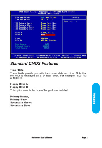
IRS44273LApplication Information and Additional DetailsINOUTFigure 1: Input/output Timing Diagram50%INton50%tofftr90%OUTtf90%10%10%Figure 2: Switching Time Waveform Definitions10www.irf.com 2015 International RectifierJanuary 15, 2015
IRS44273LPackage Details, SOT23-511www.irf.com 2015 International RectifierJanuary 15, 2015
IRS44273LPackage details: SOT23-5, Tape and Reel12www.irf.com 2015 International RectifierJanuary 15, 2015
IRS44273LPackage details: SOT23-5, Tape and Reel13www.irf.com 2015 International RectifierJanuary 15, 2015
IRS44273LPart Marking informationTop MarkingBOTTOM MARKING14www.irf.com 2015 International RectifierJanuary 15, 2015
IRS44273LOrdering InformationStandard PackBase Part NumberIRS44273LPackage TypeSOT23-5Complete Part NumberFormQuantityTape and Reel3000IRS44273LTRPBFThe information provided in this document is believed to be accurate and reliable. However, InternationalRectifier assumes no responsibility for the consequences of the use of this information. InternationalRectifier assumes no responsibility for any infringement of patents or of other rights of third parties whichmay result from the use of this information. No license is granted by implication or otherwise under anypatent or patent rights of International Rectifier. The specifications mentioned in this document are subjectto change without notice. This document supersedes and replaces all information previously supplied.For technical support, please contact IR’s Technical Assistance Centerhttp://www.irf.com/technical-info/WORLD HEADQUARTERS:101N Sepulveda Blvd., El Segundo, California 90245Tel: (310) 252-710515www.irf.com 2015 International RectifierJanuary 15, 2015
Features CMOS Schmitt-triggered inputs Under voltage lockout 3.3V logic compatible Output in phase with input Leadfree, RoHS compliant Typical Applications O General Purpose Gate Driver DC-DC converters Plasma display panel (PDP) applications 5 Lead SOT23 Product Summary C Topology General Driver I o & I o-