Transcription
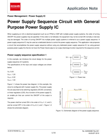
Application NotePower Management / Power Supply ICPower Supply Sequence Circuit with GeneralPurpose Power Supply ICWhen supplying an LSI or electrical equipment such as an FPGA or DSP with multiple power supply systems, the order of turningON/OFF the power supplies may be specified. If this order is not followed, the equipment may not be turned ON normally or devicesmay be damaged. The order of turning ON/OFF the multiple power supply systems is referred to as a power supply sequence. Apower supply sequence IC may be used as a dedicated device to control the power supply sequence. This application note proposesa circuit that accomplishes the power supply sequence without using any dedicated power supply sequence IC, by using generalpurpose power supply ICs that do not have the Power Good output or an output discharge function required for the sequence control.Power supply sequence specification 15VDCDC1VOUT11.2VDCDC2VOUT23.3VDCDC3VOUT31.5VIn this example, we introduce the circuit design for the powersupply sequence of 3 systems.The specifications of the input and output voltages are shownbelow.VIN: 5.0VVOUT1: 1.2VVOUT2: 3.3VFigure 1-1. Power treeVOUT3: 1.5VFigure 1-1 shows the power tree diagram. In this example, thecircuit is configured with 3 power supply ICs. The power supplyVOUT2: 3.3Vor linear regulators (LDO). As a function of the power supply IC,an enable pin that can control the ON/OFF of the output isrequired.The power shall be turned ON in the order of V OUT1, 2, and 3,and be turned OFF in the order of VOUT3, 2, and 1. Figure 1-2shows the schematic diagram.OUTPUT VOLTAGEICs are assumed to be switching regulators (DC/DC converters)VOUT3: 1.5VVOUT1: 1.2VtFigure 1-2. Schematic diagram of the power supply sequence 2019 ROHM Co., Ltd.1/16No. 62AN008E Rev.001AUGUST 2019
Power Supply Sequence Circuit with General Purpose Power Supply ICApplication NoteControl block diagram 1Figure 1-3 shows the control block diagram. DCDC 1, DCDC 2,Let’s follow the sequence operation in order. For the initial values,and DCDC 3 are the power supply ICs of 3 systems. Each outputthe Enable terminal is at the “Low” level and the outputs of the 3is controlled by the enable (EN) pin. Power Good 1 and 2 monitorDCDCs are zero. Figure 1-4 shows the operation in the first stepthe output voltage of the DCDCs when the power is turned ON,when the power is turned ON. First, the “High” voltage is appliedand output the “High” signal to the DCDC to be turned ON nextto the Enable terminal to turn ON the power supplies. The “High”when the output voltage reaches the target voltage. Power Goodvoltage is applied to the EN pin of DCDC 1 via diode D1 and3 and 4 monitor the output voltage of the DCDCs when theDCDC 1 is turned ON. When the output voltage of DCDC 1power is turned OFF, and output the “Low” signal to the DCDCincreases from 0 V to 1.2 V, the output voltage of Power Good 1to be turned OFF next when the output voltage reaches theswitches from “Low” to “High”. Then, the voltage is applied to thetarget voltage. The Discharge blocks ensure the normalEN pin of DCDC 2 on the next stage. In addition, since the “High”operation of the power supply sequence by rapidly dischargingvoltage is applied to the IN pins of Power Good 3 and Powerthe electric charges stored in the output capacitor of the DCDCsGood 4 via diodes D2 and D4, the PGOOD pins (output) areto decrease the voltage when the power is turned OFF. Note that,maintained at high impedance.in this block diagram, the logic is designed as Active Highbetween EN and VOUT of the DCDC blocks, between IN andPGOOD of the Power Good blocks, and between IN and OUT ofthe Discharge blocks. In addition, the PGOOD pin (output) of thePower Good blocks and the OUT pin of the Discharge blocks areof the open-collector or open-drain type.VIN5.0VEnableDCDC DCDC 15.0VVINRPULLUPL HHLINOUTDischarge 1LINOUTPower Good 1LPGOODINVOUT11.2VEND1Discharge 10V 1.2VVOUTPower Good 1LLHPGOODINLPower Good 3LPGOODINPGOODD3DCDC 2VINVOUTRPULLUPLPower Good 3D2L0VD3RPULLDOWNDCDC 2VINVOUTVOUT23.3VINLINOUTPower Good 2Power Good 2PGOODINLPGOODLPower Good 4LPGOODINLPGOOD0VVOUT31.5VRPULLUPDischarge 3INOUTVOUT31.5VDischarge 3INLOUTFigure 1-4. Operation when the power is turned ON: First stepFigure 1-3. Control block diagram 2019 ROHM Co., Ltd.0VRPULLDOWNEND6ENLD4IND5RPULLDOWNDCDC 3VINVOUTDCDC 3VINVOUTINPower Good 4D4D5D6VOUT23.3VDischarge 2OUTLLRPULLDOWNENDischarge 2RPULLUP0VRPULLUPENLD2IN2/16No. 62AN008E Rev.001AUGUST 2019
Power Supply Sequence Circuit with General Purpose Power Supply ICApplication NoteFigure 1-5 shows the operation in the second step when theFigure 1-6 shows the operation in the third step when the powerpower is turned ON. The “High” voltage is applied to the EN pinis turned ON. The “High” voltage is applied to the EN pin ofof DCDC 2 and DCDC 2 is turned ON. When the output voltageDCDC 3 and DCDC 3 is turned ON. The output voltage of DCDCof DCDC 2 increases from 0 V to 3.3 V, the output voltage of3 increases from 0 V to 1.5 V and all of the 3 power supplyPower Good 2 switches from “Low” to “High”. Then, the voltagesystems are now operating.is applied to the EN pin of DCDC 3 on the next stage.VIN5.0VEnableDCDC DCDC 15.0VVINRPULLUPHINPower Good 1PGOODPGOODINPGOODD3D3DCDC 2VINVOUT3.3VRPULLUPENRPULLDOWNVOUT23.3VENDischarge 2Discharge 2ININLOUTPower Good 2PGOODPGOODPGOODINRPULLUPPGOOD0VINPower Good 4D4IND5DCDC 3VINVOUTRPULLDOWND4IND5DCDC 3VINVOUTVOUT31.5VRPULLUPEND6Discharge 3INOUTPower Good 2HPower Good 4D6D2INRPULLDOWNVOUT20V 3.3V 3.3VRPULLUPINPower Good 3D2INDCDC 2VINVOUTHOUTPower Good 1PGOODLDischarge 1OUTPower Good 3VOUT11.2VEND1Discharge 1IN1.2VVOUTOUTLHVOUT30V 1.5V 1.5VENDischarge 3INFigure 1-5. Operation when the power is turned ON: SecondRPULLDOWNOUTFigure 1-6. Operation when the power is turned ON: Third stepstep 2019 ROHM Co., Ltd.3/16No. 62AN008E Rev.001AUGUST 2019
Power Supply Sequence Circuit with General Purpose Power Supply ICApplication NoteFigure 1-7 shows the state of the main nodes when the powerNext, we follow the sequence operation when the power issupplies are operating.turned OFF in order. Figure 1-8 shows the operation in the firststep when the power is turned OFF. First, the “Low” voltage isVIN5.0VEnableDCDC 15.0VVINRPULLUPHH1.2VVOUTapplied to the Enable terminal to turn OFF the power supplies.VOUT11.2VEND1The “Low” voltage is applied to the EN pin of DCDC 3 via diodeD6 and DCDC 3 is turned OFF. At the same time, the “Low”Discharge 1HINOUTvoltage is applied to the IN pin of Discharge 3 and the OUT pinHswitches to low impedance. This causes a rapid transition of thePower Good 1HPGOODINoutput voltage of DCDC 3 to 0 V. When the output voltage ofHDCDC 3 decreases, the output voltage of Power Good 4HPower Good 3HPGOODIND3DCDC 2VINVOUTRPULLUPHswitches from “High” to “Low”. Then, the voltage is applied to theD2H3.3VRPULLDOWNVOUT23.3VEN pin of DCDC 2 and the IN pin of Discharge 2 on the previousstage.ENDischarge 2HINOUTVIN5.0VHEnablePower Good 2HPGOODINDCDC 15.0VVINHLEND1Discharge 1INHHPGOODINHRPULLUPHPower Good 1PGOODRPULLDOWNINHDCDC 3VINVOUTHOUTD4D51.5VPower Good 3VOUT31.5VPGOODIND3DCDC 2VINVOUTDischarge 3HLD2HEND6INOUTVOUT11.2VRPULLUPHPower Good 41.2VVOUTHRPULLDOWNVOUT23.3V3.3VRPULLUPENFigure 1-7. State of main nodes when the power supplies areDischarge 2INoperatingOUTPower Good 2PGOODINHPower Good 4HLPGOODINLD4HD5DCDC 3VINVOUTHRPULLUPH LLLRPULLDOWNVOUT31.5V 0V 1.5VEND6Discharge 3HLINOUTHLFigure 1-8. Operation when the power is turned OFF: First step 2019 ROHM Co., Ltd.4/16No. 62AN008E Rev.001AUGUST 2019
Power Supply Sequence Circuit with General Purpose Power Supply ICApplication NoteFigure 1-9 shows the operation in the second step when theFigure 1-10 shows the operation in the third step when the powerpower is turned OFF. The “Low” voltage is applied to the EN pinis turned OFF. The “Low” voltage is applied to the EN pin ofof DCDC 2 and DCDC 2 is turned OFF. At the same time, theDCDC 1 and DCDC 1 is turned OFF. At the same time, the “Low”“Low” voltage is applied to the IN pin of Discharge 2 and the OUTvoltage is applied to the IN pin of Discharge 1 and the OUT pinpin switches to low impedance. This causes a rapid transition ofswitches to low impedance. This causes a rapid transition of thethe output voltage of DCDC 2 to 0 V. When the output voltage ofoutput voltage of DCDC 1 to 0 V. All of the 3 power supplyDCDC 2 decreases, the output voltage of Power Good 3systems are now turned OFF.switches from “High” to “Low”. Then, the voltage is applied to theEN pin of DCDC 1 and the IN pin of Discharge 1 on the previousstage.VIN5.0VEnableDCDC DCDC 15.0VVINRPULLUPLHLDischarge 1OUTINOUTPower Good 1PGOODVOUT11.2VEND1Discharge 1IN1.2V 0VVOUTPower Good 1INPGOODINLPower Good 3HLPGOODIND3DCDC 2VINVOUTPower Good 3D2H LPGOODRPULLDOWND3DCDC 2VINVOUTVOUT23.3V 0V 3.3VRPULLUPLRPULLDOWNVOUT23.3VENDischarge 2Discharge 2ININOUTOUTPower Good 2Power Good 2PGOODPGOODINPower Good 4PGOODRPULLUPPGOOD0VINPower Good 4D4IND5DCDC 3VINVOUTRPULLDOWND4IND5DCDC LDOWNVOUT31.5VEND6Discharge 3INOUTDischarge 3INOUTFigure 1-9. Operation when the power is turned OFF: SecondFigure 1-10. Operation when the power supply is turned OFF:stepThird step 2019 ROHM Co., Ltd.5/16No. 62AN008E Rev.001AUGUST 2019
Power Supply Sequence Circuit with General Purpose Power Supply ICVIN5.0VDCDC 1VINVOUTVOUT11.2VR147kEnableApplication NoteEN 10.01μR615k4DLYPGOOD GNDC30.01μR782IC1 BD4142HFVVCCINC2OP.D2 RB510SM-30IC2 BD4142HFVVCCINDLYPGOOD GNDR813kVPGOOD1 VOUT1 90% 1.2 0.9 1.08VVPGOOD3 0.5VC4OP.D3RB510SM-30R9100kDCDC 2R1047kVINVOUT23.3VVOUTEN 547k4DLYPGOOD GNDC70.01μR162.4kIC3 BD4142HFVVCCINC6OP.D4 RB510SM-30IC4 BD4142HFVVCCINDLYPGOOD GNDR1710kVPGOOD2 VOUT2 90% 3.3 0.9 2.97VVPGOOD4 0.5VC8OP.D5RB510SM-30R18100kDCDC 3R1947kVINVOUT31.5VVOUTEN k14Figure 1-11. Example of a circuit that accomplishes the power supply sequence 2019 ROHM Co., Ltd.6/16No. 62AN008E Rev.001AUGUST 2019
Power Supply Sequence Circuit with General Purpose Power Supply ICExample of circuit 1Application NoteSince the tolerance is 1.8% for the detection voltage ofBD4142HFV, the range of PGOOD is from 88.4% ( 90% Figure 1-11 shows an example of a circuit that accomplishes the0.982) to 91.6% ( 90% 1.018). In addition, since thepower supply sequence. The DCDCs in the 3 systems arehysteresis is 10 mV, the detection release voltage is 88.2% ( assumed to be switching regulators (DC/DC converters) or linear90% (0.5 V - 10 mV)/0.5 V) and the range is from 86.6% ( regulators (LDO). The DCDCs feature an enable (EN) pin that88.2% 0.982) to 89.8% ( 88.2% 1.018).can control the ON/OFF of the output.To delay the PGOOD flag, connect a capacitor to the DLY pin.The Power Good blocks use voltage detector IC BD4142HFV toThe delay time and the capacitance can be calculated withperform the Power Good function. Figure 1-12 features the mainEquation 1-2.part. This IC is equipped with a built-in hysteresis comparatorwith the detection voltage of 0.5 V. The detection voltage can beset using an external resistor. The detection voltage VPGOOD can𝐶2 𝑡𝐷𝐸𝐿𝐴𝑌[𝐹]2 106(1-2)be calculated with Equation 1-1.On the other hand, the PGOOD IC2 and IC4 operate when the𝑉𝑃𝐺𝑂𝑂𝐷𝑅2 𝑅3 0.5 [𝑉]𝑅3power is turned OFF. The detection is released (the output of the(1-1)PGOOD switches from “High” “Low”) when the output voltageof the DCDCs decreases to approximately 0.5 V or lower.In the example shown in Figure 1-11, VOUT1 is 1.2 V and thePGOOD of IC1 is set to output the flag when 90% of the outputThe Discharge block is configured with transistors and resistorsvoltage is reached. If the detection voltage is set to a higheras shown in Figure 1-13. The transistor in the first stage is avalue such as 95%, the PGOOD output switches to “Low” whensimple inverter circuit, and the transistor in the second stage isthe output voltage momentarily drops due to fluctuations in thea switch of an open-collector. The resistance connected in seriesload, disadvantageously causing momentary interruptions to theto the collector is varied to adjust the fall time of the outputDCDCs in the subsequent stages. The detection voltage shouldvoltage.be determined after understanding the specifications of thefluctuations in the load and the voltage drop. The detectionDCDC 1VINVOUTvoltage at 90% is 1.2 V 0.9 1.08 V. The resistor values canbe calculated from Equation 1 as follows.EN GND𝑉𝑃𝐺𝑂𝑂𝐷(15 𝑘𝛺 82 𝛺) 13 𝐾𝛺 0.5 V 1.08 [𝑉]13 𝑘𝛺5VR310k65Therefore, R2 is a series connection of 15kΩ and 82Ω and R3 ower GoodR147kR4100314VCCFigure 1-13. Discharge circuitUVLOHysteresis: 10mVINR24DELAY 0.5VR3The diodes at various locations are components for creatinglogic operations. Since the “Low” voltage needs to be maintained5DLY2GNDlow, Schottky barrier diodes with low forward voltages are used.C2Figure 1-12. Power Good function configured with BD4142HFV 2019 ROHM Co., Ltd.7/16No. 62AN008E Rev.001AUGUST 2019
Power Supply Sequence Circuit with General Purpose Power Supply ICApplication NoteExample of operation 1Figure 1-14 shows an example of the operation of the circuit inFigure 1-11. The voltage from the main power supply (VIN 5.0 V)is always applied. To turn ON the power, switch the Enable pinfrom “Low” to “High”. Then, the output is turned ON in the orderof VOUT1, 2, and 3 according to the specification initially created.Next, to turn OFF the power, switch the Enable pin from “High”to “Low”. The output is turned OFF in the order of V OUT3, 2, and1.Voltage [V]43Enable21065VIN 5.0VVIN 5.0VVOUT1 1.2VVOUT1 1.2VVoltage [V]4VOUT2 3.3VVOUT2 3.3VVOUT3 1.5VVOUT3 1.5V32100510Time [ms]1520Figure 1-14. Operation waveforms of the power supplysequenceIn this way, the power supply sequence can be accomplishedwithout using any dedicated power supply sequence IC, by usinggeneral purpose power supply ICs that do not have the PowerGood output or an output discharge function required for thesequence control. 2019 ROHM Co., Ltd.8/16No. 62AN008E Rev.001AUGUST 2019
Power Supply Sequence Circuit with General Purpose Power Supply ICApplication NotePower supply sequence specification 2In this example, we introduce the circuit design for the powersupply sequence of 3 systems.The specifications of the input and output voltages are shownbelow.VIN: 5.0VVOUT1: 1.2VVOUT2: 1.5VVOUT3: 3.3VFigure 2-1 shows the power supply tree diagram. In this example,the circuit is configured with 3 power supply ICs. The powersupply ICs are assumed to be switching regulators (DC/DCconverters) or linear regulators (LDO). As a function of the powersupply IC, an enable pin that can control the ON/OFF of theoutput is required.The power shall be turned ON in the order of V OUT1, 2, and 3,and be turned OFF in the order of VOUT1, 2, and 3 as well. Figure2-2 shows the schematic 3VFigure 2-1. Power treeOUTPUT VOLTAGEVOUT3: 3.3VVOUT2: 1.5VVOUT1: 1.2VtFigure 2-2. Schematic diagram of the power supply sequence 2019 ROHM Co., Ltd.9/16No. 62AN008E Rev.001AUGUST 2019
Power Supply Sequence Circuit with General Purpose Power Supply ICApplication NoteControl block diagram 2Figure 2-3 shows the control block diagram. DCDC 1, DCDC 2,Let’s follow the sequence operation in order. For the initial values,and DCDC 3 are the power supply ICs of 3 systems. Each outputthe Enable terminal is at the “Low” level and the outputs of the 3is controlled by the enable (EN) pin. Power Good 1 and 2 monitorDCDCs are zero. Figure 2-4 shows the operation in the first stepthe output voltage of the DCDCs when the power is turned ON,when the power is turned ON. First, the “High” voltage is appliedand output the “High” signal to the DCDC to be turned ON nextto the Enable terminal to turn ON the power supplies. The “High”when the output voltage reaches the target voltage. In addition,voltage is applied to the EN pin of DCDC 1 and DCDC 1 is turnedwhen turning the power OFF, the “LOW” signal is output to theON. When the output voltage of DCDC 1 increases from 0 V toDCDC to be turned OFF next when the target dropped voltage1.2 V, the output voltage of Power Good 1 switches from “Low”is reached. The Discharge blocks ensure the normal operationto “High”. Then, the voltage is applied to the EN pin of DCDC 2of the power supply sequence by rapidly discharging the electricon the next stage.charges stored in the output capacitor of the DCDCs to decreasethe voltage when the power is turned OFF. Note that, in this blockdiagram, the logic is designed as Active High between EN andVOUT of the DCDC blocks, between IN and PGOOD of thePower Good blocks, and between IN and OUT of the Dischargeblocks. In addition, the PGOOD pin (output) of the Power Goodblocks and the OUT pin of the Discharge blocks are of the opencollector or open-drain type.VIN5.0VEnableDCDC DC 15.0VVINHRPULLUPL HINDischarge 1OUTLINOUTPower Good 1LPGOODINPower Good 1LLLDCDC VPower Good 2LDCDC 3VINVOUTPGOOD0VDCDC 3VINVOUTVOUT33.3VRPULLUPENINENDischarge 3INOUTDischarge 3LFigure 2-3. Control block diagram 2019 ROHM Co., Ltd.0VOUTPower Good 2LVOUT21.5VDischarge 2OUTLL0VENDischarge 2RPULLUPINDCDC 2VINVOUTVOUT21.5VENLVOUT11.2VENDischarge 1L0V 1.2VVOUTINOUTFigure 2-4. Operation when the power is turned ON: First step10/16No. 62AN008E Rev.001AUGUST 2019
Power Supply Sequence Circuit with General Purpose Power Supply ICApplication NoteFigure 2-5 shows the operation in the second step when theFigure 2-6 shows the operation in the third step when the powerpower is turned ON. The “High” voltage is applied to the EN pinis turned ON. The “High” voltage is applied to the EN pin ofof DCDC 2 and DCDC 2 is turned ON. When the output voltageDCDC 3 and DCDC 3 is turned ON. The output voltage of DCDCof DCDC 2 increases from 0 V to 1.5 V, the output voltage of3 increases from 0 V to 3.3 V and all of the 3 power supplyPower Good 2 switches from “Low” to “High”. Then, the voltagesystems are now operating.is applied to the EN pin of DCDC 3 on the next stage.VIN5.0VEnableDCDC OUTRPULLUPDischarge 1INOUTOUTPower Good 1Power Good 1PGOODPGOODININDCDC 2VINVOUTVOUT20V 1.5V 1.5VVOUT11.2VENINRPULLUPHDCDC 15.0VDischarge 1DCDC 2VINVOUTLVIN5.0VRPULLUPEN1.5VVOUT21.5V0V 3.3VVOUT33.3VENDischarge 2Discharge 2ININLOUTOUTPower Good 2Power Good 2PGOODPGOODHDCDC 3VINVOUTRPULLUPIN0VDCDC 3VINVOUTVOUT33.3VRPULLUPENLHENDischarge 3Discharge 3ININOUTFigure 2-5. Operation when the power is turned ON: SecondINOUTFigure 2-6. Operation when the power is turned ON: Third stepstep 2019 ROHM Co., Ltd.11/16No. 62AN008E Rev.001AUGUST 2019
Power Supply Sequence Circuit with General Purpose Power Supply ICApplication NoteFigure 2-7 shows the state of the main nodes when the powerNext, we follow the sequence operation when the power issupplies are operating.turned OFF in order. Figure 2-8 shows the operation in the firststep when the power is turned OFF. First, the “Low” voltage isVIN5.0VEnableDCDC 15.0VHRPULLUPH1.2VVOUTVINapplied to the Enable terminal to turn OFF the power supplies.VOUT11.2V1 is turned OFF. At the same time, the “Low” voltage is appliedENDischarge 1HThe “Low” voltage is applied to the EN pin of DCDC 1 and DCDCINOUTto the IN pin of Discharge 1 and the OUT pin switches to lowHimpedance. This causes a rapid transition of the output voltagePower Good 1HPGOODINof DCDC 1 to 0 V. When the output voltage of DCDC 1Hdecreases, the output voltage of Power Good 1 switches fromDCDC 2VOUTVINRPULLUPH1.5VVOUT21.5V“High” to “Low”. Then, the voltage is applied to the EN pin ofDCDC 2 and the IN pin of Discharge 2 on the next stage.ENDischarge 2HINOUTHVIN5.0VPower Good 2HPGOODINHEnableHDCDC 15.0VVINLRPULLUPH L1.2V 0VVOUTVOUT11.2VENDischarge 1DCDC 3VOUTVINRPULLUPH3.3VINVOUT33.3VOUTPower Good 1ENHLPGOODDischarge 3HINOUTINHDCDC 2VINVOUTRPULLUPFigure 2-7. State of main nodes when the power supplies are1.5VVOUT21.5V3.3VVOUT33.3VENoperatingDischarge 2INOUTPower Good 2PGOODDCDC 3VINVOUTRPULLUPINENDischarge 3INOUTFigure 2-8. Operation when the power is turned OFF: First step 2019 ROHM Co., Ltd.12/16No. 62AN008E Rev.001AUGUST 2019
Power Supply Sequence Circuit with General Purpose Power Supply ICApplication NoteFigure 2-9 shows the operation in the second step when theFigure 2-10 shows the operation in the third step when the powerpower is turned OFF. The “Low” voltage is applied to the EN pinis turned OFF. The “Low” voltage is applied to the EN pin ofof DCDC 2 and DCDC 2 is turned OFF. At the same time, theDCDC 3 and DCDC 3 is turned OFF. At the same time, the “Low”“Low” voltage is applied to the IN pin of Discharge 2 and the OUTvoltage is applied to the IN pin of Discharge 3 and the OUT pinpin switches to low impedance. This causes a rapid transition ofswitches to low impedance. This causes a rapid transition of thethe output voltage of DCDC 2 to 0 V. When the output voltage ofoutput voltage of DCDC 3 to 0 V. All of the 3 power supplyDCDC 2 decreases, the output voltage of Power Good 2systems are now turned OFF.switches from “High” to “Low”. Then, the voltage is applied to theEN pin of DCDC 3 and the IN pin of Discharge 3 on the nextstage.VIN5.0VEnableDCDC PULLUPDischarge 1INOUTOUTPower Good 1Power Good 1PGOODPGOODININDCDC 2VINVOUTVOUT21.5V 0V 1.5VVOUT11.2VENINRPULLUPLDCDC 15.0VDischarge 1DCDC 2VINVOUTHVIN5.0V0VRPULLUPENVOUT21.5VENDischarge 2Discharge 2ININHOUTOUTPower Good 2Power Good 2PGOODPGOODLDCDC 3VINVOUTRPULLUPIN3.3VDCDC 3VINVOUTVOUT33.3VRPULLUPENHL3.3V 0VVOUT33.3VENDischarge 3Discharge 3ININOUTINOUTFigure 2-9. Operation when the power is turned OFF: SecondFigure 2-10. Operation when the power is turned OFF: Thirdstepstep 2019 ROHM Co., Ltd.13/16No. 62AN008E Rev.001AUGUST 2019
Power Supply Sequence Circuit with General Purpose Power Supply ICVIN5.0VDCDC 1VINVOUTVOUT11.2VR147kEnableApplication NoteEN GNDR410k65R2100kR5473Q1EMX12R3100k14C1 IC11μ BA8391G 5VCC1-IN4OUT IN 3VEE2 R922kR87.5kR647kVH VOUT1 90% 1.2 0.9 1.08VR79.1k VTH 0.79VVL 0.5VDCDC 2R1091kVINVOUT21.5VVOUTEN GNDR1310k65R11100kR14473Q2EMX12R12100k14C2 IC21μ BA8391G 5VCC1-IN4OUT IN 3VEE2 R1822kR179.1kR1547kR16 VH VOUT2 90% 1.5 0.9 1.35V11k VTH 0.925VVL 0.5VDCDC 3R1968kVINVOUT33.3VVOUTEN GNDR20100kR2210k65R23473Q3EMX12R21100k14Figure 2-11. Example of a circuit that accomplishes the power supply sequence 2019 ROHM Co., Ltd.14/16No. 62AN008E Rev.001AUGUST 2019
Power Supply Sequence Circuit with General Purpose Power Supply ICPGOODExample of circuit 2Figure 2-11 shows an example of a circuit that accomplishes thepower supply sequence. The DCDCs in the 3 systems areApplication NoteHLassumed to be switching regulators (DC/DC converters) or linearVL VTH VHregulators (LDO). The DCDCs feature an enable (EN) pin thatcan control the ON/OFF of the output.Figure 2-13. Hysteresis voltageThe Power Good block is configured with a non-invertinghysteresis comparator as shown in Figure 2-12, and theIn the circuit diagram shown in Figure 2-12, VTH is expressed bycomparator IC BA8391G is used for the device. A largeEquation 2-2. Converting this to the equation for R2 giveshysteresis voltage is provided between the detection voltageEquation 2-3.when turning ON the power (VH) and the detection voltage whenturning OFF the power (VL). This enables a single device todetect both voltages when turning the power ON and OFF to𝑉𝑇𝐻 output the control signals.𝑅2 VCCC11μFRPULLUP(2-2)𝑅1 𝑉𝑇𝐻[Ω]𝑉𝐶𝐶 𝑉𝑇𝐻(2-3)When R1 is 47kΩ and VCC is 5 V, R2 is 8.8kΩ according to the5BA8391Gfollowing equation. Select the nominal resistor value of 9.1kΩR1from the E24 series.VCC-IN 1PGOOD𝑅2 𝑉𝐶𝐶 [𝑉]𝑅1 𝑅2VTH4 OUTVEER2 IN 3𝑅2 2R447𝑘Ω 0.79𝑉 8.8𝑘Ω 9.1kΩ5𝑉 0.79𝑉R3VL, VHTo cancel the input bias current, select R3 so as to have thesame impedance as the inverting pin. The value is 7.6kΩFigure 2-12. Power Good function configured with a non-according to Equation 2-4, so select the nominal resistor valueinverting hysteresis comparatorof 7.5kΩ from the E24 series.First, we look at VH, the detection voltage when turning ON thepower. In the example shown in Figure 2-11, VOUT1 is 1.2 V and𝑅3 the PGOOD IC1 is set to output the flag when 90% of the output11 7.6𝑘Ω 7.5𝑘Ω1111 𝑅1 𝑅2 47𝑘Ω 9.1𝑘Ω(2-4)voltage is reached. The detection voltage VH is 1.2 V 0.9 1.08 V. Next, VL, which is the detection voltage when turningThe general calculations for obtaining VH and VL of a non-OFF the power, is set to 0.5 V. At this voltage, parasitic elementsinverting hysteresis comparator are described by Equations 2-5generally will not be turned ON even if reverse voltage is appliedand 2-6. Converting these to the equations for R4 and RPULLUPbetween the power supplies.gives Equations 2-7 and 2-8.The threshold voltage of the comparator (V TH) is set to themidpoint between VH and VL as shown in Figure 2-13. The value𝑉𝐻 (𝑅3 𝑅4 ) 𝑅2 𝑉𝐶𝐶 [𝑉]𝑅4 (𝑅1 𝑅2 )(2-5)𝑉𝐿 (𝑅3 𝑅4 𝑅𝑃𝑈𝐿𝐿𝑈𝑃 ) 𝑉𝑇𝐻 𝑅3 𝑉𝐶𝐶[𝑉]𝑅4 𝑅𝑃𝑈𝐿𝐿𝑈𝑃(2-6)𝑅4 𝑅2 𝑅3 𝑉𝐶𝐶[Ω](𝑅1 𝑅2 ) 𝑉𝐻 𝑅2 𝑉𝐶𝐶(2-7)can be calculated with Equation 2-1.𝑉𝑇𝐻 (𝑉𝐻 𝑉𝐿 ) 𝑉𝐿 [𝑉]2(1.08 0.5) 0.5 0.79 𝑉2 2019 ROHM Co., Ltd.(2-1)15/16No. 62AN008E Rev.001AUGUST 2019
Power Supply Sequence Circuit with General Purpose Power Supply IC𝑅𝑃𝑈𝐿𝐿𝑈𝑃 𝑅3 (𝑉𝑇𝐻 𝑉𝐶𝐶 ) 𝑅4 (𝑉𝑇𝐻 𝑉𝐿 )[𝑉]𝑉𝐿 𝑉𝑇𝐻Application NoteExample of operation 2(2-8)Figure 2-15 shows an example of the operation of the circuit inSubstitute the constants obtained above into Equations 2-7 and2-8 to determine the remaining values.Figure 2-11. The voltage from the main power supply (VIN 5.0 V)is always applied. To turn ON the power, switch the Enable pinfrom “Low” to “High”. Then, the output is turned ON in the orderof VOUT1, 2, and 3 according to the specification initially created.9.1𝑘Ω 7.5𝑘Ω 5𝑉𝑅4 (47𝑘Ω 9.1𝑘Ω) 1.08𝑉 9.1𝑘Ω 5𝑉Next, to turn OFF the power, switch the Enable pin from “High”to “Low”. The output is turned OFF in the order of VOUT1, 2, and(2-9)𝑅𝑃𝑈𝐿𝐿𝑈𝑃 3.47.5𝑘Ω (0.79𝑉 5𝑉) 22𝑘Ω (0.79𝑉 0.5𝑉)0.5𝑉 0.79𝑉(2-10) 86.9𝑘Ω 91kΩVoltage [V] 22.6𝑘Ω 22𝑘Ω3Enable210The Discharge block is configured with transistors and resistors6as shown in Figure 2-14. The transistor in the first stage is asimple inverter circuit, and the transistor in the second stage is5a switch of an open-collector. The resistance connected in seriesVIN 5.0VVIN 5.0Vto the collector is varied to adjust the fall time of the outputVOUT1 1.2VVOUT1 1.2V4Voltage [V]voltage.DCDC 1VINVOUTVOUT2 1.5VVOUT2 1.5VVOUT3 3.3VVOUT3 3.3V32EN GND1INR1100k5VR310k65R44730Q1EMX12R2100k01Figure 2-14. Discharge circuit510Time [ms]1520Figure 2-15. Operation waveforms of the power supply4sequenceIn this way, the power supply sequence can be accomplishedwithout using any dedicated power supply sequence IC, by usinggeneral purpose power supply ICs that do not have the PowerGood output or an output discharge function required for thesequence control. 2019 ROHM Co., Ltd.16/16No. 62AN008E Rev.001AUGUST 2019
NoticeNotes1) The information contained herein is subject to change without notice.2) Before you use our Products, please contact our sales representative and verify the latest specifications :3) Although ROHM is continuously working to improve product reliability and quality, semiconductors can break down and malfunction due to various factors.Therefore, in order to prevent personal injury or fire arising from failure, please take safetymeasures such as complying with the derating characteristics, implementing redundant andfire prevention designs, and utilizing backups and fail-safe procedures. ROHM shall have noresponsibility for any damages arising out of the use of our Poducts beyond the rating specified byROHM.4) Examples of application circuits, circuit constants and any other information contained herein areprovided only to illustrate the standard usage and operations of the Products. The peripheralconditions must be taken into account when designing circuits for mass production.5) The technical information specified herein is intended only to show the typical functions of andexamples of application circuits for the Products. ROHM does not grant you, explicitly or implicitly,any license to use or exercise intellectual property or other rights held by ROHM or any otherparties. ROHM shall have no responsibility whatsoever for any dispute arising out of the use ofsuch technical information.6) The Products specified in this document are not designed to be radiation tolerant.7) For use of our Products in applications requiring a high degree of reliability (as exemplifiedbelow), please contact and consult with a ROHM representative : transportation equipment (i.e.cars, ships, trains), primary communication equipment, traffic lights, fire/crime prevention, safetyequipment, medical systems, servers, solar cells, and power transmission systems.8) Do not use our Products in applications requiring extremely high reliability, such as aerospaceequipment, nuclear power control systems, and submarine repeaters.9) ROHM shall have no responsibility for any damages or injury arising from non-compliance withthe recommended usage conditions and specifications contained herein.10) ROHM has used reasonable care to ensurH the accuracy of the information contained in thisdocument. However, ROHM does not warrants that such information is error-free, and ROHMshall have no responsibility for any damages arising from any inaccuracy or misprint of suchinformation.11) Please
purpose power supply ICs that do not have the Power Good output or an output discharge function required for the sequence control. Power supply sequence specification 1 In this example, we introduce the circuit design for