Transcription
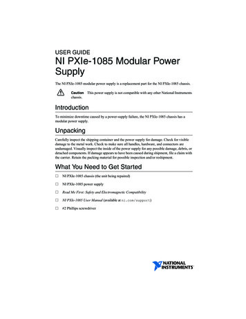
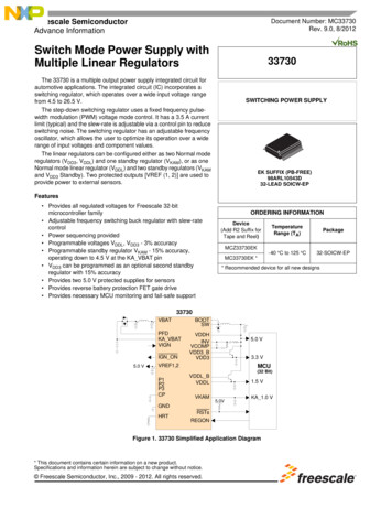
Freescale SemiconductorAdvance InformationDocument Number: MC33730Rev. 9.0, 8/2012Switch Mode Power Supply withMultiple Linear Regulators33730The 33730 is a multiple output power supply integrated circuit forautomotive applications. The integrated circuit (IC) incorporates aswitching regulator, which operates over a wide input voltage rangefrom 4.5 to 26.5 V.The step-down switching regulator uses a fixed frequency pulsewidth modulation (PWM) voltage mode control. It has a 3.5 A currentlimit (typical) and the slew-rate is adjustable via a control pin to reduceswitching noise. The switching regulator has an adjustable frequencyoscillator, which allows the user to optimize its operation over a widerange of input voltages and component values.The linear regulators can be configured either as two Normal moderegulators (VDD3, VDDL) and one standby regulator (VKAM), or as oneNormal mode linear regulator (VDDL) and two standby regulators (VKAMand VDD3 Standby). Two protected outputs [VREF (1, 2)] are used toprovide power to external sensors.SWITCHING POWER SUPPLYEK SUFFIX (PB-FREE)98ARL10543D32-LEAD SOICW-EPFeatures Provides all regulated voltages for Freescale 32-bitmicrocontroller family Adjustable frequency switching buck regulator with slew-ratecontrol Power sequencing provided Programmable voltages VDDL, VDD3 - 3% accuracy Programmable standby regulator VKAM - 15% accuracy,operating down to 4.5 V at the KA VBAT pin VDD3 can be programmed as an optional second standbyregulator with 15% accuracy Provides two 5.0 V protected supplies for sensors Provides reverse battery protection FET gate drive Provides necessary MCU monitoring and fail-safe supportORDERING INFORMATIONDevice(Add R2 Suffix forTape and Reel)TemperatureRange (TA)Package- 40 C to 125 C32-SOICW-EPMCZ33730EKMC33730EK ** Recommended device for all new designs33730 VBATPFDKA VBATVIGNIGN ON5.0 V BOOTSW VDDHINVVCOMPVDD3 BVDD35.0 V3.3 VVREF1,2MCU(32 Bit)P1P2P3CPVDDL BVDDLVKAM1.5 V5.0VKA 1.0 VGNDHRTRSTsREGONFigure 1. 33730 Simplified Application Diagram* This document contains certain information on a new product.Specifications and information herein are subject to change without notice. Freescale Semiconductor, Inc., 2009 - 2012. All rights reserved.
DEVICE VARIATIONSDEVICE VARIATIONSTable 1. Device VariationsPart no.Temperature RangeMCZ33730EKMC33730EKDescriptionReset detect circuitry- 40 C to 125 CImproved VDDL and VDD3 reset detect circuitry337302Analog Integrated Circuit Device DataFreescale Semiconductor
INTERNAL BLOCK DIAGRAMINTERNAL BLOCK orCPBuckKA VBATVKAMProtectionFETDriveHS DriveLevelShifterBOOTControl LogicVKAM15 mA, ILIM,TLIMSR –CPPFDFREQOscillator10.4 KChargePump –REG ON– INV1.98 KVBGVCOMPVIGNEnableIGN ONVDDHVDD3T-limVREF1VREF2StandbyControl5.0 VILIM 15 0mA26.5 V,-1V,TLIMBandgapPreference5.0 VP2P3Lim, TLimVDD3 BVDD3 SBYILim, TLimVDD3VBGVDDLIILIM 150 mALim26.5 V,-1V,TLIMP1IRef. VoltageProgrammingVDDL BVDDLVKAM, VDDL, VDD3,VDD3 SBYReference VoltageBlockRSTKAMVKAMReset DetectRSTHVDDHReset DetectRST3VDD3Reset DetectRSTLVDDLReset DetectHR TimerHRTGNDFigure 2. 33730 Simplified Internal Block Diagram33730Analog Integrated Circuit Device DataFreescale Semiconductor3
PIN CONNECTIONSPIN CONNECTIONSHRTRSTKAMRSTHRSTLRST3VREF2VDDLVDDHVDDL BVREF1REGONIGN 345678910111213141516P3VIGNGNDVDD3 BVDD3VKAMCPKA VBATVBATVBATSWSWSRBOOTPFDP2Note: The exposed pad is electrically and thermally connected to the IC ground.Figure 3. 33730 Pin ConnectionsTable 2. 33730 Pin DefinitionsA functional description of each pin can be found in the Functional Pin Description section beginning on page 12.Pin NumberPin NamePin FunctionFormal NameDefinition1HRTAnalogOutput2RSTKAMOpen DrainVKAM ResetThis pin is an open drain reset output, monitoring the VKAM supply to themicroprocessor.3RSTHOpen DrainVDDH ResetThis pin is an open drain reset output, monitoring the VDDH regulator.4RSTLOpen DrainVDDL ResetThis pin is an open drain reset output, monitoring the VDDL regulator.5RST3Open DrainVDD3 ResetThis pin is an open drain reset output, monitoring the VDD3 regulator.6VREF2Power OutputVREF Output 2This pin is the output of the protected supply VREF2. The pin is suppliedfrom the VDDH through the protection FET.7VDDLAnalog InputVDDL RegulatorThis pin is the VDDL regulator output feedback pin.8VDDHAnalog/Power InputVDDH RegulatorThis pin is the 5.0 V output feedback pin of the buck regulator. The pin isalso a power input for the protected outputs VREF1,2.9VDDL BAnalogOutputVDDL Regulator BaseDrive10VREF1Power OutputVREF Output 111REGONLogic InputRegulator Hold On12IGN ONOpen DrainVIGN Status13VCOMPAnalogOutputCompensationThis pin provides switching pre-regulator compensation, it is the output ofthe error amplifier.14INVAnalog InputInverting InputInverting input of the switching regulator error amplifier.15FREQHardware Reset Timer This pin is the hardware reset timer programmed with an external resistor.VDDL linear regulator base drive.This pin is the output of the protected supply VREF1. The pin is suppliedfrom the VDDH through the protection FET.Regulator Hold On input pin (5.0 V logic level input).This open drain output signals the status of the VIGN pin.Analog Input Frequency Adjustment Frequency adjustment of the switching regulator. The value of the resistorto ground at this pin determines the oscillator frequency.337304Analog Integrated Circuit Device DataFreescale Semiconductor
PIN CONNECTIONSTable 2. 33730 Pin Definitions(continued)A functional description of each pin can be found in the Functional Pin Description section beginning on page 12.Pin NumberPin FunctionFormal NameP1(1)Logic InputProgramming Pin 1Programming pin 1 for the VDD3, VDDL, and VKAM reference voltages.17P2(1)Logic InputProgramming Pin 2Programming pin 2 for the VDD3, VDDL, VKAM reference voltages.18PFDAnalogOutputProtection FET Drive19BOOTAnalog InputBootstrapThis pin is connected to the bootstrap capacitor.20SRAnalog InputSlew-rateSlew-rate Control of the switching regulator.21,22SWPower OutputSwitch Node23,24VBATPower InputBattery VoltageSupply25KA VBATPower InputKeep Alive Supply26CPAnalogOutputCharge Pump27VKAMPower OutputKeep Alive Memory28VDD3Analog Input VDD3 Linear Regulator16Pin NameDefinitionReverse battery protection FET gate drive.These pins are the source of the internal power switch (N-channelMOSFET).Voltage supply to the IC (external reverse battery protection needed insome applications).This pin is the keep alive supply input.External capacitor reservoir of the internal charge pump.Keep-Alive Memory (standby) supply output.This is a VDD3 regulator output feedback pin.This pin is also the output of the VDD3 standby regulator.This pin can be used also as an additional standby regulator without theexternal pass transistor.29VDD3 BAnalogOutputVDD3 LinearRegulator Base Drive30GNDGroundGround31VIGNAnalog InputVoltage IgnitionThis pin is the ignition switch control input pin. It contains an internalprotection diode.32P3(1)Logic InputProgramming Pin 3Programming pin 3 for the VDD3, VDDL, and VKAM reference voltages.This pin is a ground.Notes1. Programming pins must never be left floating, they must be tied to ground or protected battery voltage depending on the output voltageselections desired.33730Analog Integrated Circuit Device DataFreescale Semiconductor5
ELECTRICAL CHARACTERISTICSMAXIMUM RATINGSELECTRICAL CHARACTERISTICSMAXIMUM RATINGSTable 3. Maximum RatingsAll voltages are with respect to ground unless otherwise noted. Exceeding these ratings may cause a malfunction orpermanent damage to the device.RatingsSymbolValueUnitVBAT- 0.3 to 40VKA VBAT- 18 to 40V- 18 to 40VVBOOT- 0.3 to 50VVBOOT - VSW- 0.3 to 12VCharge Pump Output Voltage (CP)VCP- 0.3 to 12VSwitch Node Voltage SWVSW- 2.0 to 40VSensor Supplies (VREF1, VREF2)VREF- 1.0 to 26.5VVREFMAXSR2.0V/µsRegulator Voltages (VDDH,VDD3, VDD3 B, VDDL,VDDL B, VKAM)VREG- 0.3 to 7.0VOpen Drain Outputs (RSTH, RSTL, RST3, RSTKAM, IGN ON)VDD- 0.3 to 7.0VVREGON-0.3 to 7.0VVIN- 0.3 to 3.0VSupply Voltage (VBAT)Keep-Alive Supply Voltage (KA VBAT)Control Inputs (VIGN, P1, P2, P3), PFD OutputBootstrap Voltage (BOOT, SR) referenced to groundBootstrap Voltage (BOOT, SR) referenced to SWSensor Supplies (VREF1, VREF2) Maximum Slew RateRegon InputAnalog Inputs (VCOMP, INV, FREQ, HRT)ESDVoltage(2)VESDVHuman Body Model - HBM (all pins except BOOT, VDDL, RSTL) 2000Human Body Model - HBM (Pins BOOT, VDDL, RSTL) 1500Machine Model - MM (all pins) 200Charge Device Model - CDM (all pins) 750Operational Package Temperature (Ambient Temperature)Storage TemperaturePeak Package Reflow Temperature DuringMaximum Junction TemperatureThermal Resistance, Junction to AmbientThermal Resistance, Junction toCase(6)(5)Reflow(3), (4)TA MAX- 40 to 125 CTSTO- 65 to 150 CTPPRTNote 4 CTJ MAX150 CRθJ-A41 C/WRθJ-C1.2 C/WNotes2. ESD testing is performed in accordance with the Human Body Model (HBM) (AEC-Q100-2), the Machine Model (MM) (AEC-Q100-003),RZAP 0 Ω), and the Charge Device Model (CDM), Robotic (AEC-Q100-011).3.4.5.6.Pin soldering temperature limit is for 10 seconds maximum duration. Not designed for immersion soldering. Exceeding these limits maycause malfunction or permanent damage to the device.Freescale’s Package Reflow capability meets Pb-free requirements for JEDEC standard J-STD-020C. For Peak Package ReflowTemperature and Moisture Sensitivity Levels (MSL), Go to www.freescale.com, search by part number [e.g. remove prefixes/suffixesand enter the core ID to view all orderable parts. (i.e. MC33xxxD enter 33xxx), and review parametrics.Thermal resistance measured in accordance with EIA/JESD51-2.Theoretical thermal resistance from the die junction to the exposed pad.337306Analog Integrated Circuit Device DataFreescale Semiconductor
ELECTRICAL CHARACTERISTICSRECOMMENDED OPERATING CONDITIONSRECOMMENDED OPERATING CONDITIONSTable 4. Recommended Operating ConditionsAll voltages are with respect to ground unless otherwise noted.ParameterValueUnit*6.0 to 26.5VSwitching Regulator Output Current (IVDDH) total, VBAT 6.0 to 26.5 V0 to 2.0AVDD3 Standby Output Current0 to 15mAVKAM Standby Output Current0 to 15mAVREF1,2 Output Current0 to 100mA100 to 500kHzSupply Voltages (VBAT, KA VBAT)Switching Frequency Range* Tracks battery voltage from 6.0 down to 4.5 V.33730Analog Integrated Circuit Device DataFreescale Semiconductor7
ELECTRICAL CHARACTERISTICSSTATIC ELECTRICAL CHARACTERISTICSSTATIC ELECTRICAL CHARACTERISTICSTable 5. Static Electrical CharacteristicCharacteristics noted under conditions 6.0 V KA VBAT VBAT 26.5 V, - 40 C TA 125 C using the typical application circuit,unless otherwise noted.CharacteristicSymbolMinTypMaxUnitVKAM STUP4.5——VVSTUP4.5——VVSHDN R35—42VUVLO F3.6—4.3VUVLO R3.7—4.4VUVLO HYS—0.1———500GENERALKeep-Alive Start-up Voltage (at the KA VBAT pin), VKAM Output UpStart-up Voltage (at the KA VBAT pin), VDD3, VDD3 standby, VDDL UpOver-voltage ShutdownVVoltage at KA VBAT pin risingUnder-voltage Lock-outVVoltage at KA VBAT pin fallingVoltage at KA VBAT pin rising(7)Under-voltage Lock-out HysteresisSleep Quiescent Current (Sleep mode)IQVIGN 0 V, REGON 0 V, IVKAM 0 mA, VDD3 OFF, VBAT 14.0 V,µAKA VBAT 14 V (P1 1, P2 1, P3 1)SWITCHING REGULATOR (VDDH)Buck Converter Output VoltageVDDHVVBAT 6.0 to 26.5 V, ILOAD 100 mA4.95.05.1VBAT 26.5 to 35 V, ILOAD 100 mA4.855.05.15Switching Regulator Current Limit (see Figure 5)Pulse-by-Pulse Current LimitExtreme Current Limit (see Figure 5)(7)SW Drain Source OnResistance(7)AILIM SW-2.25-3.5-4.25ILIM SW SHYS1.0—20RDS(ON)ID 500 mA, VBAT 5.0 VThermal Shutdown Junction Temperature(7)Thermal Shutdown Hysteresis(7)mΩ C CVDD3 LINEAR REGULATORVDD3 Output Voltage (Includes Line and Load Regulation)VDD3IVDD3 0 to -500 mA, See Table 2 for VDD3 Output Settings%-3.0—3.0—1.11.5KA VBAT 14 V, VBAT 14 V-20—-50KA VBAT 5.0 V, VBAT 5.0 V-20—-50VDD3 Dropout Voltage (VDDH - VDD3)VDD3 DOIVDD3 -800 mA (VDD3 set to 3.3 V via P1, P2, P3 and with anexternal transistor)VDD3 B Current Limit, VDD3 B 0 V,VIVDD3B LimmANotes7. Guaranteed By Design.337308Analog Integrated Circuit Device DataFreescale Semiconductor
ELECTRICAL CHARACTERISTICSSTATIC ELECTRICAL CHARACTERISTICSTable 5. Static Electrical Characteristic(continued)Characteristics noted under conditions 6.0 V KA VBAT VBAT 26.5 V, - 40 C TA 125 C using the typical application circuit,unless otherwise .4UnitVDD3 STANDBY LINEAR REGULATORVDD3 Standby Output Voltage (Includes Line and Load Regulation)VDD3 SBYIVDD3 SBY 0 to -15 mA, See Table 2 for VDD3 SBY Output SettingVDD3 Dropout Voltage (KA VBAT - VDD3) Standby ModeVDD3 DO(VDD3 set at 3.3 V via P1, P2, P3) IVDD3 -10 mAVDD3 Standby Current Limit, VDD3 0 V%VIVDD3SBY LIMmAKA VBAT 14 V, VBAT 14 V-20—-50KA VBAT 5.0 V, VBAT 5.0 0—3.0——280KA VBAT 14 V, VBAT 14 V-18—-50KA VBAT 5.0 V, VBAT 5.0 V-18—-50-15—15Thermal Shutdown JunctionTemperature(8)Thermal Shutdown Hysteresis(8) C CVDDL LINEAR REGULATORVDDL Output Voltage (Includes Line and Load Regulation)VDDLIVDDL 0 to -500 mA, See Table 1 for VDDL Output SettingVDDL B Dropout Voltage (VDDH - VDDL)VDDL DO%mV(VDDL set at 3.3 V via P1, P2, P3) IVDDL -800 mAVDDL B Current Limit, VDDL 0 VIVDDL LIMmAVKAM STANDBY LINEAR REGULATORVKAM Output Voltage (Includes Line and Load Regulation)VKAMIVKAM 0 to -15 mA, See Table 1 for VKAM Output SettingVKAM Dropout Voltage (KA VBAT - VKAM)%VKAM DOIVKAM -10 mA, VKAM set to 5.0 V (P1 L, P2 H, P3 L)V——1.4VKAM STANDBY LINEAR REGULATOR (CONTINUED)VKAM Current Limit, VKAM 0 VIVKAM LIMmAKA VBAT 14 V, VBAT 14 V-20—-50KA VBAT 5.0 V, VBAT 5.0 rmal Shutdown Junction TemperatureThermal Shutdown Hysteresis(8)(8) C CNotes8. Guaranteed By Design.33730Analog Integrated Circuit Device DataFreescale Semiconductor9
ELECTRICAL CHARACTERISTICSSTATIC ELECTRICAL CHARACTERISTICSTable 5. Static Electrical Characteristic(continued)Characteristics noted under conditions 6.0 V KA VBAT VBAT 26.5 V, - 40 C TA 125 C using the typical application circuit,unless otherwise ��500mΩIREF LIM-150-280-450mAIREF REVLIM——40mAIREF REVLIM-2.0——mATSH——190 CTSL150——TSHYS5.0—20 CVIGN IH4.04.34.6VVIGN IL2.02.152.4VIGN-HYS1.7——SENSOR SUPPLIES VREF1, VREF2VREF On-resistance, IVREF -100 mAVREF Current Limit, VREF -1.0 V(9)VREF Reverse Current Limit, VREF 26.5 V(9)VREF Leakage Current, VREF Shut Down, VREF -1.0Thermal Shutdown Junction TemperatureV(9)(10)Thermal Shutdown Hysteresis(10)SUPERVISORY AND CONTROL CIRCUITSVIGN Input Voltage ThresholdVBAT 14.0 V, KA VBAT 14 VVIGN HysteresisVIGN Pull-down Current @ 5.0 VIPDVBAT 14.0 V, KA VBAT 14 VREGON Input Voltage ThresholdVµA103060VIH1.7——VBAT 14.0V, Battery Voltage 14VVIL-0.3—1.0REGON Input Voltage Threshold HysteresisVVIHYS0.10.30.4VREGON Pull-down Current @ 3.0 VIPD5.0—30µAProgramming Pin Input Voltage AVDDH Reset Upper Threshold Voltage (ΔVDDH/VDDH)4.08.013.0%VDDH Reset Lower Threshold Voltage (ΔVDDH/VDDH)-3.0-8.0-13.0%VDDL Reset Lower Threshold Voltage (ΔVDDL /VDDL)-3.0-8.0-13.0%VDD3 Reset Lower Threshold Voltage (ΔVDD3 0.4——0.4VBAT KA VBAT 14 VProgramming P1, P2, P3 Leakage Current @ 14.0 VVDD3 SBY Reset Lower Threshold Voltage(ΔVDD3 SBY /VDD3 SBY)VKAM Reset Lower Threshold Voltage (ΔVKAM /VkAM)%RSTH, RSTL, RST3, RSTKAM Low-level Output VoltageIOL 5.0 mAVIGN ON Low-level Output VoltageIOL 5.0 mA%VNotes9. The short circuit transient events on the VREF outputs must be limited to the voltage levels specified in the Maximum Ratings and slewrates of less than 2.0 V/µs, otherwise damage to the part may occur. Refer to the paragraph Sensor Supplies (VREF1, VREF2) on page18 and typical application circuit diagrams on Figure 8,and Figure 9 for recommended VREF output termination.10. Guaranteed by design.3373010Analog Integrated Circuit Device DataFreescale Semiconductor
ELECTRICAL CHARACTERISTICSDYNAMIC ELECTRICAL CHARACTERISTICSDYNAMIC ELECTRICAL CHARACTERISTICSTable 6. Dynamic Electrical CharacteristicsCharacteristics noted under conditions 6.0 V KA VBAT VBAT 26.5 V, - 40 C TA 125 C using the typical applicationcircuit, unless otherwise �12msGENERALPower On Reset Delay Time (HR Timer) (see Table 8)tD POR(Time to RESET up after Regulator in regulation)Power On Reset Delay Time (HR Timer) Accuracy (33 k resistor)ms(11)tLD P—500—µsOscillator Frequency (Switching Freq.) Range - Adjustable (Figure 4)Freq100—500kHzOscillator Frequency Tolerance at 100 kHz (FREQ Pin Open)fTOL90—110kHzProgramming Pin Latching DelaySWITCHING REGULATORSW Node Rise Time, VBAT KA VBAT 14 V, ISW 500mA(11)tSW RV/nsSR pin shorted to SW pin—0.96—SR pin open—1.82—SR pin shorted to BOOT pin—2.38—SR pin shorted to SW pin—0.83—SR pin open—0.83—SR pin shorted to BOOT pin—0.83—SW Node Fall Time, VBAT KA VBAT 14 V, ISW 500mA(11)tSW FV/nsNotes11. Guaranteed by design.33730Analog Integrated Circuit Device DataFreescale Semiconductor11
FUNCTIONAL DESCRIPTIONINTRODUCTIONFUNCTIONAL DESCRIPTIONINTRODUCTIONThe 33730 multi-output power supply integrated circuitaddresses the system power supply needs for applicationsusing the Freescale 32-bit microcontroller family architecture.FUNCTIONAL PIN DESCRIPTIONHARDWARE RESET TIMER (HRT)VDDL REGULATOR BASE DRIVE (VDDL B)This pin is the hardware reset timer input, which providesdelays for the Reset outputs. This delay is programmed by anexternal resistor to GND.VDDL linear regulator base drive. This output suppliescurrent into the base of the regulator external pass NPNtransistor.VKAM RESET (RSTKAM)VREF OUTPUT 1 (VREF1)This pin is an open drain reset output monitoring the VKAMsupply to the microprocessor. This output is actively pulledlow when the VKAM output voltage falls below its resetthreshold level.This pin is output of the protected supply VREF1. Thisoutput supplies sensors outside of the electronic controlmodule and therefore it is protected against short battery andshort to -1.0 V. This pin is supplied from the VDDH through theinternal protection FET.VDDH RESET (RSTH)This pin is an open drain reset output monitoring theVDDH regulator. This output is actively pulled low when theVDDH output voltage falls below its reset lower thresholdlevel or when the VDDH output voltage exceeds its resetupper threshold levelREGULATOR HOLD ON (REGON)Regulator Hold On input control pin. The 33730 can beenabled or kept in the Normal operational mode by holdingthis pin high. This is a 5.0 V logic input.VIGN STATUS (IGN ON)VDDL RESET (RSTL)This pin is an open drain reset output monitoring the VDDLregulator. This output is actively pulled low when the VDDLoutput voltage falls below its reset threshold level.This open drain output signals the status of the VIGN pin.This logic output is actively pulled low when the VIGN controlinput is pulled high.COMPENSATION (VCOMP)VDD3 RESET (RST3)This pin is an open drain reset output monitoring the VDD3regulator. This output is actively pulled low when the VDD3output voltage falls below its reset threshold level.This pin provides switching pre-regulator compensationnetwork. It is the output of the switching regulator erroramplifier.INVERTING INPUT (INV)VREF OUTPUT 2 (VREF2)This pin is output of the protected supply VREF2. Thisoutput supplies sensors outside of the electronic controlmodule and therefore it is protected against a battery shortand short to -1.0 V. This pin is supplied from the VDDHthrough the internal protection FET.VDDL REGULATOR (VDDL)This pin is the VDDL regulator output feedback pin. Theemitter of VDDL regulator external NPN pass transistor isconnected to this pin.VDDH REGULATOR (VDDH)This pin is the 5.0 V output feedback pin of the buckregulator. This pin is also a power input for the protectedoutputs VREF1 and VREF2.This pin is the inverting input of the switching regulatorerror amplifier.FREQUENCY ADJUSTMENT (FREQ)This is the frequency adjustment input of the switchingregulator. The operating frequency of the switching regulatorcan be programmed by an external resistor from this pin toground.PROGRAMMING PIN 1 (P1)Programming Pin 1 for the VDD3, VDDL, and VKAMreference voltage. The output voltage of the VDD3, VDDLand VKAM regulators can be programmed by the P1, P2, andP3 pins (see Table 7).3373012Analog Integrated Circuit Device DataFreescale Semiconductor
FUNCTIONAL DESCRIPTIONFUNCTIONAL PIN DESCRIPTIONPROGRAMMING PIN 2 (P2)KEEP ALIVE SUPPLY (KA VBAT)Programming Pin 2 for the VDD3, VDDL, and VKAMreference voltage. The output voltage of the VDD3, VDDLand VKAM regulators can be programmed by the P1, P2, andP3 pins (see Table 7).This pin is the keep alive supply input. This input is reversebattery protected. This input supplies power to the internalsupply and bias circuits that have to do with this VKAM andother always-on supplies.PROGRAMMING PIN 3 (P3)CHARGE PUMP (CP)Programming Pin 3 for the VDD3, VDDL, and VKAMreference voltages. The output voltage of the VDD3, VDDLand VKAM regulators can be programmed by the P1, P2, andP3 pins (see Table 7).External reservoir capacitor of the internal charge pump.This charge pump provides the voltage needed to sufficientlyenhance the gates of the internal n-channel mosfets (VREF1,VREF2, and VDDH) during the low battery condition.PROTECTION FET DRIVE (PFD)KEEP ALIVE MEMORY (VKAM)Reverse battery protection FET gate drive. This pin is anoutput drive for the gate of the external Reverse BatteryProtection N-channel FET.Keep Alive Memory (standby) supply output. This outputsupplies power for the module Keep-Alive memory. Thisoutput is always on, if the voltage at the KA VBAT pin isabove 4.5 V.BOOTSTRAP (BOOT)This pin is connected to the bootstrap capacitor. Itprovides the supply power for the switching regulator highside drive.SLEW-RATE (SR)Slew-rate Control of the switching regulator. The slew-rateof the switching regulator can be adjusted by connecting thispin to switch node (SW pin, slow slew-rate selection), BOOTpin (fast slew-rate selection), or it can be left open (mediumslew-rate selection).SWITCH NODE (SW)This pin is the source of the switching regulator internalpower switch (N-channel MOSFET source).VDD3 LINEAR REGULATOR (VDD3)This is a VDD3 regulator output feedback pin.The emitterof VDD3 regulator external NPN pass transitory is connectedto this pin.This pin can programmed to be the output of the VDD3Standby regulator (see Table 7).VDD3 LINEAR REGULATOR BASE DRIVE(VDD3 B)This pin can be used also as an additional standbyregulator without the external pass transistor.This outputsupplies current into the base of the regulator external passNPN transistor.GROUND (GND)BATTERY VOLTAGE SUPPLY (VBAT)Voltage supply to the IC (external reverse batteryprotection is recommended).This pin is the ground pin of the integrated circuit.VOLTAGE IGNITION (VIGN)This pin is the turn-on control input that is controlledthrough an ignition switch. This pin is reverse batteryprotected.33730Analog Integrated Circuit Device DataFreescale Semiconductor13
FUNCTIONAL DESCRIPTIONFUNCTIONAL INTERNAL BLOCK DESCRIPTIONFUNCTIONAL INTERNAL BLOCK DESCRIPTIONMC33730 - Functional Block DiagramOutput FunctionsInput FunctionsVoltage Programmming InputProtection FET Driver5 Volt Buck SwitchingRegulatorIgnition Input5 Volt Protected Outputs(VREF1, VREF2)Internal FunctionsLinear Regulator Outputs(VDDL, VDD3, VKAM)Band Gap ReferenceSleep/Wake CircuitryOscillator5.0 VOLT BUCK REGULATORThis is the main regulator that supplies 5.0 Volts to thefollowing protected and regulated outputs, VREF1, VREF2,VDD3, and VDDL.OSCILLATORThis is the frequency source for the switching (buck) 5 Voltregulator. The frequency of oscillation is selected by anexternal resistor to ground.BAND GAP REFERENCEThis is the main voltage reference, which is used as thestandard for all the current and voltage sources in theMC33730.PROTECTION FET DRIVERThe protection FET is used to prevent reverse batteryconnections from damaging the MC33730. The gate drive forthe Protection FET is provided by this driver circuit.Ignition DriverReset Circuitryoutput signal to indicate that the ignition switch has beenactivated.VREF1This output is one of two protected 5.0 volt outputs that canbe used to supply external sensors or other analog circuitsrequiring a regulated, short-circuit protected 5.0 volt supply.VREF2This output is one of two protected 5.0 volt outputs that canbe used to supply external sensors or other analog circuitsrequiring a regulated, short-circuit protected 5.0 volt supply.VDD3 REGULATORThis is one of three, voltage programmable, regulatedsupplies. This supply is controlled by the ignition switch.VDDL REGULATORThis is one of three, voltage programmable, regulatedsupplies. This supply is controlled by the ignition switch.SLEEP/WAKE CIRCUITRYThis circuitry is responsible for the two main modes ofoperation for the MC33730, Sleep mode and Wake mode. Inthe Sleep mode, only the keep alive outputs are active, andthe rest of the circuitry is in a low power drawing sleep state.In the Wake mode, the MC33730 is fully functional andnormal current is being consumed.IGNITION DRIVERThis block of circuitry controls all the voltage outputs,except for the keep alive voltage output(s). It also provides anVKAMThis is one of three, voltage programmable, regulatedsupplies. This supply is NOT controlled by the ignition switch.VOLTAGE PROGRAMMINGP1, P2, and P3 are three logic level inputs that control thevoltage that is available on the VDD3, VDDL and VKAMoutputs.Table 7 indicates the 8 different combinations of P1, P2,and P3 and the resultant voltage values.3373014Analog Integrated Circuit Device DataFreescale Semiconductor
FUNCTIONAL DESCRIPTIONFUNCTIONAL INTERNAL BLOCK DESCRIPTIONRESET CIRCUITRYREGON INPUTThere are four open drain reset lines that indicate thestatus of the four voltage outputs; VDDH, VDDL, VDD3, andVKAM. They are labeled: RSTH, RSTL, RST3, andRSTKAM.This input is OR’d with VIGN. However, it is a 5.0 volt logicinput, as opposed to VIGN, which is a VBAT level input. Thisinput is controlled by an MCU I/O pin, to hold power up whenthe ignition switch is turned off, so housekeeping functionscan be performed before power is shut off, by lowering theREGON line. IF REGON is not needed, it should be tied toGND.33730Analog Integrated Circuit Device DataFreescale Semiconductor15
FUNCTIONAL DEVICE OPERATIONOPERATION DESCRIPTIONFUNCTIONAL DEVICE OPERATIONOPERATION DESCRIPTIONThe 33730 has two supply inputs. The KA VBAT pin is thesupply input for the standby regulators VKAM (and optionallyVDD3 SBY, see Table 7) and for the internal supply circuits.The VBAT pin is the power input of the integrated buckregulator, which steps-down the protected battery voltageproviding directly the 5.0 V system supply VDDH. VDDHprovides power for the main linear regulator(s) VDDL, VDD3,and also for the other module circuits requiring 5.0 V supplyvoltage (e.g. protected VREF1,2 outputs).If the supply voltage ramps from zero volts up to itsnominal level, the 33730 will start at the latest when thesupply (battery) voltage reaches VSTUP at the KA VBAT pin.If the supply voltage ramps down, the 33730 will keepoperating (with degradation of the output voltage regulation)down to VUVLO f at the KA VBAT pin. The VKAM output staysoperational down to VUVLO f at the KA VBAT pin.The 33730 will operate in systems with and withoutstandby mode. In the Standby (sleep) mode of operation theIC will draw maximum IQ quiescent current, assuming onlythe VKAM is used as a standby output, and it is unloaded.When VDD3 is used as an additional standby output thequiescent current increases by approximately another100 μA.POWER UPThe 33730 will safely power up when the power is appliedsimultaneously (hot plugged) or in the random sequence tothe KA VBAT, VBAT and VIGN (or REGON) inputs.POWER DOWNThe 33730 will safely power down when the power isdisconnected from any of the KA VBAT, VBAT inputs orwhen control signals the VIGN or REGON inputs go low.UNDERVOLTAGE LOCK-OUT (UVLO)There is an under-voltage lock-out feature implementedinto the IC. When the battery voltage at the KA VBAT pinfalls below VUVLO f the under-voltage comparator initiates thepower down sequence for the whole IC. The under-voltagelock-out circuit has a VUVLO hys hysteresis and 5.0 μs glitchfilter in order to prevent spurious tripping its threshold leveland consequent system oscillations between the ON andOFF states.SWITCHING REGULATORThe 33730 switching regulator is a fixed frequency(externally adjustable) PWM voltage mode controller withintegrated low-RDS(ON) N-channel power MOSFET. Thisarchitecture is widely flexible and provides a possibility tooptimize its operation over a wide range of input voltages.The 33730 switching regulator provide the following features:Adjustable Switching FrequencyThe adjustable frequency feature provides the ability tomodify the switcher performance for optimized cost (higherfrequency, smaller, cheaper components), or higherefficiency and better EMC performance (lower switchingfrequency for reduced losses and EMI). The operatingfrequency of the switching regulator can be adjusted bymeans of an external resistor RF connected from the FREQpin to ground (see Figure 4).Frequency vs RFreq600Switching Frequency [kHz]INTRODUCTION5004003002001000020406080100RFreq [kohm ]FSW 18.48 (5098.7/RFREQ)FSW is the switch frequency in kHzRFREQ is the resistor value in kOhmsFigure 4. Switching Regulator Frequency vs. RFreq ValueAdjustable Slew-rateThe adjustable slew-rate option allows, with selection ofthe right s
Switch Mode Power Supply with Multiple Linear Regulators The 33730 is a multiple output power supply integrated circuit for automotive applications. The integrated circuit (IC) incorporates a switching regulator, which operates over a wide input voltage range from 4.5 to 26.5 V. The st