Transcription
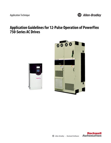
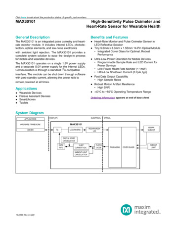
Click here to ask about the production status of specific part numbers.MAX30101High-Sensitivity Pulse Oximeter andHeart-Rate Sensor for Wearable HealthGeneral DescriptionBenefits and FeaturesThe MAX30101 is an integrated pulse oximetry and heartrate monitor module. It includes internal LEDs, photodetectors, optical elements, and low-noise electronics Heart-Rate Monitor and Pulse Oximeter Sensor inLED Reflective Solution Tiny 5.6mm x 3.3mm x 1.55mm 14-Pin Optical Module Integrated Cover Glass for Optimal, RobustPerformancewith ambient light rejection. The MAX30101 provides acomplete system solution to ease the design-in processfor mobile and wearable devices.The MAX30101 operates on a single 1.8V power supplyand a separate 5.0V power supply for the internal LEDs.Communication is through a standard I2C-compatibleinterface. The module can be shut down through softwarewith zero standby current, allowing the power rails toremain powered at all times. Fast Data Output Capability High Sample Rates Robust Motion Artifact Resilience High SNRApplications Ultra-Low-Power Operation for Mobile Devices Programmable Sample Rate and LED Current forPower Savings Low-Power Heart-Rate Monitor ( 1mW) Ultra-Low Shutdown Current (0.7μA, typ) -40 C to 85 C Operating Temperature RangeWearable DevicesFitness Assistant DevicesSmartphonesTabletsOrdering Information appears at end of data sheet.System DiagramAPPLICATIONSHOST (AP)ELECTRICALMAX30101HARDWARE FRAMEWORKDRIVEROPTICALI2 CLED DRIVERSHUMANSUBJECTRED/IR/GREENLEDDIGITAL NOISECANCELLATIONDATAFIFO18-BITCURRENT ADCAMBIENT LIGHTCANCELLATION19-8453; Rev 3; 6/20PHOTODIODEPACKAGINGCOVER GLASSAMBIENTLIGHT
MAX30101High-Sensitivity Pulse Oximeter andHeart-Rate Sensor for Wearable HealthAbsolute Maximum RatingsVDD to GND. -0.3V to 2.2VGND to PGND . -0.3V to 0.3VVLED to PGND . -0.3V to 6.0VAll Other Pins to GND . -0.3V to 6.0VOutput Short-Circuit Current Duration . ContinuousContinuous Input Current into Any Terminal . 20mAContinuous Power Dissipation (TA 70 C) OESIP (derate5.5mW/ C above 70 C) .440mWOperating Temperature Range .-40 C to 85 CJunction Temperature . 90 CSoldering Temperature (reflow) . 260ºCStorage Temperature Range . -40ºC to 105ºCStresses beyond those listed under “Absolute Maximum Ratings” may cause permanent damage to the device. These are stress ratings only, and functional operation of thedevice at these or any other conditions beyond those indicated in the operational sections of the specifications is not implied. Exposure to absolute maximum rating conditions forextended periods may affect device reliability.Package Information14 OESIPPackage CodeF143A5 1Outline Number21-1048Land Pattern Number90-0602THERMAL RESISTANCE, FOUR-LAYER BOARDJunction-to-Ambient (θJA)180 C/WJunction-to-Case Thermal Resistance (θJC)150 C/WFor the latest package outline information and land patterns (footprints), go to www.maximintegrated.com/packages.Note that a “ ”, “#”, or “-” in the package code indicates RoHS status only. Package drawings may show a differentsuffix character, but the drawing pertains to the package regardless of RoHS status.Package thermal resistances were obtained using the method described in JEDEC specification JESD51-7, using afour-layer board. For detailed information on package thermal considerations, refer to l Characteristics(VDD 1.8V, VLED 5.0V, TA 25 C, min/max are from TA -40 C to 85 C, unless otherwise noted. Typical values are at TA 25 C.) (Note d by RED and IR counttolerance1.71.82.0VGuaranteed by PSRR of LED driver (REDand IR LED only)3.13.35.0Guaranteed by PSRR of LED driver(GREEN LED only). TA 25 C4.55.05.5SpO2 and HR mode, PW 215µs, 50sps6001100IR only mode, PW 215µS, 50sps6001100TA 25 C, MODE 0x800.72.5POWER SUPPLYPower-Supply VoltageLED Supply VoltageVLED to PGNDSupply CurrentSupply Current inShutdownVDDVLED IDDISHDNVµAµAPULSE OXIMETRY/HEART-RATE SENSOR CHARACTERISTICSADC m Integrated 2
MAX30101High-Sensitivity Pulse Oximeter andHeart-Rate Sensor for Wearable HealthElectrical Characteristics (continued)(VDD 1.8V, VLED 5.0V, TA 25 C, min/max are from TA -40 C to 85 C, unless otherwise noted. Typical values are at TA 25 C.) (Note 1)PARAMETERSYMBOLCONDITIONSMINTYPMAXUNITSRed ADC Count (Note2)REDCLED1 PA 0x0C, LED PW 0x01,SPO2 SR 0x05,ADC RGE 0x00IR ADC Count (Note 2)IRCLED2 PA 0x0C, LED PW 0x01,SPO2 SR 0x05ADC RGE 0x0065536CountsLED3 PA LED4 PA 0x24, LED PW 0x01,SPO2 SR 0x05, ADC RGE 0x0065536CountsLED1 PA LED2 PA 0x00, LED PW 0x03, SPO2 SR 0x01 ADC RGE 0x0230128CountsLED1 PA LED2 PA 0x00, LED PW 0x03, SPO2 SR 0x01 ADC RGE 0x030.010.05% of FSGreen ADC Count (Note2)Dark Current CountDC Ambient LightRejection (Note 3)ADC Count—PSRR(VDD)GRNCLED DCCALRPSRRVDDADC counts withfinger on sensorunder directsunlight (100K lux),ADC RGE 0x3,LED PW 0x03,SPO2 SR 0x01Red LEDADC counts withfinger on sensorunder directsunlight (100K lux),ADC RGE 0x3,LED PW 0x03,SPO2 SR 0x02IR LEDPSRRLEDADC Clock FrequencyCLKCounts21.7V VDD 2.0V,LED PW 0x00, SPO2 SR 0x050.25www.maximintegrated.comINT3.1V VLED 5.0V, LED1 PA LED2 PA 0x0C,LED PW 0x01, SPO2 SR 0x050.054.5V VLED 5.5V, TA 25 CLED3 PA LED4 PA 0x24, LED PW 0x01, SPO2 SR 0x050.05% of FSLSB1% of FS11010.210.48LED PW 0x0069LED PW 0x01118LED PW 0x02215LED PW 0x0341119-8453110Frequency DC to 100kHz, 100mVP-PADC Integration Time(Note 3)Counts2Frequency DC to 100kHz, 100mVP-PADC Count—PSRR(LED Driver Outputs)65536LSB10.8MHzµsMaxim Integrated 3
MAX30101High-Sensitivity Pulse Oximeter andHeart-Rate Sensor for Wearable HealthElectrical Characteristics (continued)(VDD 1.8V, VLED 5.0V, TA 25 C, min/max are from TA -40 C to 85 C, unless otherwise noted. Typical values are at TA 25 C.) (Note 1)PARAMETERSlot Timing (TimingBetween SequentialChannel Samples; e.g.,Red Pulse Rising EdgeTo IR Pulse RisingEdge)SYMBOLINTCONDITIONSMINTYPLED PW 0x00427LED PW 0x01525LED PW 0x02720LED PW 0x031107MAXUNITSµsCOVER GLASS CHARACTERISTICS (Note 3)Hydrolytic ResistanceClassPer DIN ISO 719HGB 1IR LED CHARACTERISTICS (Note 3)LED Peak WavelengthλPILED 20mA, TA 25 CFull Width at Half MaxΔλILED 20mA, TA 25 C87088030900nmForward VoltageVFILED 20mA, TA 25 C1.4VRadiant PowerPOILED 20mA, TA 25 C6.5mWnmRED LED CHARACTERISTICS (Note 3)LED Peak WavelengthλPILED 20mA, TA 25 C650660670nmFull Width at Half MaxΔλILED 20mA, TA 25 C20nmForward VoltageVFILED 20mA, TA 25 C2.1VRadiant PowerPOILED 20mA, TA 25 C9.8mWGREEN LED CHARACTERISTICS (Note 3)LED Peak WavelengthλPILED 50mA, TA 25 CFull Width at Half MaxΔλILED 50mA, TA 25 C530537545Forward VoltageVFILED 50mA, TA 25 C3.3VRadiant PowerPOILED 50mA, TA 25 C17.2mW35nmnmPHOTODETECTOR CHARACTERISTICS (Note 3)Spectral Range ofSensitivityRadiant Sensitive AreaDimensions of RadiantSensitive AreaΛ 30% QEQE: Quantum Efficiency640980nmA1.36mm2LxW1.38 x0.98mm xmmINTERNAL DIE TEMPERATURE SENSORTemperature ADCAcquisition TimeTTTA 25 C29msTemperature SensorAccuracyTATA 25 C 1 CTemperature SensorMinimum RangeTMIN-40 CTemperature SensorMaximum RangeTMAX85 Cwww.maximintegrated.com19-8453Maxim Integrated 4
MAX30101High-Sensitivity Pulse Oximeter andHeart-Rate Sensor for Wearable HealthElectrical Characteristics (continued)(VDD 1.8V, VLED 5.0V, TA 25 C, min/max are from TA -40 C to 85 C, unless otherwise noted. Typical values are at TA 25 C.) (Note 1)PARAMETERSYMBOLCONDITIONSMINTYPMAXUNITS0.3 xVDDVDIGITAL INPUTS (SCL, SDA)Input Logic-Low VoltageVILInput Logic-High VoltageVIH0.7 xVDDVVHYS0.5 xVDDInput Leakage CurrentIIN 0.1Input CapacitanceCIN10Input HysteresisV 1µApFDIGITAL OUTPUTS (SDA, INT)Output Low VoltageVOLISINK 3mA0.4VI2C TIMING CHARACTERISTICSI2C Write AddressAEHexI2C Read AddressAFHexSCL Clock FrequencyfSCLBus Free Time BetweenSTOP and STARTConditiontBUF1.3µstHD,STA0.6µsSCL Pulse-Width LowtLOW1.3µsSCL Pulse-Width HightHIGH0.6µsSetup Time for aRepeated STARTConditiontSU,STA0.6µsData Hold TimetHD;DAT0Data Setup TimetSU;DAT100nsSetup Time for STOPConditiontSU;STO0.6µsHold Time (Repeated)START ConditionLower limit not tested04000.9kHzµsPulse Width ofSuppressed SpiketSP50nsBus CapacitanceCb400pFSDA and SCL ReceivingRise TimeTr(Note 4)20300nsSDA and SCL ReceivingFall TimetRf(Note 4)20 xVDD/5.5300nsSDA Transmitting FallTimetof20 xVDD/5.5250nsNote 1: All devices are 100% production tested at TA 25 C. Specifications over temperature limits are guaranteed by MaximIntegrated’s bench or proprietary automated test equipment (ATE) characterization.Note 2: Specifications are guaranteed by Maxim Integrated’s bench characterization and by 100% production test using proprietaryATE setup and conditions.www.maximintegrated.com19-8453Maxim Integrated 5
MAX30101High-Sensitivity Pulse Oximeter andHeart-Rate Sensor for Wearable HealthNote 3: For design guidance only. Not production tested.Note 4: These specifications are guaranteed by design, characterization, or I2C PtSU,STOtHIGHSCLtHD,STAtRtFSTART CONDITIONREPEATED START CONDITIONSTOPCONDITIONSTARTCONDITIONFigure 1. I2C-Compatible Interface Timing Diagramwww.maximintegrated.com19-8453Maxim Integrated 6
MAX30101High-Sensitivity Pulse Oximeter andHeart-Rate Sensor for Wearable HealthTypical Operating Characteristics(VDD 1.8V, VLED 5.0V, TA 25 C, RST, unless otherwise noted.)RED LED SUPPLY HEADROOMtoc02604030ILED 20mA104030ILED 20mA202345012VLED VOLTAGE (V)500000.845000COUNTS ISTANCE .0-50050100150TEMPERATURE ( C)SUPPLY VOLTAGE (V)VLED SHUTDOWN CURRENTvs. TEMPERATURE36.03000000.141VDD SHUTDOWN CURRENTvs. TEMPERATURE7.03500050000.010VLED VOLTAGE (V)10000SHUTDOWNMODE0.5ILED 20mA205MODE LEDSPO2 and HRADC RES 18 BITsADC SR 100 SPSADC FULL SCALE 16384nA150000.3030toc05400000.14DC COUNTS vs. DISTANCE FORWHITE HIGH IMPACT STYRENE CARDtoc040.90.240VLED VOLTAGE (V)VDD SUPPLY CURRENT vsvs.SUPPLY VOLTAGE1.03VDD SHUTDOWN CURRENT (µA)150000ILED 50mA10100SUPPLY CURRENT (mA)VLED VX DRVILED 50mA50toc0360GREEN LED CURRENT (mA)50IR LED CURRENT (mA)RED LED CURRENT (mA)ILED 50mA20GREEN LED SUPPLY HEADROOMIR LED SUPPLY HEADROOMtoc0160toc07VLED SHUTDOWN CURRENT (µA)0.130.120.110.10VLED 5.25V0.090.08VLED 4.75V0.070.06-50050100150TEMPERATURE ( C)www.maximintegrated.com19-8453Maxim Integrated 7
MAX30101High-Sensitivity Pulse Oximeter andHeart-Rate Sensor for Wearable HealthTypical Operating Characteristics (continued)(VDD 1.8V, VLED 5.0V, TA 25 C, RST, unless otherwise noted.)GREEN LED FORWARD VOLTAGE vs.FORWARD CURRENT at 2525 Ctoc1560MODE FLEX LEDADC RES 18 BITsADC SR 200 SPSADC FULL SCALE 2048nAFORWARD CURRENT (mA)504030201002.72.82.933.1FORWARD VOLTAGE (V)www.maximintegrated.com19-8453Maxim Integrated 8
MAX30101High-Sensitivity Pulse Oximeter andHeart-Rate Sensor for Wearable HealthTypical Operating Characteristics (continued)(VDD 1.8V, VLED 5.0V, TA 25 C, RST, unless otherwise noted.)Pin DDN.C.510VLED N.C.69VLED N.C.78N.C.SENSORMAX30101LEDPin DescriptionPINNAMEFUNCTION1, 5, 6, 7, 8,14N.C.No Connection. Connect to PCB pad for mechanical stability.2SCLI2C Clock Input3SDAI2C Clock Data, Bidirectional (Open-Drain)4PGNDPower Ground of the LED Driver Blocks9, 10VLED LED Power Supply (anode connection). Use a bypass capacitor to PGND for best performance.11VDDAnalog Power Supply Input. Use a bypass capacitor to GND for best performance.12GNDAnalog Ground13INTwww.maximintegrated.comActive-Low Interrupt (Open-Drain). Connect to an external voltage with a pullup resistor.19-8453Maxim Integrated 9
MAX30101High-Sensitivity Pulse Oximeter andHeart-Rate Sensor for Wearable HealthFunctional DiagramsVDDVLED REDIRAMBIENT LIGHTCANCELLATIONGREENANALOGVISIBLE IRADC660nm880nm527nmDIE TEMPDIGITALDIGITALFILTERSCLDATAREGISTERI2 CCOMMUNICATIONSDAINTADCOSCILLATORLED GNDPGND19-8453Maxim Integrated 10
MAX30101High-Sensitivity Pulse Oximeter andHeart-Rate Sensor for Wearable HealthDetailed DescriptionThe MAX30101 is a complete pulse oximetry and heart- rate sensor system solution module designed for the demandingrequirements of wearable devices. The MAX30101 maintains a very small solution size without sacrificing optical orelectrical performance. Minimal external hardware components are required for integra- tion into a wearable system.The MAX30101 is fully adjustable through software regis- ters, and the digital output data can be stored in a 32-deepFIFO within the IC. The FIFO allows the MAX30101 to be connected to a microcontroller or processor on a shared bus,where the data is not being read continuously from the MAX30101’s registers.SpO2 SubsystemThe SpO2 subsystem contains ambient light cancellation (ALC), a continuous-time sigma-delta ADC, and propri- etarydiscrete time filter. The ALC has an internal Track/ Hold circuit to cancel ambient light and increase the effec- tive dynamicrange. The SpO2 ADC has a programmable full-scale ranges from 2µA to 16µA. The ALC can cancel up to 200µA ofambient current.The internal ADC is a continuous time oversampling sigma-delta converter with 18-bit resolution. The ADC sampling rateis 10.24MHz. The ADC output data rate can be programmed from 50sps (samples per second) to 3200sps.Temperature SensorThe MAX30101 has an on-chip temperature sensor for calibrating the temperature dependence of the SpO2 subsystem.The temperature sensor has an inherent resolution 0.0625 C.The device output data is relatively insensitive to the wavelength of the IR LED, where the red LED’s wave- length iscritical to correct interpretation of the data. An SpO2 algorithm used with the MAX30101 output signal can compensatefor the associated SpO2 error with ambient temperature changes.LED DriverThe MAX30101 integrates red, green, and IR LED drivers to modulate LED pulses for SpO2 and HR measurements. TheLED current can be programmed from 0 to 50mA with proper supply voltage. The LED pulse width can be programmedfrom 69µs to 411µs to allow the algorithm to optimize SpO2 and HR accuracy and power consumptionbased on use cases.www.maximintegrated.com19-8453Maxim Integrated 11
MAX30101High-Sensitivity Pulse Oximeter andHeart-Rate Sensor for Wearable HealthRegister Maps and DescriptionsREGISTERB7B6B5PPGRDYALCOVFB4B3 00R/W0x030x00R/WSTATUSInterrupt Status 1A FULLInterrupt Status 2Interrupt Enable 1DIE TEMPRDYA FULLENPPGRDY ENALCOVF ENInterrupt Enable 2DIE TEMPRDY EN0x01FIFOFIFO Write PointerFIFO WR PTR[4:0]0x040x00R/WOverflowCounterOVF COUNTER[4:0]0x050x00R/WFIFO Read PointerFIFO RD 0A0x00R/W0x0B0x00R/WLED1 PA[7:0]0x0C0x00R/WLED2 PA[7:0]0x0D0x00R/WLED3 PA[7:0]0x0E0x00R/WLED4 PA[7:0]0x0F0x00R/WFIFO Data RegisterFIFO DATA[7:0]CONFIGURATIONFIFOConfigurationSMP 2 ADC RGE(Reserved) [1:0]FIFO ROLLOVER ENRESETFIFO A FULL[3:0]0x08MODE[2:0]SPO2 SR[2:0]LED PW[1:0]RESERVEDLED PulseAmplitudeMulti-LED ModeControl ERVED0x180x1E0x00RDIE TEMPERATUREwww.maximintegrated.com19-8453Maxim Integrated 12
MAX30101High-Sensitivity Pulse Oximeter andHeart-Rate Sensor for Wearable HealthREGISTERB7Die Temp IntegerB6B5B4B3 B2B1B0TINT[7:0]Die Temp FractionTFRAC[3:0]Die x1F0x00R0x200x00R0x00R/W0x22–0x2F0x00R/W0x21PART IDRevision IDREV ID[7:0]0xFE0xXX*RPart IDPART ID[7]0xFF0x15R*XX denotes a 2-digit hexadecimal number (00 to FF) for part revision identification. Contact Maxim Integrated for therevision ID number assigned for your product.Interrupt Status (0x00–0x01)REGISTERB7B6B5Interrupt Status1A FULLPPG RDYALC OVFB4 B3 B2Interrupt Status2B1DIETEMP never an interrupt is triggered, the MAX30101 pulls the active-low interrupt pin into its low state until the interrupt iscleared.A FULL: FIFO Almost Full FlagIn SpO2 and HR modes, this interrupt triggers when the FIFO write pointer has a certain number of free spacesremaining. The trigger number can be set by the FIFO A FULL[3:0] register. The interrupt is cleared by reading theInterrupt Status 1 register (0x00).PPG RDY: New FIFO Data ReadyIn SpO2 and HR modes, this interrupt triggers when there is a new sample in the data FIFO. The interrupt is cleared byreading the Interrupt Status 1 register (0x00), or by reading the FIFO DATA register.ALC OVF: Ambient Light Cancellation OverflowThis interrupt triggers when the ambient light cancellation function of the SpO2/HR photodiode has reached its maximumlimit, and therefore, ambient light is affecting the output of the ADC. The interrupt is cleared by reading the InterruptStatus 1 register (0x00).PWR RDY: Power Ready FlagOn power-up or after a brownout condition, when the supply voltage VDD transitions from below the undervoltage lockout(UVLO) voltage to above the UVLO voltage, a power-ready interrupt is triggered to signal that the module is powered-upand ready to collect data.DIE TEMP RDY: Internal Temperature Ready FlagWhen an internal die temperature conversion is finished, this interrupt is triggered so the processor can read thetemperature data registers. The interrupt is cleared by reading either the Interrupt Status 2 register (0x01) or the TFRACregister (0x20).www.maximintegrated.com19-8453Maxim Integrated 13
MAX30101High-Sensitivity Pulse Oximeter andHeart-Rate Sensor for Wearable HealthThe interrupts are cleared whenever the interrupt status register is read, or when the register that triggered the interruptis read. For example, if the SpO2 sensor triggers an interrupt due to finishing a conversion, reading either the FIFO dataregister or the interrupt register clears the interrupt pin (which returns to its normal HIGH state). This also clears all thebits in the interrupt status register to zero.Interrupt Enable (0x02-0x03)REGISTERB7B6B5B4 B3 B2InterruptEnable 1A FULLENPPGRDY ENALCOVF ENInterruptEnable 2B1B0DIE TEMPRDY ENREGADDRPORSTATER/W0x020X00R/W0x030x00R/WEach source of hardware interrupt, with the exception of power ready, can be disabled in a software register within theMAX30101 IC. The power-ready interrupt cannot be disabled because the digital state of the module is reset upon abrownout condition (low power supply voltage), and the default condition is that all the interrupts are disabled. Also, it isimportant for the system to know that a brownout condition has occurred, and the data within the module is reset as aresult.The unused bits should always be set to zero for normal operation.FIFO (0x04–0x07)REGISTERB7B6B5B4B3B2B1B0REG ADDRPOR STATER/WFIFO Write PointerFIFO WR PTR[4:0]0x040x00R/WOver Flow CounterOVF COUNTER[4:0]0x050x00R/WFIFO RD PTR[4:0]0x060x00R/W0x070x00R/WFIFO Read PointerFIFO Data RegisterFIFO DATA[7:0]FIFO Write PointerThe FIFO Write Pointer points to the location where the MAX30101 writes the next sample. This pointer advances foreach sample pushed on to the FIFO. It can also be changed through the I2C interface when MODE[2:0] is 010, 011, or111.FIFO Overflow CounterWhen the FIFO is full, samples are not pushed on to the FIFO, samples are lost. OVF COUNTER counts the number ofsamples lost. It saturates at 0x1F. When a complete sample is “popped” (i.e., removal of old FIFO data and shifting thesamples down) from the FIFO (when the read pointer advances), OVF COUNTER is reset to zero.FIFO Read PointerThe FIFO Read Pointer points to the location from where the processor gets the next sample from the FIFO through theI2C interface. This advances each time a sample is popped from the FIFO. The processor can also write to this pointerafter reading the samples to allow rereading samples from the FIFO if there is a data communication error.FIFO Data RegisterThe circular FIFO depth is 32 and can hold up to 32 samples of data. The sample size depends on the number of LEDchannels (a.k.a. channels) configured as active. As each channel signal is stored as a 3-byte data signal, the FIFO widthcan be 3 bytes, 6 bytes, 9 bytes, or 12 bytes in size. The FIFO DATA register in the I2C register map points to thenext sample to be read from the FIFO. FIFO RD PTR points to this sample. Reading FIFO DATA register, does notautomatically increment the I2C register address. Burst reading this register, reads the same address over and over.www.maximintegrated.com19-8453Maxim Integrated 14
MAX30101High-Sensitivity Pulse Oximeter andHeart-Rate Sensor for Wearable HealthEach sample is 3 bytes of data per channel (i.e., 3 bytes for RED, 3 bytes for IR, etc.). The FIFO registers (0x04–0x07)can all be written and read, but in practice only the FIFO RD PTR register should be written to in operation. The othersare automatically incremented or filled with data by the MAX30101. When starting a new SpO2 or heart rate conversion, itis recommended to first clear the FIFO WR PTR, OVF COUNTER, and FIFO RD PTR registers to all zeroes (0x00) toensure the FIFO is empty and in a known state. When reading the MAX30101 registers in one burst-read I2C transaction,the register address pointer typically increments so that the next byte of data sent is from the next register, etc. Theexception to this is the FIFO data register, register 0x07. When reading this register, the address pointer does notincrement, but the FIFO RD PTR does. So the next byte of data sent represents the next byte of data available in theFIFO.Reading from the FIFONormally, reading registers from the I2C interface autoincrements the register address pointer, so that all the registerscan be read in a burst read without an I2C start event. In the MAX30101, this holds true for all registers except for theFIFO DATA register (register 0x07). Reading the FIFO DATA register does not automatically increment the registeraddress. Burst reading this register reads data from the same address over and over. Each sample comprises multiplebytes of data, so multiple bytes should be read from this register (in the same transaction) to get one full sample. Theother exception is 0xFF. Reading more bytes after the 0xFF register does not advance the address pointer back to 0x00,and the data read is not meaningful.FIFO Data StructureThe data FIFO consists of a 32-sample memory bank that can store GREEN, IR, and RED ADC data. Since each sampleconsists of three channels of data, there are 9 bytes of data for each sample, and therefore 288 total bytes of data canbe stored in the FIFO.The FIFO data is left-justified, as shown in Table 1; in other words, the MSB bit is always in the bit 17 data position,regardless of ADC resolution setting. See Table 2 for a visual presentation of the FIFO data structure.FIFO DATA[0]FIFO DATA[1]FIFO DATA[2]FIFO DATA[3]FIFO DATA[4]FIFO DATA[5]FIFO DATA[6]FIFO DATA[7]FIFO DATA[8]FIFO DATA[9]FIFO DATA[10]FIFO DATA[11] FIFO DATA[12]ResolutionFIFO DATA[16]ADCFIFO DATA[17]Table 1. FIFO Data is Left-Justified18-bit17-bit16-bit15-bitFIFO Data Contains 3 Bytes per ChannelThe FIFO data is left-justified, meaning that the MSB is always in the same location regardless of the ADC resolutionsetting. FIFO DATA[18] – [23] are not used. Table 2 shows the structure of each triplet of bytes (containing the 18-bitADC data output of each channel). Each data sample in SpO2 mode comprises two data triplets (3 bytes each), To readone sample, requires an I2C read command for each byte. Thus, to read one sample in SpO2 mode, requires 6 I2C bytereads. To read one sample with three LED channels requires 9 I2C byte reads. The FIFO read pointer is automaticallyincremented after the first byte of each sample is read.Write/Read PointersWrite/Read pointers are used to control the flow of data in the FIFO. The write pointer increments every time a newsample is added to the FIFO. The read pointer is incremented every time a sample is read from the FIFO. To reread asample from the FIFO, decrement its value by one and read the data register again.www.maximintegrated.com19-8453Maxim Integrated 15
MAX30101High-Sensitivity Pulse Oximeter andHeart-Rate Sensor for Wearable HealthThe FIFO write/read pointers should be cleared (back to 0x00) upon entering SpO2 mode or HR mode, so that there isno old data represented in the FIFO. The pointers are automatically cleared if VDD is power-cycled or VDD drops belowits UVLO voltage.Table 2. FIFO Data (3 Bytes per Channel)BYTE 1FIFODATA[17]FIFODATA[16]BYTE IFODATA[11]FIFODATA[10]FIFODATA[9]FIFODATA[8]BYTE ATA[3]FIFODATA[2]FIFODATA[1]FIFODATA[0]Sample 2: LED Channel 3(Byte 1-3)Sample 2: LED Channel 2(Byte 1-3)NEWERSAMPLESSample 2: LED Channel 1(Byte 1-3)Sample 2: RED Channel(Byte 1-3)Sample 1: LED Channel 3(Byte 1-3)Sample 1: IR Channel(Byte 1-3)Sample 1: LED Channel 2(Byte 1-3)Sample 1: LED Channel 1(Byte 1-3)NEWERSAMPLESSample 2: IR Channel(Byte 1-3)Sample 1: RED Channel(Byte 1-3)OLDER SAMPLESOLDER SAMPLES2(a)2(b)Figure 2.a and 2b. Graphical Representation of the FIFO Data Register. The left shows three LEDs in multi-LED mode, and the rightshows IR and Red only in SpO2 Mode.Pseudo-Code Example of Reading Data from FIFOFirst transaction:Get the FIFO WR PTR:START;end device address write mode Send address of FIFO WR PTR;REPEATED START;Send device address read modeRead FIFO WR PTR;STOP;The central processor evaluates the number of samples to be read from the FIFO:NUM AVAILABLE SAMPLES FIFO WR PTR – FIFO RD PTR(Note: pointer wrap around should be taken into account)NUM SAMPLES TO READ less than or equal to NUM AVAILABLE SAMPLES Second transaction: Read NUM SAMPLES TO READ samples from the FIFO:www.maximintegrated.com19-8453Maxim Integrated 16
MAX30101High-Sensitivity Pulse Oximeter andHeart-Rate Sensor for Wearable HealthSTART;Send device address write modeSend address of FIFO DATA;REPEATED START;Send device address read modefor (i 0; i NUM SAMPLES TO READ; i ) {Read FIFO DATA;Save LED1[23:16];Read FIFO DATA;Save LED1[15:8];Read FIFO DATA;Save LED1[7:0];Read FIFO DATA;Save LED2[23:16];Read FIFO DATA;Save LED2[15:8];Read FIFO DATA;Save LED2[7:0];Read FIFO DATA;Save LED3[23:16];Read FIFO DATA;Save LED3[15:8];Read FIFO DATA;Save LED3[7:0];Read FIFO DATA;}STOP;START;Send device address write modeSend address of FIFO RD PTR;Write FIFO RD PTR;STOP;Third transaction: Write to FIFO RD PTR register. If the second transaction was successful, FIFO RD PTR pointsto the next sample in the FIFO, and this third transaction is not necessary. Otherwise, the processor updates theFIFO RD PTR appropriately, so that the samples are reread.FIFO Configuration (0x08)REGISTERFIFOConfigurationB7B6B5SMP AVE[2:0]www.maximintegrated.comB4B3FIFO ROL LOVER ENB2B1B0FIFO A FULL[3:0]19-8453REG ADDRPOR STATER/W0x080x00R/WMaxim Integrated 17
MAX30101High-Sensitivity Pulse Oximeter andHeart-Rate Sensor for Wearable HealthBits 7:5: Sample Averaging (SMP AVE)To reduce the amount of data throughput, adjacent samples (in each individual channel) can be averaged and decimatedon the chip by setting this register.Table 3. Sample AveragingSMP AVE[2:0]NO. OF SAMPLES AVERAGED PER FIFO SAMPLE0001 (no averaging)00120104011810016101321103211132Bit 4: FIFO Rolls on Full (FIFO ROLLOVER EN)This bit controls the behavior of the FIFO when the FIFO becomes completely filled with data. If FIFO ROLLOVER ENis set (1), the FIFO Address rolls over to zero and the FIFO continues to fill with new data. If the bit is not set (0), then theFIFO is not updated until FIFO DATA is read or the WRITE/READ pointer positions are changed.Bits 3:0: FIFO Almost Full Value (FIFO A FULL)This register sets the number of data samples (3 bytes/sample) remaining in the FIFO when the interrupt is issued. Forexample, if this field is set to 0x0, the interrupt is issued when there is 0 data samples remaining in the FIFO (all 32FIFO words have unread data). Furthermore, if this field is set to 0xF, the interrupt is issued when 15 data samples areremaining in the FIFO (17 FIFO data samples have unread data).FIFO A FULL[3:0]EMPTY DATA SAMPLES IN FIFO WHENINTERRUPT IS ISSUEDUNREAD DATA SAMPLES IN FIFO WHENINTERRUPT IS ISSUED0x0h0320x1h1310x2h2300x3h329 .0xFh1517Mode Configuration B2B1B0MODE[2:0]REG ADDRPOR STATER/W0x090x00R/WBit 7: Shutdown Control (SHDN)The part can be put into a power-save mode by setting this bit to one. While in power-save mode, all registers retain theirvalues, and write/read operations function as normal. All interrupts are cleared to zero in this mode.Bit 6: Reset Control (RESET)When the RESET bit is set to one, all configuration, threshold, and data registers are reset to their power-on-state througha power-on reset. The RESET bit is cleared automatically back to zero after the reset sequence is completed. Note:Setting the RESET bit does not trigger a PWR RDY interrupt event.www.maximintegrated.com19-8453Maxim Integrated 18
Note that a " ", "#", or "-" in the package code indicates RoHS status only. Package drawings may show a different suffix character, but the drawing pertains to the package regardless of RoHS status. Package thermal resistances were obtained using the method described in JEDEC specification JESD51-7, using a four-layer board.