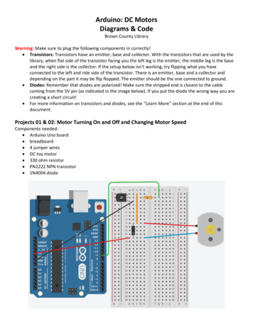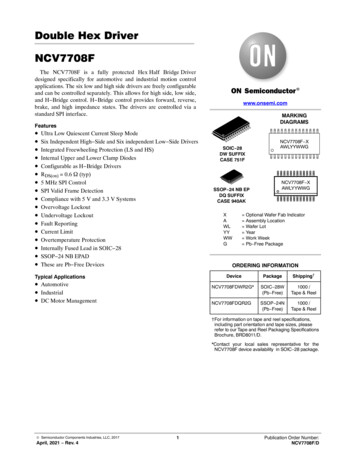
Transcription
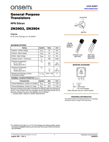
DATA SHEETwww.onsemi.comGeneral PurposeTransistorsCOLLECTOR3NPN Silicon2BASE2N3903, 2N39041EMITTERFeatures Pb Free Packages are Available*MAXIMUM RATINGSRatingSymbolValueUnitCollector Emitter VoltageVCEO40VdcCollector Base VoltageVCBO60VdcEmitter Base VoltageVEBO6.0VdcCollector Current ContinuousIC200mAdcTotal Device Dissipation@ TA 25 CDerate above 25 CPD6255.0mWmW/ CTotal Device Dissipation@ TC 25 CDerate above 25 CPD1.512WmW/ C 55 to 150 COperating and Storage JunctionTemperature RangeTJ, TstgTO 92CASE 29STYLE 11123STRAIGHT LEADBULK PACK23BENT LEADTAPE & REELAMMO PACKMARKING DIAGRAMS2N390xYWWGGTHERMAL CHARACTERISTICS (Note 1)CharacteristicSymbolMaxUnitThermal Resistance, Junction to AmbientRqJA200 C/WThermal Resistance, Junction to CaseRqJC83.3 C/WStresses exceeding those listed in the Maximum Ratings table may damage thedevice. If any of these limits are exceeded, device functionality should not beassumed, damage may occur and reliability may be affected.1. Indicates Data in addition to JEDEC Requirements.x 3 or 4Y YearWW Work WeekG Pb Free Package(Note: Microdot may be in either location)ORDERING INFORMATIONSee detailed ordering and shipping information in the packagedimensions section on page 3 of this data sheet.*For additional information on our Pb Free strategy and soldering details, pleasedownload the onsemi Soldering and Mounting Techniques Reference Manual,SOLDERRM/D. Semiconductor Components Industries, LLC, 2012August, 2021 Rev. 91Publication Order Number:2N3903/D
2N3903, 2N3904ELECTRICAL CHARACTERISTICS (TA 25 C unless otherwise noted)CharacteristicSymbolMinMaxUnitCollector Emitter Breakdown Voltage (Note 2) (IC 1.0 mAdc, IB 0)V(BR)CEO40 VdcCollector Base Breakdown Voltage (IC 10 mAdc, IE 0)V(BR)CBO60 VdcEmitter Base Breakdown Voltage (IE 10 mAdc, IC 0)V(BR)EBO6.0 VdcIBL 50nAdcICEX 50nAdc204035705010030601530 150300 0.20.30.65 0.850.95250300 OFF CHARACTERISTICSBase Cutoff Current (VCE 30 Vdc, VEB 3.0 Vdc)Collector Cutoff Current (VCE 30 Vdc, VEB 3.0 Vdc)ON CHARACTERISTICSDC Current Gain (Note 2)(IC 0.1 mAdc, VCE 1.0 042N39032N3904(IC 1.0 mAdc, VCE 1.0 Vdc)(IC 10 mAdc, VCE 1.0 Vdc)(IC 50 mAdc, VCE 1.0 Vdc)(IC 100 mAdc, VCE 1.0 Vdc)hFECollector Emitter Saturation Voltage (Note 2)(IC 10 mAdc, IB 1.0 mAdc)(IC 50 mAdc, IB 5.0 mAdcVCE(sat)Base Emitter Saturation Voltage (Note 2)(IC 10 mAdc, IB 1.0 mAdc)(IC 50 mAdc, IB 5.0 mAdc)VBE(sat) VdcVdcSMALL SIGNAL CHARACTERISTICSCurrent Gain Bandwidth Product(IC 10 mAdc, VCE 20 Vdc, f 100 MHz)2N39032N3904fTOutput Capacitance (VCB 5.0 Vdc, IE 0, f 1.0 MHz)Cobo 4.0Input Capacitance (VEB 0.5 Vdc, IC 0, f 1.0 MHz)Cibo 8.0Input Impedance(IC 1.0 mAdc, VCE 10 Vdc, f 1.0 kHz)2N39032N3904Voltage Feedback Ratio(IC 1.0 mAdc, VCE 10 Vdc, f 1.0 kHz)2N39032N3904Small Signal Current Gain(IC 1.0 mAdc, VCE 10 Vdc, f 1.0 1002004001.040 6.05.0td 35nstr 35nsts 175200nstf 50nshrehfeOutput Admittance (IC 1.0 mAdc, VCE 10 Vdc, f 1.0 kHz)hoeNoise Figure(IC 100 mAdc, VCE 5.0 Vdc, RS 1.0 k W, f 1.0 kHz)NF2N39032N3904MHzX 10 4 mmhosdBSWITCHING CHARACTERISTICSDelay TimeRise TimeStorage Time(VCC 3.0 Vdc, VBE 0.5 Vdc,IC 10 mAdc, IB1 1.0 mAdc)(VCC 3.0 Vdc, IC 10 mAdc,IB1 IB2 1.0 mAdc)2N39032N3904Fall Time2. Pulse Test: Pulse Width v 300 ms; Duty Cycle v 2%.www.onsemi.com2
2N3903, 2N3904ORDERING INFORMATIONPackageShipping†2N3903RLRMTO 922000 / Ammo Pack2N3904TO 925000 Units / BulkTO 92(Pb Free)5000 Units / BulkTO 922000 / Tape & ReelTO 92(Pb Free)2000 / Tape & ReelTO 922000 / Ammo PackTO 92(Pb Free)2000 / Ammo PackTO 922000 / Ammo Pack2N3904RLRPGTO 92(Pb Free)2000 / Ammo Pack2N3904RL1GTO 92(Pb Free)2000 / Tape & ReelTO 922000 / Ammo PackTO 92(Pb Free)2000 / Ammo 3904RLRMG2N3904RLRP2N3904ZL12N3904ZL1G†For information on tape and reel specifications, including part orientation and tape sizes, please refer to our Tape and Reel PackagingSpecifications Brochure, BRD8011/D.DUTY CYCLE 2%300 ns 3 V 10.9 V27510 k- 0.5 VCS 4 pF* 1 ns* Total shunt capacitance of test jig and connectorsFigure 1. Delay and Rise Time Equivalent Test Circuit10 t1 500 msDUTY CYCLE 2%t1 3 V 10.9 V27510 k01N916- 9.1 V′CS 4 pF* 1 ns* Total shunt capacitance of test jig and connectorsFigure 2. Storage and Fall Time Equivalent Test Circuitwww.onsemi.com3
2N3903, 2N3904TYPICAL TRANSIENT CHARACTERISTICSTJ 25 CTJ 125 C10500020005.0Q, CHARGE (pC)CAPACITANCE (pF)VCC 40 VIC/IB .2 0.30.5 0.7 1.02.0 3.05.0 7.0 10100705020 30 402.0 3.05.0 7.0 10203050 70 100REVERSE BIAS VOLTAGE (VOLTS)IC, COLLECTOR CURRENT (mA)Figure 3. CapacitanceFigure 4. Charge Data500200500IC/IB 1010070tr @ VCC 3.0 V503020VCC 40 VIC/IB 10300200t r, RISE TIME (ns)300200TIME (ns)1.040 V1007050302015 V1075102.0 Vtd @ VOB 0 V1.02.0 3.05.0 7.0 10203050 70 1001.02.0 3.05.0 7.0 10203050 70 100IC, COLLECTOR CURRENT (mA)Figure 5. Turn On TimeFigure 6. Rise TimeIC/IB 10200500t′s ts - 1/8 tfIB1 IB2VCC 40 VIB1 IB2300200IC/IB 20t f , FALL TIME (ns)t s′ , STORAGE TIME (ns)IC/IB 20200IC, COLLECTOR CURRENT (mA)5003002007510070IC/IB 2050IC/IB 1030201007050101075751.02.0 3.05.0 7.0 10203050 70 100200IC/IB 1030201.02.0 3.05.0 7.0 10203050 70 100IC, COLLECTOR CURRENT (mA)IC, COLLECTOR CURRENT (mA)Figure 7. Storage TimeFigure 8. Fall Timewww.onsemi.com4200
2N3903, 2N3904TYPICAL AUDIO SMALL SIGNAL CHARACTERISTICSNOISE FIGURE VARIATIONS(VCE 5.0 Vdc, TA 25 C, Bandwidth 1.0 Hz)1412SOURCE RESISTANCE 200 WIC 1.0 mAf 1.0 kHzSOURCE RESISTANCE 200 WIC 0.5 mA86SOURCE RESISTANCE 1.0 kIC 50 mA4SOURCE RESISTANCE 500 WIC 100 mA200.10.20.41.02.0IC 1.0 mA12NF, NOISE FIGURE (dB)NF, NOISE FIGURE (dB)10IC 0.5 mA10IC 50 mA8IC 100 mA6424.010204001000.10.20.41.02.04.01020f, FREQUENCY (kHz)RS, SOURCE RESISTANCE (k OHMS)Figure 9.Figure 10.401005.0105.010h PARAMETERS(VCE 10 Vdc, f 1.0 kHz, TA 25 C)100hoe, OUTPUT ADMITTANCE (m mhos)h fe , CURRENT GAIN3002001007050300.10.20.30.51.02.0 3.0IC, COLLECTOR CURRENT (mA)5.0502010521100.10.2Figure 11. Current GainFigure 12. Output Admittanceh re , VOLTAGE FEEDBACK RATIO (X 10 -4 )h ie , INPUT IMPEDANCE (k OHMS)20105.02.01.00.50.20.10.20.30.51.02.0 3.0IC, COLLECTOR CURRENT (mA)0.30.51.02.0 3.0IC, COLLECTOR CURRENT (mA)5.0107.05.03.02.01.00.70.5100.1Figure 13. Input Impedance0.20.30.51.02.0 3.0IC, COLLECTOR CURRENT (mA)Figure 14. Voltage Feedback Ratiowww.onsemi.com5
2N3903, 2N3904h FE, DC CURRENT GAIN (NORMALIZED)TYPICAL STATIC CHARACTERISTICS2.0TJ 125 CVCE 1.0 V 25 C1.00.7- 55 050100200IC, COLLECTOR CURRENT (mA)VCE, COLLECTOR EMITTER VOLTAGE (VOLTS)Figure 15. DC Current Gain1.0TJ 25 C0.8IC 1.0 mA10 mA30 mA100 2.03.05.07.010IB, BASE CURRENT (mA)Figure 16. Collector Saturation Region1.01.2TJ 25 CVBE(sat) @ IC/IB 100.8VBE @ VCE 1.0 V0.60.4VCE(sat) @ IC/IB 10qVC FOR VCE(sat)0- 55 C TO 25 C- 0.5- 55 C TO 25 C- 1.0 25 C TO 125 CqVB FOR VBE(sat)- 1.50.20 25 C TO 125 C0.5COEFFICIENT (mV/ C)V, VOLTAGE (VOLTS)1.01.02.05.0102050100- 2.0200020406080100120140160IC, COLLECTOR CURRENT (mA)IC, COLLECTOR CURRENT (mA)Figure 17. “ON” VoltagesFigure 18. Temperature Coefficientswww.onsemi.com6180 200
MECHANICAL CASE OUTLINEPACKAGE DIMENSIONSTO 92 (TO 226)CASE 29 11ISSUE AMSCALE 1:11123STRAIGHT LEADBULK PACKDATE 09 MAR 200723BENT LEADTAPE & REELAMMO PACKABNOTES:1. DIMENSIONING AND TOLERANCING PER ANSIY14.5M, 1982.2. CONTROLLING DIMENSION: INCH.3. CONTOUR OF PACKAGE BEYOND DIMENSION RIS UNCONTROLLED.4. LEAD DIMENSION IS UNCONTROLLED IN P ANDBEYOND DIMENSION K MINIMUM.STRAIGHT LEADBULK PACKRPLSEATINGPLANEKDIMABCDGHJKLNPRVDX XGJHVCSECTION X OTES:1. DIMENSIONING AND TOLERANCING PERASME Y14.5M, 1994.2. CONTROLLING DIMENSION: MILLIMETERS.3. CONTOUR OF PACKAGE BEYONDDIMENSION R IS UNCONTROLLED.4. LEAD DIMENSION IS UNCONTROLLED IN PAND BEYOND DIMENSION K MINIMUM.BENT LEADTAPE & REELAMMO PACKBPTSEATINGPLANEGKDIMABCDGJKNPRVDX XJV1CNSECTION X --STYLES ON PAGE 2DOCUMENT NUMBER:STATUS:98ASB42022BON SEMICONDUCTOR STANDARDNEW STANDARD: Semiconductor Components Industries, LLC, 2002October, DESCRIPTION:2002 Rev. 0TO 92 (TO 226)http://onsemi.com1Electronic versions are uncontrolled except whenaccessed directly from the Document Repository. Printedversions are uncontrolled except when stamped“CONTROLLED COPY” in red.Case Outline Number:PAGE 1 OFXXX3
TO 92 (TO 226)CASE 29 11ISSUE AMDATE 09 MAR 2007STYLE 1:PIN 1. EMITTER2. BASE3. COLLECTORSTYLE 2:PIN 1. BASE2. EMITTER3. COLLECTORSTYLE 3:PIN 1. ANODE2. ANODE3. CATHODESTYLE 4:PIN 1. CATHODE2. CATHODE3. ANODESTYLE 5:PIN 1. DRAIN2. SOURCE3. GATESTYLE 6:PIN 1. GATE2. SOURCE & SUBSTRATE3. DRAINSTYLE 7:PIN 1. SOURCE2. DRAIN3. GATESTYLE 8:PIN 1. DRAIN2. GATE3. SOURCE & SUBSTRATESTYLE 9:PIN 1. BASE 12. EMITTER3. BASE 2STYLE 10:PIN 1. CATHODE2. GATE3. ANODESTYLE 11:PIN 1. ANODE2. CATHODE & ANODE3. CATHODESTYLE 12:PIN 1. MAIN TERMINAL 12. GATE3. MAIN TERMINAL 2STYLE 13:PIN 1. ANODE 12. GATE3. CATHODE 2STYLE 14:PIN 1. EMITTER2. COLLECTOR3. BASESTYLE 15:PIN 1. ANODE 12. CATHODE3. ANODE 2STYLE 16:PIN 1. ANODE2. GATE3. CATHODESTYLE 17:PIN 1. COLLECTOR2. BASE3. EMITTERSTYLE 18:PIN 1. ANODE2. CATHODE3. NOT CONNECTEDSTYLE 19:PIN 1. GATE2. ANODE3. CATHODESTYLE 20:PIN 1. NOT CONNECTED2. CATHODE3. ANODESTYLE 21:PIN 1. COLLECTOR2. EMITTER3. BASESTYLE 22:PIN 1. SOURCE2. GATE3. DRAINSTYLE 23:PIN 1. GATE2. SOURCE3. DRAINSTYLE 24:PIN 1. EMITTER2. COLLECTOR/ANODE3. CATHODESTYLE 25:PIN 1. MT 12. GATE3. MT 2STYLE 26:PIN 1. VCC2. GROUND 23. OUTPUTSTYLE 27:PIN 1. MT2. SUBSTRATE3. MTSTYLE 28:PIN 1. CATHODE2. ANODE3. GATESTYLE 29:PIN 1. NOT CONNECTED2. ANODE3. CATHODESTYLE 30:PIN 1. DRAIN2. GATE3. SOURCESTYLE 31:PIN 1. GATE2. DRAIN3. SOURCESTYLE 32:PIN 1. BASE2. COLLECTOR3. EMITTERSTYLE 33:PIN 1. RETURN2. INPUT3. OUTPUTSTYLE 34:PIN 1. INPUT2. GROUND3. LOGICSTYLE 35:PIN 1. GATE2. COLLECTOR3. EMITTERDOCUMENT NUMBER:STATUS:98ASB42022BON SEMICONDUCTOR STANDARDNEW STANDARD: Semiconductor Components Industries, LLC, 2002October, DESCRIPTION:2002 Rev. 0TO 92 (TO 226)http://onsemi.com2Electronic versions are uncontrolled except whenaccessed directly from the Document Repository. Printedversions are uncontrolled except when stamped“CONTROLLED COPY” in red.Case Outline Number:PAGE 2 OFXXX3
DOCUMENT NUMBER:98ASB42022BPAGE 3 OF 3ISSUEAMREVISIONADDED BENT LEAD TAPE & REEL VERSION. REQ. BY J. SUPINA.DATE09 MAR 2007ON Semiconductor andare registered trademarks of Semiconductor Components Industries, LLC (SCILLC). SCILLC reserves the right to make changes without further noticeto any products herein. SCILLC makes no warranty, representation or guarantee regarding the suitability of its products for any particular purpose, nor does SCILLC assume any liabilityarising out of the application or use of any product or circuit, and specifically disclaims any and all liability, including without limitation special, consequential or incidental damages.“Typical” parameters which may be provided in SCILLC data sheets and/or specifications can and do vary in different applications and actual performance may vary over time. Alloperating parameters, including “Typicals” must be validated for each customer application by customer’s technical experts. SCILLC does not convey any license under its patent rightsnor the rights of others. SCILLC products are not designed, intended, or authorized for use as components in systems intended for surgical implant into the body, or other applicationsintended to support or sustain life, or for any other application in which the failure of the SCILLC product could create a situation where personal injury or death may occur. ShouldBuyer purchase or use SCILLC products for any such unintended or unauthorized application, Buyer shall indemnify and hold SCILLC and its officers, employees, subsidiaries, affiliates,and distributors harmless against all claims, costs, damages, and expenses, and reasonable attorney fees arising out of, directly or indirectly, any claim of personal injury or deathassociated with such unintended or unauthorized use, even if such claim alleges that SCILLC was negligent regarding the design or manufacture of the part. SCILLC is an EqualOpportunity/Affirmative Action Employer. This literature is subject to all applicable copyright laws and is not for resale in any manner. Semiconductor Components Industries, LLC, 2007March, 2007 Rev. 11AMCase Outline Number:29
onsemi,, and other names, marks, and brands are registered and/or common law trademarks of Semiconductor Components Industries, LLC dba “onsemi” or its affiliatesand/or subsidiaries in the United States and/or other countries. onsemi owns the rights to a number of patents, trademarks, copyrights, trade secrets, and other intellectual property.A listing of onsemi’s product/patent coverage may be accessed at www.onsemi.com/site/pdf/Patent Marking.pdf. onsemi reserves the right to make changes at any time to anyproducts or information herein, without notice. The information herein is provided “as is” and onsemi makes no warranty, representation or guarantee regarding the accuracy of theinformation, product features, availability, functionality, or suitability of its products for any particular purpose, nor does onsemi assume any liability arising out of the application or useof any product or circuit, and specifically disclaims any and all liability, including without limitation special, consequential or incidental damages. Buyer is responsible for its productsand applications using onsemi products, including compliance with all laws, regulations and safety requirements or standards, regardless of any support or applications informationprovided by onsemi. “Typical” parameters which may be provided in onsemi data sheets and/or specifications can and do vary in different applications and actual performance mayvary over time. All operating parameters, including “Typicals” must be validated for each customer application by customer’s technical experts. onsemi does not convey any licenseunder any of its intellectual property rights nor the rights of others. onsemi products are not designed, intended, or authorized for use as a critical component in life support systemsor any FDA Class 3 medical devices or medical devices with a same or similar classification in a foreign jurisdiction or any devices intended for implantation in the human body. ShouldBuyer purchase or use onsemi products for any such unintended or unauthorized application, Buyer shall indemnify and hold onsemi and its officers, employees, subsidiaries, affiliates,and distributors harmless against all claims, costs, damages, and expenses, and reasonable attorney fees arising out of, directly or indirectly, any claim of personal injury or deathassociated with such unintended or unauthorized use, even if such claim alleges that onsemi was negligent regarding the design or manufacture of the part. onsemi is an EqualOpportunity/Affirmative Action Employer. This literature is subject to all applicable copyright laws and is not for resale in any manner.PUBLICATION ORDERING INFORMATIONLITERATURE FULFILLMENT:Email Requests to: orderlit@onsemi.comonsemi Website: www.onsemi.com TECHNICAL SUPPORTNorth American Technical Support:Voice Mail: 1 800 282 9855 Toll Free USA/CanadaPhone: 011 421 33 790 2910Europe, Middle East and Africa Technical Support:Phone: 00421 33 790 2910For additional information, please contact your local Sales Representative
2N3903, 2N3904 www.onsemi.com 2 ELECTRICAL CHARACTERISTICS (TA 25 C unless otherwise noted) Characteristic Symbol Min Max Unit OFF CHARACTERISTICS Collector Emitter Breakdown Voltage (Note 2) (IC 1.0 mAdc, IB 0) V(BR)CEO 40 Vdc Collector Base Breakdown Voltage (IC 10 Adc, IE 0) V(BR)CBO 60 Vdc Emitter Base Breakdown Voltage (IE 10 Adc, IC 0) V(BR)EBO 6.0 Vdc