Transcription
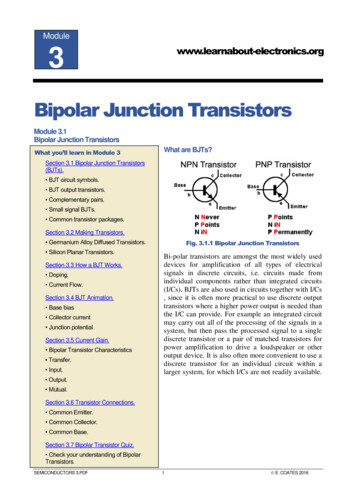
Modulewww.learnabout-electronics.org3Bipolar Junction TransistorsModule 3.1Bipolar Junction TransistorsWhat you’ll learn in Module 3What are BJTs?Section 3.1 Bipolar Junction Transistors(BJTs). BJT circuit symbols. BJT output transistors. Complementary pairs. Small signal BJTs. Common transistor packages.Section 3.2 Making Transistors.Fig. 3.1.1 Bipolar Junction Transistors Germanium Alloy Diffused Transistors. Silicon Planar Transistors.Section 3.3 How a BJT Works. Doping. Current Flow.Section 3.4 BJT Animation. Base bias Collector current Junction potentialSection 3.5 Current Gain. Bipolar Transistor Characteristics Transfer. Input.Bi-polar transistors are amongst the most widely useddevices for amplification of all types of electricalsignals in discrete circuits, i.e. circuits made fromindividual components rather than integrated circuits(I/Cs). BJTs are also used in circuits together with I/Cs, since it is often more practical to use discrete outputtransistors where a higher power output is needed thanthe I/C can provide. For example an integrated circuitmay carry out all of the processing of the signals in asystem, but then pass the processed signal to a singlediscrete transistor or a pair of matched transistors forpower amplification to drive a loudspeaker or otheroutput device. It is also often more convenient to use adiscrete transistor for an individual circuit within alarger system, for which I/Cs are not readily available. Output. Mutual.Section 3.6 Transistor Connections. Common Emitter. Common Collector. Common Base.Section 3.7 Bipolar Transistor Quiz. Check your understanding of BipolarTransistors.SEMICONDUCTORS 3.PDF1 E. COATES 2016
www.learnabout-electronics.orgSemiconductors Module 3 Bipolar Junction TransistorsTransistors come in many shapes and types. A selection of typical bipolar junction transistors(BJTs) is shown in Fig 3.1.2 1. BUH515High Voltage (1500V) high power (50W)NPN fast switching transistor in anISOWATT218 package, originally designedfor use in analogue TV timebases but alsoused in switched mode power supplies.2. 2N3055NPN Silicon Power transistor (115W)designed for switching and amplifierapplications. Can be used as one half of acomplementary push-pull output pair withthe PNP MJ2955 transistor.3. 2N2219NPN silicon transistor in a metal casedTO-39 package, designed for use as a highspeed switch or for amplification atfrequencies from DC (0Hz) up to UHF atabout 500MHz.4. 2N6487General purpose NPN output transistorwith a power rating up to 75W in a TO-220package.5. BD135/BD136Complementary (NPN/PNP) pair of lowmedium power audio output transistors in aSOT-32 package.Fig. 3.1.2 Typical Bipolar Junction Transistors6, 7 and 8. 2N222Small signal general purpose amplifier and switching transistors like the 2N2222 and 2N3904 arecommonly available in a variety of package types such as the TO-18 metal cased package (6), and thecheaper plastic TO-92 version (7) for through-hole mounting on printed circuit boards, as well as in surfacemount SOT-23 versions (8).Many transistor package types are also available withalternative connection layouts. The TO-92 package forexample has variants TO-94, TO-96, TO-97 and TO-98all with similar physical appearance, but each with adifferent pin configuration. Where different packagevariants are available, these are usually identified on thedata sheet for each particular transistor type. Typicalvariations, such as those for the TO-92 to 98 series ofpackages used for transistors such as the 2N2222 areillustrated in Fig. 3.1.3.SEMICONDUCTORS MODULE 3 PDF2Fig. 3.1.3 TO-92 package variations E. COATES 2020
www.learnabout-electronics.orgSemiconductors Module 3 Bipolar Junction TransistorsModule 3.2How Transistors Are MadeWhat you’ll learn in Module 3.2After studying this section, you should be able to: Recognise alloy diffused & silicon planartransistors. Recognise the advantages of silicon planartechnology. Describe the basic steps in planar transistormanufacture.Fig 3.2.1 Germanium AlloyDiffused TransistorAlloy Diffused TransistorsEarly bipolar junction transistors used a variety of methods to produce a currentamplifier. Typically a thin wafer of Germanium was used for the base of the transistor.The emitter and collector were made by diffusing two pellets of Indium (a trivalentmaterial, having three electrons in their valence shell) into either side of a wafer of Ntype base, as shown in Fig 3.2.1.The fusion process causes the indium to diffuse into the germanium. As the two metals fusetogether indium atoms (with 3 valence electrons) mix with the pure germanium atoms (with 4valence electrons) creating P type material where the Indium atoms will appear to be short of oneelectron, and so will bond with only three instead of four neighbouring atoms. This creates a "hole"charge carrier at each Indium atom. Fusing is stopped just before the two P type regions meet. Theresult is an extremely thin layer of N type semiconductor (the BASE) sandwiched between twothicker P type layers, which form the other two terminals, the emitter and the collector. Notice thatthe P type region used for the collector is larger than the emitter region. This is because most of theheat generated within the transistor is generated at the base/collector junction. This junctiontherefore needs to be larger to dissipate this extra heat.Alloy diffused transistors suffer from several drawbacks:1. They have a poor frequency response due mainly to their large junction capacitances.2. Their collector current increases as their temperature increases, making them susceptible todestruction due to thermal runaway.3. They have relatively high leakage currents acrossthe junctions.4. They cannot withstand high voltages.Silicon Planar TransistorsThe disadvantages of diffused alloy transistors wasovercome in the 1950s by developing transistors that usesilicon as the semiconductor material and the planar(layered) type of construction, illustrated in Figures 3.2.2to 3.2.3 These transistors are built up as a series of verythin layers (or planes) of semiconductor material built uprather like a multi layer sandwich). Construction is morecomplex than the alloy diffusion technique, requiringSEMICONDUCTORS MODULE 3 PDF3Fig 3.2.2 Multi Layer Constructionof a Silicon Planar Transistor. E. COATES 2020
www.learnabout-electronics.orgSemiconductors Module 3 Bipolar Junction Transistorsmany separate steps, depositing oxide layers on the silicon wafer and using photo lithographictechniques to etch away unwanted silicon areas. These steps are repeated with variations to build upthe required patterns and layers to form either individual transistors or complete interconnectedintegrated circuits.Although the many individual manufacturing steps are complex, from forming an ingot of very puresilicon, slicing it into wafers and forming the required components on the wafer, thousands oftransistors can be made at the same time on a single wafer of silicon, this method of constructionthen becomes much cheaper and more reliable than the ‘one transistor at a time’ alloy diffusionmethod.Once the transistors have been formed on the wafer, each one is tested automatically and any faultytransistors are marked with a spot of dye. The wafer is then cut up into the individual transistors andthose marked as faulty are discarded.The planar process is even more efficient when used to manufacture integrated circuits wherenumbers of interconnected transistors are fabricated on a single chip of silicon at the same time. Theintegrated circuits produced by this method may contain just a few interconnected transistors (SmallScale Integration or SSI), hundreds of transistors (Medium Scale Integration or MSI), thousands oftransistors (Large Scale Integration or LSI), or devices such as microprocessors with millions ofinterconnected transistors (Very Large Scale Integration or VLSI). Figs. 3.2.2 to 3.2.4 illustrate thebasic steps in the manufacturing process, assuming a wafer populated with single transistors.1. Layer 1 - Heavily doped N type Silicon.2. Lightly doped N type silicon is deposited ontop of layer 1 making a two layer collector.(see "How BJTs Work").3. Part of the collector layer is etched away toform a depression for the P type base layer.4. P type base layer is added.5. Part of the base layer is etched away leavinga very thin base layer.6. A heavily doped N type emitter layer isadded.Fig 3.2.3 The Planar Construction Process.7. Finally metal connectors are added allowing leads to be fixed after testing, and separating fromthe wafer.Fig 3.2.4 Completed Silicon Planar Transistor.SEMICONDUCTORS MODULE 3 PDF4 E. COATES 2020
www.learnabout-electronics.orgSemiconductors Module 3 Bipolar Junction TransistorsModule 3.3How a BJT (Bipolar Junction Transistor) WorksWhat you’ll learn in Module 3.3After studying this section, you should be able to: Describe the basic operation of a silicon planartransistor. Understand the operation of the base/emitter andbase/collector junctions. Describe the effects of doping in the transistormaterials.Fig 3.3.2 How a Transistor Amplifies CurrentIt’s all in the dopingThe way a transistor works can be described with referenceto Fig. 3.3.1, which shows the basic doping of a junctiontransistor and Fig. 3.3.2 showing how the BJT works.Fig 3.3.1 How a Transistor is DopedThe operation of the transistor is very dependent on the degree of doping of the various parts of the semiconductorcrystal. The N type emitter is very heavily doped to provide many free electrons as majority charge carriers. Thelightly doped P type base region is extremely thin, and the N type collector is very heavily doped to give it a lowresistivity apart from a layer of less heavily doped material near to the base region. This change in the resistivity ofthe collector, ensures that a large potential is present within the collector material close to the base. The importanceof this will become apparent from the following description.During normal operation, a potential isapplied across the base/emitterjunction so that the base isapproximately 0.6V more positive thanthe emitter, this makes thebase/emitter junction forward biased.A much higher potential is appliedacross the base/collector junction witha relatively high positive voltageapplied to the collector, so that thebase/collector junction is heavilyreverse biased. This makes thedepletion layer between base andcollector quite wide once power isFig 3.3.2 How a Transistor Amplifies Currentapplied. As mentioned above, thecollector is made up of mainly heavilydoped, low resistivity material with a thin layer of lightly doped, high resistivity material next to the base/collectorjunction. This means that most of the voltage between collector and base is developed across this thin highresistivity layer, creating a high voltage gradient near the collector base junction.When the base emitter junction is forward biased, a small current will flow into the base. Therefore holes areinjected into the P type material. These holes attract electrons across the forward biased base/emitter junction tocombine with the holes. However, because the emitter region is very heavily doped, many more electrons crossinto the P type base region than are able to combine with the available holes. This means there is a largeconcentration of electrons in the base region and most of these electrons are swept straight through the very thinbase, and into the base/collector depletion layer. Once here, they come under the influence of the strong electricfield across the base/collector junction. This field is so strong due to the large potential gradient in the collectormaterial mentioned earlier, that the electrons are swept across the depletion layer and into the collector material,and so towards the collector terminal.Varying the current flowing into the base, affects the number of electrons attracted from the emitter.In this way verysmall changes in base current cause very large changes in the current flowing from emitter to collector, so currentamplification is taking place.SEMICONDUCTORS MODULE 3 PDF5 E. COATES 2020
www.learnabout-electronics.orgSemiconductors Module 3 Bipolar Junction TransistorsModule 3.4BJT VideoWhat you’ll learn in Module 3.4After studying this section, you should be able to: Describe the basic operation of a silicon planartransistor. Understand the effect of varying the base/emitter andbase/collector potentials. Describe the action of charge carriers in the transistor.Our video illustrating how a BJT is made and how it operates is available at:A full screen version can be downloaded from the conductors/bjt 04.phpSEMICONDUCTORS MODULE 3 PDF6 E. COATES 2020
www.learnabout-electronics.orgSemiconductors Module 3 Bipolar Junction TransistorsModule 3.5Current GainA BJT is a current operated transistor,which means that the current flowingbetween emitter and collector of atransistor is much greater than thatflowing between base and emitter. So a small basecurrent is controlling the much largercollector/emitter current. The ratio of the twocurrents, ICE / IBE is constant, provided that thecollector emitter voltage VCE is constant. Therefore,if the base current rises, so does collector current.What you’ll learn in Module 3.5After studying this section, you should beable to:Understand the use of common transistorcharacteristic graphs. Transfer Characteristics. Input & Output Characteristics. Mutual Characteristics.In describing the operation of junction transistors.The BJT Transfer CharacteristicThis ratio is the CURRENT GAIN of the transistor and is giventhe symbol hfe. A fairly low gain transistor might have a currentgain of 20 to 50, while a high gain type may have a gain of 300to 800 or more. The spread of values of hfe for any giventransistor is quite large, even in transistors of the same type andbatch. The graph of ICE / IBE shown in Fig. 3.5.1 is called theTRANSFER CHARACTERISTIC and the slope of the graphshows the hfe for that transistorFig. 3.5.1 Transfer CharacteristicCharacteristic curves (graphs) can be drawn to show other parameters of a transistor, and are usedboth to detail the performance of a particular device and as an aid to the design of amplifiers. Theexamples shown here are typical of BJTs, when used as voltage amplifiers.The BJT Input CharacteristicThe INPUT CHARACTERISTIC (Fig.3.5.2), a graph of baseemitter current IBE against base emitter voltage VBE (IBE/VBE)shows the input CONDUCTANCE of the transistor. Asconductance I/V is the reciprocal of RESISTANCE (V/I) thiscurve can be used to determine the input resistance of thetransistor. The steepness of this particular curve when the VBE isabove 1 volt shows that the input conductance is very high, andthere is a large increase in current (in practice, usually enough todestroy the transistor!) for a very small increase in VBE. Thereforethe input RESISTANCE must be low. Around 0.6 to 0.7 volts thegraph , showing that the input resistance of a transistor varies,according to the amount of base current flowing, and below about0.5 volts base current ceases.SEMICONDUCTORS MODULE 3 PDF7Fig. 3.5.2 Input Characteristic E. COATES 2020
www.learnabout-electronics.orgSemiconductors Module 3 Bipolar Junction TransistorsThe BJT Output CharacteristicFig. 3.5.3 shows the OUTPUT CHARACTERISTIC whoseslope gives the value of output conductance (and byimplication output resistance). The near horizontal parts of thegraph lines show that a change in collector emitter voltage VCEhas almost no effect on collector current in this region, just theeffect to be expected if the transistor output had a large valueresistor in series with it. Therefore the graph shows that theoutput resistance of the transistor is high.These characteristic graphs show that, for a silicon transistorwith an input applied between base and emitter, and outputtaken between collector and emitter (a method of connectioncalled common emitter mode) one would expect;Fig. 3.5.3 Output Characteristic Low input resistance (from the input characteristic). Fairly high gain (from the transfer characteristic). High output resistance (from the output characteristic).The BJT Mutual CharacteristicFig. 3.5.4, the MUTUAL CHARACTERISTIC shows agraph of MUTUAL CONDUCTANCE IC/VBE andillustrates the change in collector current which takes placefor a given change in base emitter voltage, (i.e. input signalvoltage). This graph is for a typical silicon power transistor.Notice the large collector currents possible, and the nearlylinear relationship between the input voltage and outputcurrent.The characteristics described on this page are those relatingto a typical power transistor connected in the ‘common Fig. 3.5.4 Mutual Characteristicemitter’ mode. This is one of three possible modes ofconnection for a transistor described in BJT Module 3.6. - Transistor Connections.Note: In many transistors the currents will be much smaller than shown in these examples. Forsmall signal amplifiers, base currents will be a few micro-amps rather than milliamps.SEMICONDUCTORS MODULE 3 PDF8 E. COATES 2020
www.learnabout-electronics.orgSemiconductors Module 3 Bipolar Junction TransistorsModule 3.6Transistor ConnectionsWhat you’ll learn in Module 3.6After studying this section, youshould be able to:Recognise basic transistor amplifierconnection modes. Common emitter. Common collector. Common base.Describe the basic parameters ofeach amplifier mode.How a transistor is connected to make an amplifier.Because an amplifiermust have two input andtwo output terminals, atransistor used as anamplifier must have oneof its three terminalscommon to both input Fig. 3.6.1 Amplifier Connectionsand output as shown inFig 3.6.1. The choice of which terminal is used as thecommon connection has a marked effect on the performanceof the amplifier. Voltage gain.A transistor connected in the three modes illustrated in Figs.3.6.2 to 3.6.4 would show quite different characteristic curves Input & output impedances.for each mode. These differences can be exploited by thecircuit designer to give an amplifier with characteristics thatare most suited a particular purpose. Note that the diagrams are shown here reduced to their mostbasic form and are not intended to be practical circuits. Current gain.In a transistor amplifier circuit, such as those shown in Figs. 3.6.2 to 3.6.4, the V supply line andthe 0V line can be considered as the same point, as far as any AC signal is concerned. This isbecause, although there is obviously a voltage (the supply voltage) between these two points, theDC supply is always de-coupled by a large capacitor (e.g. the reservoir capacitor in the powersupply) so there can be no AC voltage difference between V and 0V rails.Common Emitter ModeThe most common function of a transistor is to be used inCOMMON EMITTER mode. In this method of connection smallchanges in base/emitter current cause large changes incollector/emitter current. Therefore the circuit is that of aCURRENT amplifier. To give VOLTAGE amplification, a loadresistor (or an impedance such as a tuned circuit) must beconnected in the collector circuit, so that a change in collectorcurrent causes a change in the voltage developed across the loadresistor. The value of the load resistor will affect the VOLTAGEGAIN of the amplifier. This is because the larger the load resistor,the larger the change in voltage that will be caused by a givenchange in collector current. Notice that because of this method ofFig. 3.6.2 Common Emitter Modeconnection the output waveform will be in anti-phase to the inputwaveform. This is because an increase in base/emitter voltage will cause an increase in base current.This will in turn cause an increase in collector current, but as collector current increases, the voltagedrop across the load resistor increases and as the voltage on the top end of the load resistor (thesupply voltage) will not change, the voltage on the bottom end must decrease. Therefore an increasein base/emitter voltage causes a decrease in collector/emitter voltage.Common Emitter ParametersVoltage Gain: High (about 100).Current Gain: High (about 50 to 800).Input Impedance: Medium (about 3kΩ to 5kΩ).Output Impedance: Medium (Approximately the load resistor value).SEMICONDUCTORS MODULE 3 PDF9 E. COATES 2020
www.learnabout-electronics.orgFig. 3.6.3 Common Collector ModeSemiconductors Module 3 Bipolar Junction TransistorsCommon Collector ModeFig. 3.6.3 illustrates the COMMON COLLECTOR mode; also calledthe emitter follower mode as in this circuit the output waveform atthe emitter is not inverted and so ‘follows’ the input waveform at thebase. This method of connection is often used as a BUFFERAMPLIFIER for such jobs as matching impedances between twoother circuits. This is because this mode gives the amplifier a highinput impedance and a low output impedance. The voltage gain inthis mode is slightly less than unity (x 1), but high current gain(called hfc in common collector mode) is available. Another use forthis mode of connection is a CURRENT AMPLIFIER, often used foroutput circuits that have to drive high current AC devices such asloudspeakers or DC devices such as motors etc.Common Collector ParametersVoltage Gain: Slightly less than unity (1).Current Gain: High (about 50 to 800)Input Impedance: High (Several kΩ)Output Impedance: Low (A few ohms)Common Base ModeCOMMON BASE MODE is usually used for VHF and UHFamplifiers where, although the voltage gain is not high, there is littlechance of the output signal being fed back into the input circuit(which can be a problem at these frequencies). Because the base ofthe transistor is connected to ground in this mode, it forms aneffective grounded (earthed) screen between output and input. As thecollector current in this mode will be the emitter current minus thebase current, the current gain (hfb in common base mode) is less thanunity ( 1).Fig. 3.6.4 Common Base ModeCommon Base ParametersVoltage Gain: Medium (about 10 to 50).Current Gain: Less than unity ( 1)Input Impedance: Low (about 50Ω)Output Impedance: High (about 1MΩ)SEMICONDUCTORS MODULE 3 PDF10 E. COATES 2020
www.learnabout-electronics.orgSemiconductors Module 3 Bipolar Junction TransistorsModule 3.7Bipolar Junction Transistor QuizTry this quiz based on bipolar transistors. All the information you need is onhttp://www.learnabout-electronics.orgYou can answer the questions here, but to check your answers go to Semiconductors Module 3.7 onthe website. Hopefully your answers will all be correct, but don't be disappointed if you get someanswers wrong. Follow the hints on the website results page to find the right answer, and learn moreabout transistors as you go.1.In a BJT, why is a thin layer of high resistivity semiconductor included between the base and collectorregions?a) To create a high voltage gradient between the base and collector regions.b) To help prevent collector/base breakdown.c) To ensure the voltage difference between base and collector is kept as low as possible.d) To prevent holes contaminating the N type collector region.2.The forward junction potential for a silicon junction is:a) 0.015 Voltsb) 0.15 Voltsc) 0.06 Voltsd) 0.6 Volts3.Refer to Fig. 3.7.1. What do the graphs shown illustrate?a) The transfer characteristics of a BJT in common emitter mode.b) The output characteristics of a BJT in common emitter mode.c) The transfer characteristics of a BJT in common collector mode.d) The mutual characteristics of a BJT in common emitter mode.4.For a NPN silicon bipolar transistor, which of the following statementsis true?a) A thin area of the collector near to the base is heavily doped.b) A thin area of the emitter near to the base is heavily doped.c) The resistivity of the collector decreases near to the base.d) A thin area of the collector near to the base is lightly doped.SEMICONDUCTORS MODULE 3 PDF11 E. COATES 2020
www.learnabout-electronics.orgSemiconductors Module 3 Bipolar Junction Transistors5.The formula for the small signal current gain of a bipolar transistor is given by:a) ICE / IBEb) Ice / Ibec) Ice / Vbed) ICE / VBE6.When testing the resistance of a junction in a silicon bipolar transistor, the expected junction resistance,when forward biased will be approximately:a) 1k Ohmsb) 5k Ohmsc) Infinited) Zero Ohms7.The voltage gain of a bipolar transistor used in Common Collector (emitter follower) mode will be:a) About 50 to 100b) About 50 to 800c) 1 (Unity)d) Several thousand8.The number of valence electrons in a silicon atom is:a) Threeb) Fivec) Eightd) Four9.To increase the number of free electrons in silicon for use in transistors, manufacturers add smallamounts of:a) Germaniumb) Aluminiumc) Borond) ArsenicSEMICONDUCTORS MODULE 3 PDF12 E. COATES 2020
www.learnabout-electronics.orgSemiconductors Module 3 Bipolar Junction Transistors10.When identifying the connections on a large power transistor, a useful tip to remember is:a) The base is always the middle pin.b) The collector is usually identified by a metal tab or paint spot.c) The collector is usually connected to the metal case.d) The resistance measured between emitter and the metal case will be zero ohms.SEMICONDUCTORS MODULE 3 PDF13 E. COATES 2020
transistors where a higher power output is needed than the I/C can provide. For example an integrated circuit may carry out all of the processing of the signals in a system, but then pass the processed signal to a single discrete transistor or a pair of matched transistors for power amplification to drive a loudspeaker or other output device.