Transcription
THE OP AMPCHAPTER 1: THE OP AMPINTRODUCTIONSECTION 1.1: OP AMP OPERATIONINTRODUCTIONVOLTAGE FEEDBACK (VFB) MODELBASIC OPERATIONINVERTING AND NONINVERTING CONFIGURATIONSOPEN-LOOP GAINGAIN BANDWIDTH PRODUCTSTABILITY CRITERIAPHASE MARGINCLOSED-LOOP GAINSIGNAL GAINNOISE GAINLOOP GAINBODE PLOTCURRENT FEEDBACK (CFB) MODELDIFFERENCES FROM VFBHOW TO CHOOSE BETWEEN VFB AND CFBSUPPLY VOLTAGESSINGLE-SUPPLY CONSIDERATIONSCIRCUIT DESIGN CONSIDERATIONS FOR SINGLESUPPLY SYSTEMSRAIL-TO-RAILPHASE REVERSALLOW POWER AND MICROPOWERPROCESSESEFFECTS OF OVERDRIVE ON OP AMP INPUTSSECTION 1.2: OP AMP SPECIFICATIONSINTRODUCTIONDC SPECIFICATIONSOPEN-LOOP GAINOPEN-LOOP TRANSRESISTANCE OF A CFB OP AMPOFFSET VOLTAGEOFFSET VOLTAGE DRIFTDRIFT WITH 71.291.291.301.301.321.331.331.33SECTION 1.2: OP AMP SPECIFICATIONS (cont.)CORRECTION FOR OFFSET VOLTAGEDigiTrim TECHNOLOGYEXTERNAL TRIMINPUT BIAS CURRENTINPUT OFFSET CURRENTCOMPENSATING FOR BIAS CURRENTCALCULATING TOTAL OUTPUT OFFSET ERROR DUE TOIB AND VOS1.341.341.361.381.381.391.41
BASIC LINEAR DESIGNINPUT IMPEDANCEINPUT CAPACITANCEINPUT COMMON MODE VOLTAGE RANGEDIFFERENTIAL INPUT VOLTAGESUPPLY VOLTAGESQUIESCENT CURRENTOUTPUT VOLTAGE SWING(OUTPUT VOLTAGE HIGH / OUTPUT VOLTAGE LOW)OUTPUT CURRENT (SHORT-CIRCUIT CURRENT)AC SPECIFICATIONSNOISEVOLTAGE NOISENOISE BANDWIDTHNOISE FIGURECURRENT NOISETOTAL NOISE (SUM OF NOISE SOURCES)1/f NOISE (FLICKER NOISE)POPCORN NOISERMS NOISE CONSIDERATIONSTOTAL OUTPUT NOISE CALCULATIONSDISTORTIONTHD (TOTAL HARMONIC DISTORTION)THD N (TOTAL HARMONIC DISTORTION PLUS NOISE)INTERMODULATION DISTORTIONTHIRD C65 ORDER INTERCEPT POINT (IP3), SECONDORDER C56 INTERCEPT POINT (IP2)1 dB COMPRESSION POINTSNR (SIGNAL TO NOISE RATIO)ENOB (EQUIVALENT NUMBER OF 11.631.631.63OP AMP SPECIFICATIONS (cont.)SPURIOUS-FREE DYNAMIC RANGE (SFDR)SLEW RATEFULL POWER BANDWIDTH 3 dB SMALL SIGNAL BANDWIDTHBANDWIDTH FOR 0.1 dB BANDWIDTH FLATNESS C65GAIN-BANDWIDTH PRODUCTCFB FREQUENCY DEPENDANCESETTLING TIMERISE TIME AND FALL TIMEPHASE MARGINCMRR (COMMON-MODE REJECTION RATIO)PSRR (POWER SUPPLY REJECTION RATIO)DIFFERENTIAL GAINDIFFERENTIAL PHASEPHASE REVERSALCHANNEL SEPARATIONABSOLUTE MAXIMUM 701.701.711.721.731.751.751.751.761.79
THE OP AMPSECTION 1.3: HOW TO READ DATA SHEETSTHE FRONT PAGETHE SPECIFICATION TABLESTHE ABSOLUTE MAXIMUMSTHE ORDERING GUIDETHE GRAPHSTHE MAIN BODYSECTION 1.4: CHOOSING AN OP AMPSTEP 1: DETERMINE THE PARAMETERSSTEP 2: SELECTING THE PART1.831.831.831.891.921.921.931.951.961.96
BASIC LINEAR DESIGN
THE OP AMPINTRODUCTIONCHAPTER 1: THE OP AMPIntroductionIn this chapter we will discuss the basic operation of the op amp, one of the mostcommon linear design building blocks.In section 1 the basic operation of the op amp will be discussed. We will concentrate onthe op amp from the black box point of view. There are a good many texts that describethe internal workings of an op amp, so in this work a more macro view will be taken.There are a couple of times, however, that we will talk about the insides of the op amp. Itis unavoidable.In section 2 the basic specifications will be discussed. Some techniques to compensate forsome of the op amps limitations will also be given.Section 3 will discuss how to read a data sheet. The various sections of the data sheet andhow to interpret what is written will be discussed.Section 4 will discuss how to select an op amp for a given application.1.1
BASIC LINEAR DESIGN1.2
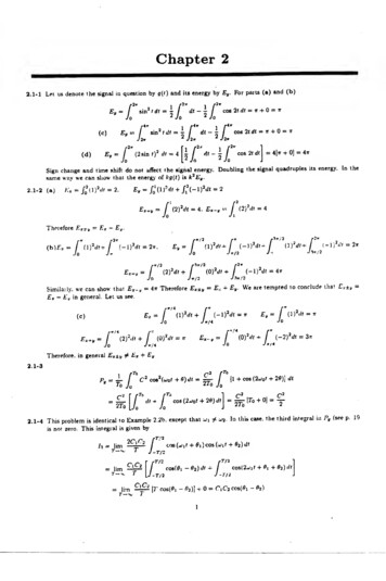
THE OP AMPOP AMP OPERATIONSECTION 1: OP AMP OPERATIONIntroductionThe op amp is one of the basic building blocks of linear design. In its classic form itconsists of two input terminals, one of which inverts the phase of the signal, the otherpreserves the phase, and an output terminal. The standard symbol for the op amp is givenin Figure 1.1. This ignores the power supply terminals, which are obviously required foroperation.( )INPUTS(-)Figure 1.1: Standard op amp symbolThe name “op amp” is the standard abbreviation for operational amplifier. This namecomes from the early days of amplifier design, when the op amp was used in analogcomputers. (Yes, the first computers were analog in nature, rather than digital). When thebasic amplifier was used with a few external components, various mathematical“operations” could be performed. One of the primary uses of analog computers wasduring WWII, when they were used for plotting ordinance trajectories.Voltage Feedback (VFB) ModelThe classic model of the voltage feedback op amp incorporates the followingcharacteristics:1.) Infinite input impedance2) Infinite bandwidth3) Infinite gain4) Zero output impedance5) Zero power consumption1.3
BASIC LINEAR DESIGNNone of these can be actually realized, of course. How close we come to these idealsdetermines the quality of the op amp.This is referred to as the voltage feedback model. This type of op amp comprises nearlyall op amps below 10 MHz bandwidth and on the order of 90% of those with higherbandwidths.POSITIVE SUPPLY( )INPUTSOP AMPOUTPUT(-)NEGATIVE SUPPLY IDEAL OP AMP ATTRIBUTES Infinite Differential GainZero Common Mode GainZero Offset VoltageZero Bias CurrentInfinite BandwidthOP AMP INPUT ATTRIBUTES Infinite ImpedanceZero Bias CurrentRespond to Differential VoltagesDo Not Respond to Common Mode VoltagesOP AMP OUTPUT ATTRIBITES Zero ImpedanceFigure 1.2: The Attributes of an Ideal Op AmpBasic OperationThe basic operation of the op amp can be easily summarized. First we assume that thereis a portion of the output that is fed back to the inverting terminal to establish the fixedgain for the amplifier. This is negative feedback. Any differential voltage across the input1.4
THE OP AMPOP AMP OPERATIONterminals of the op amp is multiplied by the amplifier’s open-loop gain. If the magnitudeof this differential voltage is more positive on the inverting (-) terminal than on thenoninverting ( ) terminal, the output will go more negative. If the magnitude of thedifferential voltage is more positive on the noninverting ( ) terminal than on the inverting(-) terminal, the output voltage will become more positive. The open-loop gain of theamplifier will attempt to force the differential voltage to zero. As long as the input andoutput stays in the operational range of the amplifier, it will keep the differential voltageat zero, and the output will be the input voltage multiplied by the gain set by thefeedback. Note from this that the inputs respond to differential mode not common-modeinput voltage.Inverting and Noninverting ConfigurationsThere are two basic ways to configure the voltage feedback op amp as an amplifier.These are shown in Figure 1.3 and Figure 1.4.Figure 1.3 shows what is known as the inverting configuration. With this circuit, theoutput is out of phase with the input. The gain of this circuit is determined by the ratio ofthe resistors used and is given by:A -Eq. 1-1R fbR inSUMMING POINTRGRFG VOUT/VIN - RF/RGVINOP AMPVOUTFigure 1.3: Inverting Mode Op Amp Stage1.5
BASIC LINEAR DESIGNFigure 1.4 shows what is know as the noninverting configuration. With this circuit theoutput is in phase with the input. The gain of the circuit is also determined by the ratio ofthe resistors used and is given by:A 1 R fbEq. 1-2R inOP AMPG VOUT/VIN 1 (RF/RG)RFVOUTVINRGFigure 1.4: Noninverting Mode Op Amp StageNote that since the output drives a voltage divider (the gain setting network) themaximum voltage available at the inverting terminal is the full output voltage, whichyields a minimum gain of 1.Also note that in both cases the feedback is from the output to the inverting terminal. Thisis negative feedback and has many advantages for the designer. These will be discussedmore in detail further in this chapter.It should also be noted that the gain is based on the ratio of the resistors, not their actualvalues. This means that the designer can choose just about any value he wishes withinpractical limits.If the values of the resistors are too low, a great deal of current would be required fromthe op amps output for operation. This causes excessive dissipation in the op amp itself,which has many disadvantages. The increased dissipation leads to self-heating of thechip, which could cause a change in the dc characteristics of the op amp itself. Also theheat generated by the dissipation could eventually cause the junction temperature to riseabove the 150 C, the commonly accepted maximum limit for most semiconductors. Thejunction temperature is the temperature at the silicon chip itself. On the other end of thespectrum, if the resistor values are too high, there is an increase in noise and the1.6
THE OP AMPOP AMP OPERATIONsusceptibility to parasitic capacitances, which could also limit bandwidth and possiblycause instability and oscillation.From a practical sense, resistors below 10 Ω and above 1 MΩ become increasinglydifficult to purchase especially if precision resistors are required.I1I2RGRFVINOP AMPVOUTFigure 1.5: Inverting Amplifier GainLet us look at the case of an inverting amp in a little more detail. Referring to Figure 1.5,the noninverting terminal is connected to ground. (We are assuming a bipolar ( and )power supply). Since the op amp will force the differential voltage across the inputs tozero, the inverting input will also appear to be at ground. In fact, this node is oftenreferred to as a “virtual ground.”If there is a voltage (Vin) applied to the input resistor, it will set up a current (I1) throughthe resistor (Rin) so thatI1 V inEq. 1.3R inSince the input impedance of the op amp is infinite, no current will flow into theinverting input. Therefore, this same current (I1) must flow through the feedback resistor(Rfb). Since the amplifier will force the inverting terminal to ground, the output willassume a voltage (Vout) such that:Vout I1 * R fbEq. 1-41.7
BASIC LINEAR DESIGNDoing a little simple arithmetic we then can come to the conclusion of eq. 1.1:Vo A VinRf bEq. 1-5R inG VOUTV INR FB 1 IVINVOUTRFBR INR INFigure 1.6: Noninverting Amplifier gainNow we examine the noninverting case in more detail. Referring to Figure 1.6, the inputvoltage is applied to the noninverting terminal. The output voltage drives a voltagedivider consisting of Rfb and Rin. The name “Rin,” in this instance, is somewhatmisleading since the resistor is not technically connected to the input, but we keep thesame designation since it matches the inverting configuration, has become a de factostandard, anyway. The voltage at the inverting terminal (Va), which is at the junction ofthe two resistors, isVa R inR in R fbVoEq. 1-6The negative feedback action of the op amp will force the differential voltage to 0 so:V a V inEq. 1-7Again applying a little simple arithmetic we end up with:VoVin R fb R inWhich is what we specified in Eq. 1-2.1.8R in 1 R fbR inEq. 1-8
THE OP AMPOP AMP OPERATIONIn all of the discussions above, we referred to the gain setting components as resistors. Infact, they are impedances, not just resistances. This allows us to build frequencydependent amplifiers. This will be covered in more detail in a later section.Open-Loop GainThe open-loop gain (usually referred to as AVOL) is the gain of the amplifier without thefeedback loop being closed, hence the name “open-loop.” For a precision op amp thisgain can be vary high, on the order of 160 dB or more. This is a gain of 100 million. Thisgain is flat from dc to what is referred to as the dominant pole. From there it falls off at6 dB/octave or 20 dB/decade. (An octave is a doubling in frequency and a decade is X10in frequency). This is referred to as a single-pole response. It will continue to fall at thisrate until it hits another pole in the response. This 2nd pole will double the rate at whichthe open-loop gain falls, that is, to 12 dB/octave or 40 dB/decade. If the open-loop gainhas dropped below 0 dB (unity gain) before it hits the 2nd pole, the op amp will beunconditional stable at any gain. This will be typically referred to as unity gain stable onthe data sheet. If the 2nd pole is reached while the loop gain is greater than 1 (0 dB), thenthe amplifier may not be stable under some dB/OCTAVE12dB/OCTAVEFigure 1.7: Open-Loop Gain (Bode Plot)It is important to understand the differences between open-loop gain, closed-loop gain,loop gain, signal gain, and noise gain. They are similar in nature, interrelated, butdifferent. We will discuss them all in detail.The open-loop gain is not a precisely controlled spec. It can, and does, have a relativelylarge range and will be given in the specs as a typical number rather than a min/maxnumber, in most cases. In some cases, typically high precision op amps, the spec will be aminimum.In addition, the open-loop gain can change due to output voltage levels and loading.There is also some dependency on temperature. In general, these effects are of a very1.9
BASIC LINEAR DESIGNminor degree and can, in most cases, be ignored. In fact this nonlinearity is not alwaysincluded in the data sheet for the part.GAINdBOPEN LOOP GAINLOOP GAINNOISE GAINCLOSED LOOP GAINLOG ffCLFigure 1.8: Gain DefinitionIN R1 AR1–R2INR1–R2C–R2INSignal Gain 1 R2/R1Signal Gain R2/R1Signal Gain - R2/R1Noise Gain 1 R2/R1Noise Gain 1 R2/R1Noise Gain 1 R2R1 R3 Voltage Noise and Offset Voltage of the op amp are reflected to theoutput by the Noise Gain. Noise Gain, not Signal Gain, is relevant in assessing stability. Circuit C has unchanged Signal Gain, but higher Noise Gain, thusbetter stability, worse noise, and higher output offset voltage.Figure 1.9: Noise Gain1.10 B
THE OP AMPOP AMP OPERATIONGain-Bandwidth ProductThe open-loop gain falls at 6 dB/octave. This means that if we double the frequency, thegain falls to half of what it was. Conversely, if the frequency is halved, the open-loopgain will double, as shown in Figure 1.8. This gives rise to what is known as the GainBandwidth Product. If we multiply the open-loop gain by the frequency the product isalways a constant. The caveat for this is that we have to be in the part of the curve that isfalling at 6 dB/octave. This gives us a convenient figure of merit with which to determineif a particular op amp is useable in a particular application.For example, if we have an application with which we require a gain of 10 and abandwidth of 100 kHz, we require an op amp with, at least, a gain-bandwidth product of1 MHz. This is a slight oversimplification. Because of the variability of the gainbandwidth product, and the fact that at the location where the closed-loop gain intersectsthe open-loop gain the response is actually down 3 dB, a little margin should be included.In the application described above, an op amp with a gain-bandwidth product of 1 MHzwould be marginal. A safety factor of at least 5 would be better insurance that theexpected performance is achieved.GAINdBOPEN LOOP GAIN, A(s)IF GAIN BANDWIDTH PRODUCT XTHEN Y · fCL XXYWHERE fCL CLOSED-LOOPBANDWIDTHfCL NOISE GAIN YY 1 R2R1fCLLOG fFigure 1.10: Gain-Bandwidth ProductStability CriteriaFeedback theory states that the closed-loop gain must intersect the open-loop gain at arate of 6 dB/octave (single-pole response) for the system to be stable. If the response is12 dB/octave (2 pole response) the op amp will oscillate. The easiest way to think of thisis that each pole adds 90 of phase shift. Two poles then means 180 , and 180 of phaseshift turns negative feedback into positive feedback, which means oscillations.1.11
BASIC LINEAR DESIGNThe question could be then, why would you want an amplifier that is not unity gainstable? The answer is that for a given amplifier, the bandwidth can be increased if theamplifier is not unity gain stable. This is sometimes referred to as decompensated, Butthe gain criteria must be met. This criteria is that the closed-loop gain must intercept theopen-loop gain at a slope of 6 dB/oct. (single-pole response). If not, the amplifierwill oscillate.As an example, compare the open-loop gain graphs in Figures 1.11, 1.12, 1.13. The threeparts shown, the AD847, AD848, and AD849, are basically the same part. The AD847 isunity gain stable. The AD848 is stable for gains of 2 or more. The AD849 is stable for again of 10 or more. You can see from this that the AD849 is much wider bandwidth. So,if you are going to run at high gain, you get wider bandwidth.There are a couple of tricks that you can use to help out in this regard in the circuit trickssection, which we will cover later.Figure 1.11: AD847 Open Loop GainFigure 1.12: AD848 Open Loop GainFigure 1.13: AD849 Open-Loop Gain1.12
THE OP AMPOP AMP OPERATIONPhase MarginOne measure of stability is phase margin. Just as the amplitude response doesn’t stay flatand then change instantaneously, the phase will also change gradually, starting as muchas a decade back from the corner frequency. Phase margin is the amount of phase shiftthat is left until you hit 180 measured at the unity gain point.The manifestation of low phase margin is an increase in the peaking of the output justbefore the close-loop gain intersects the open-loop gain. See Figure 1.14.80VS 5VRL 2kΩCL 5pF705040GAIN3018020135PHASE1045 PHASEMARGIN09045–100–2030k100k1M10MFREQUENCY (Hz)100MPHASE MARGIN (Degrees)OPEN-LOOP GAIN (dB)60500MFigure 1.14: AD8051 Phase MarginClosed-Loop GainThis, of course, is the gain of the amplifier with the feedback loop closed, as opposed theopen-loop gain, which is the gain with the feedback loop opened. It has two forms, signalgain and noise gain. These are described and differentiated below.The expression for the gain of a closed-loop amplifier involves the open-loop gain. If G isthe actual gain, NG is the noise gain (see below), and AVOL is the open-loop gain of theamplifier, then:G NG -NGN G2 NG ANG 1VOLA VOLEq. 1-9From this you can see that if the open-loop gain is very high, which it typically is, theclosed-loop gain of the circuit is simply the noise gain.1.13
BASIC LINEAR DESIGNSignal GainThis is the gain applied to the input signal, with the feedback loop connected. In the basicoperation section above, when we talked about the gain of the inverting and noninvertingcircuits, we were actually more correctly talking about the closed-loop signal gain. It canbe inverting or noninverting. It can even be less than unity for the inverting case. Signalgain is the gain that we are primarily interested in when designing circuits.The signal gain for an inverting amplifier stage is:A -R fbR inEq. 1-10and for a noninverting amplifier it is:A 1 R fbEq. 1-11R inNoise GainNoise gain is the gain applied to a noise source in series with an op amp input. It is alsothe gain applied to an offset voltage. The noise gain is equal to:A 1 R fbEq. 1-12R inNoise gain is equal to the signal gain of a noninverting amp. It is the same for either aninverting or noninverting stage.It is the noise gain that is used to determine stability. It is also the closed-loop gain that isused in Bode plots. Remember that even though we used resistances in the equation fornoise gain, they are actually impedances.1.14
THE OP AMPOP AMP OPERATIONIN R1 A BR1–R1–INR2C–R2INR2Signal Gain 1 R2/R1Signal Gain - R2/R1Signal Gain - R2/R1Noise Gain 1 R2/R1Noise Gain 1 R2/R1Noise Gain 1 R2R R3R1Voltage Noise and Offset Voltage of the op amp are reflected totheoutput by the Noise Gain. Noise Gain, not Signal Gain, is relevant in assessing stability. Circuit C has unchanged Signal Gain, but higher Noise Gain, thusbetter stability, worse noise, and higher output offset voltage.Figure 1.15: Noise GainLoop GainThe difference between the open-loop gain and the closed-loop gain is known as the loopgain. This is useful information because it gives you the amount of negative feedbackthat can apply to the amplifier system.GAINdBOPEN LOOP GAINCLOSED LOOP GAINLOOP GAINNOISE GAINfCLLOG fFigure 1.16: Gain Definitions1.15
BASIC LINEAR DESIGNBode PlotThe plotting of open-loop gain vs. frequency on a log-log scale gives is what is known asa Bode (pronounced boh dee) plot. It is one of the primary tools in evaluating whether aparticular op amp is suitable for a particular application.If you plot the open-loop gain and then the noise gain on a Bode plot, the point wherethey intersect will determine the maximum closed-loop bandwidth of the amplifiersystem. This is commonly referred to as the closed-loop frequency (FCL). Remember thatthe true response at the intersection is actually 3 dB down. One octave above and oneoctave below FCL the difference between the asymptotic response and the real responsewill be less than 1 dB.40GAIN3020NOISE GAINOPEN LOOP GAIN100FCLFREQUENCYFigure 1.17: Asymptotic ResponseThe Bode plot is also useful in determining stability. As stated above, if the closed-loopgain (noise gain) intersects the open-loop gain at a slope of greater than 6 dB/octave(20 dB/decade) the amplifier may be unstable (depending on the phase margin).1.16
THE OP AMPOP AMP OPERATIONCurrent Feedback (CFB) ModelThere is a type of amplifier that have several advantages over the standard VFB amplifierat high frequencies. They are called current feedback (CFB) or sometimestransimpedance amps. There is a possible point of confusion since the current–to-voltage(I/V) converters commonly found in photodiode applications are also referred to astransimpedance amps. Schematically CFB op amps look similar to standard VFB amps,but there are several key differences.The input structure of the CFB is different from the VFB. While we are trying not to getinto the internal structures of the op amps, in this case, a simple diagram is in order. SeeFigure 1.18. The mechanism of feedback is also different, hence the names. But again,the exact mechanism is beyond what we want to cover here. In most cases if thedifferences are noted, and the attendant limitations observed, the basic operation of bothtypes of amplifiers can be thought of as the same. The gain equations are the same as fora VFB amp, with an important limitation as noted in the next section.VIN –A(s) vv VIN–T(s) i 1VOUTii––R2R1A(s) OPEN LOOP GAINVOUT A(s)*vR1T(s) 1VOUTROR2T(s) TRANSIMPEDANCE OPEN LOOP GAINVOUT -T(s)*iFigure 1.18: VFB and CFB AmplifiersDifference from VFBOne primary difference between the CFB and VFB amps is that there is not a GainBandwidth product. While there is a change in bandwidth with gain, it is not even closeto the 6 dB/octave that we see with VFB. See Figure 1.19. Also, a major limitation thatthe value of the feedback resistor determines the bandwidth, working with the internalcapacitance of the op amp. For every CFB op amp there is a recommended value offeedback resistor for maximum bandwidth. If you increase the value of the resistor, youreduce the bandwidth. If you use a lower value of resistor the phase margin is reducedand the amplifier could become unstable. This optimum value of resistor is different fordifferent operational conditions. For instance, the value will change for differentpackages, for example, SOIC vs. DIP (see Figure 1.20).1.17
BASIC LINEAR DESIGNGAINdBG1G1 · f1G2 · f2G2f1 f2LOG f FEEDBACK RESISTOR FIXED FOR OPTIMUM PERFORMANCE. LARGER VALUESREDUCE BANDWIDTH, SMALLER VALUES MAY CAUSE INSTABILITY. FOR FIXED FEEDBACK RESISTOR, CHANGING GAIN HAS LITTLE EFFECT ONBANDWIDTH. CURRENT FEEDBACK OP AMPS DO NOT HAVE A FIXEDGAIN BANDWIDTHGAINPRODUCT.Figure 1.19: Current Feedback Amplifier Frequency ResponseAD8001AN (PDIP)GainAD8001ART (SOT-23-5)GainAD8001AR (SOIC)GainComponent–1 1 2 10 100–1 1 2 10 100–1 1 2 10 100RF (Ω)RG (Ω)RO (Nominal) (Ω)RS (Ω)RT (Nominal) (Ω)Small SignalBW (MHz)0.1 db 6049.92010570105130100120110300145Figure 1.20: AD8001 Optimum Feedback Resistor vs. PackageAlso, a CFB amplifier should not have a capacitor in the feedback loop. If a capacitor isused in the feedback loop, it reduces the feedback impedance as frequency is increased,which will cause the op amp to oscillate. You need to be careful of stray capacitancesaround the inverting input of the op amp for the same reason.A common error in using a current feedback op amp is to short the inverting inputdirectly to the output in an attempt to build a unity gain voltage follower (buffer). Thiscircuit will oscillate. Obviously, in this case, the feedback resistor value will be less therecommended value. The circuit is perfectly stable if the recommended feedback resistorof the correct value is used in place of the short.Another difference between the VFB and CFB amplifiers is that the inverting input of theCFB amp is low impedance. By low we mean typically 50 Ω to 100 Ω. Therefore thereisn’t the inherent balance between the inputs that the VFB circuit shows.1.18
THE OP AMPOP AMP OPERATIONSlew rate performance is also enhanced by the CFB topology. The current that isavailable to charge the internal compensation capacitor is dynamic. It is not limited toany fixed value as is often the case in VFB topologies. With a step input or overloadcondition, the current is increased (current-on-demand) until the overdriven condition isremoved. The basic current feedback amplifier has no fundamental slew-rate limit. Limitsonly come about from parasitic internal capacitances and many strides have been made toreduce their effects.The combination of higher bandwidths and slew rate allows CFB devices to have gooddistortion performance while doing so at a lower power.The distortion of an amplifier is impacted by the open loop distortion of the amplifier andthe loop gain of the closed-loop circuit. The amount of open-loop distortion contributedby a CFB amplifier is small due to the basic symmetry of the internal topology. Speed isthe other main contributor to distortion. In most configurations, a CFB amplifier has agreater bandwidth than its VFB counterpart. So at a given signal frequency, the faster parthas greater loop-gain and therefore lower distortion.How to Choose Between CFB and VFBThe application advantages of current feedback and voltage feedback differ. In manyapplications, the differences between CFB and VFB are not readily apparent. Today’sCFB and VFB amplifiers have comparable performance, but there are certain uniqueadvantages associated with each topology. Voltage feedback allows freedom of choice ofthe feedback resistor (or impedance) at the expense of sacrificing bandwidth for gain.Current feedback maintains high bandwidth over a wide range of gains at the cost oflimiting the choices in the feedback impedance.In general, VFB amplifiers offer: Lower Noise Better DC Performance Feedback Component Freedomwhile CFB amplifiers offer: Faster Slew Rates Lower Distortion Feedback Component RestrictionsSupply VoltagesHistorically the supply voltage for op amps was typically 15 V. The operational inputand output range was on the order of 10 V. But there was no hard requirement for theselevels. Typically the maximum supply was 18 V. The lower limit was set by the internalstructures. You could typically go within 1.5 or 2 V of either supply rail, so you couldreasonably go down to 8 V supplies or so and still have a reasonable dynamic range.1.19
BASIC LINEAR DESIGNLately though, there has been a trend toward lower supply voltages. This has happenedfor a couple of reasons.First, high speed circuits typically have a lower full scale range. The principal reason forthis is the amplifiers ability to swing large voltages. All amplifiers have a slew rate limit,which is expressed as so many volts per microsecond. So if you want to go faster, yourvoltage range must be reduced, all other things being equal. A second reason is that tolimit the effects of stray capacitance on the circuits, you need to reduce their impedancelevels. Driving lower impedances increases the demands on the output stage, and on thepower dissipation abilities of the amplifier package. Lower voltage swings require lowercurrents to be supplied, thereby lowering the dissipation of the package.A second reason is that as the speed of the devices inside the amplifier increased, thegeometries of these devices tend to become smaller. The smaller geometries typicallymean reduced breakdown voltages for these parts. Since the breakdown voltages weregetting lower, the supply voltages had to follow. Today high speed op amps typicallyhave breakdown voltage of 7 V, and so the supplies are typically 5 V, or even lower.In some cases, operation on batteries established a requirement for lower supply voltages.Lower supplies would then lessen the number of batteries, which, in turn, reduced thesize, weight and cost of the end product.At the same time there was a movement towards single supply systems. Instead of thetypical plus and minus supplies, the op amps operate on a single positive supply andground, the ground then becoming the negative supply.Single Supply ConsiderationsThere is nothing in the circuitry of the op amp that requires ground. In fact, instead of abipolar ( and ) supply of 15 V you could just as easily use a single supply of 30 V(ground being the negative supply), as long as the rest of the circuit was biased correctlyso that the signal was within the common mode range of op amp. Or, for that matter, thesupply could just as easily be –30 V (ground being the most positive supply).When you combine the single supply operation with reduced supply voltages you can runinto problems. The standard topology for op amps uses a NPN di
BASIC LINEAR DESIGN 1.4 None of these can be actually realized, of course. How close we come to these ideals determines the quality of the op amp. This is referred to as the voltage feedback model. This type of op amp comprises nearly all op amps below 10 MHz bandwidth