Transcription
MT-087TUTORIALVoltage ReferencesINTRODUCTIONVoltage references and linear regulators have much in common. In fact, the latter could befunctionally described as a reference circuit, but with greater current (or power) output.Accordingly, almost all of the specifications of the two circuit types have great commonality(even though the performance of references is usually tighter with regard to drift, accuracy, etc.).In many cases today the support circuitry is included in the converter package. This isadvantageous to the designer since it simplifies the design process and guarantees performanceof the system.Voltage references have a major impact on the performance and accuracy of analog systems. A 5 mV tolerance on a 5 V reference corresponds to 0.1% absolute accuracy which is only 10bit accuracy. For a 12-bit system, choosing a reference that has a 1 mV tolerance may be farmore cost effective than performing manual calibration, while both high initial accuracy andcalibration will be necessary in a system making absolute 16-bit measurements. Note that manysystems make relative measurements rather than absolute ones, and in such cases the absoluteaccuracy of the reference is not as important, although noise and short-term stability may be.Temperature drift or drift due to aging may be an even greater problem than absolute accuracy.The initial error can always be trimmed, but compensating for drift is difficult. Where possible,references should be chosen for temperature coefficient and aging characteristics which preserveadequate accuracy over the operating temperature range and expected lifetime of the system.Noise in voltage references is often overlooked, but it can be very important in system design.Noise is an instantaneous change in the reference voltage. It is generally specified on data sheets,but system designers frequently ignore the specification and assume that voltage references donot contribute to system noise.There are two dynamic issues that must be considered with voltage references: their behavior atstart-up, and their behavior with transient loads. With regard to the first, always bear in mind thatvoltage references do not power up instantly (this is true of references inside ADCs and DACs aswell as discrete designs). Thus it is rarely possible to turn on an ADC and reference, whetherinternal or external, make a reading, and turn off again within a few microseconds, howeverattractive such a procedure might be in terms of energy saving.Regarding the second point, a given reference IC may or may not be well suited for pulseloading conditions, dependent upon the specific architecture. Many references use low power,and therefore low bandwidth, output buffer amplifiers. This makes for poor behavior under fasttransient loads, which may degrade the performance of fast ADCs (especially successiveapproximation and flash ADCs). Suitable decoupling can ease the problem (but some referencesoscillate with capacitive loads), or an additional external broadband buffer amplifier may be usedto drive the node where the transients occur.Rev.0, 10/08, WKPage 1 of 18
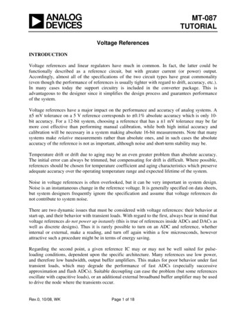
MT-087SIMPLE DIODE REFERENCESIn terms of the functionality of their circuit connection, standard reference ICs are often onlyavailable in series, or three-terminal form (VIN, Common, VOUT), and also in positive polarityonly. The series types have the potential advantages of lower and more stable quiescent current,standard pre-trimmed output voltages, and relatively high output current without accuracy loss.Shunt, or two-terminal (i.e., diode-like) references are more flexible regarding operating polarity,but they are also more restrictive as to loading. They can in fact eat up excessive power withwidely varying resistor-fed voltage inputs. Also, they sometimes come in non-standard voltages.All of these various factors tend to govern when one functional type is preferred over the other.Some simple diode-based references are shown in Figure 1. In the first of these, a current drivenforward biased diode (or diode-connected transistor) produces a voltage, Vf VREF. While thejunction drop is somewhat decoupled from the raw supply, it has numerous deficiencies as areference. Among them are a strong TC of about –0.3%/ C, some sensitivity to loading, and arather inflexible output voltage, it is only available in 600 mV jumps. VSRS VSIDRZIZD1D1VREFVREFD2FORWARD-BIASEDDIODEZENER (AVALANCHE)DIODEFigure 1: Simple Diode Reference CircuitsBy contrast, these most simple references (as well as all other shunt-type regulators) have a basicadvantage, which is the fact that the polarity is readily reversible by flipping connections andreversing the drive current. However, a basic limitation of all shunt regulators is that load currentmust always be less (usually appreciably less) than the driving current, ID.In the second circuit of Figure 1, a zener or avalanche diode is used, and an appreciably higheroutput voltage realized. While true zener breakdown occurs below 5 V, avalanche breakdownoccurs at higher voltages and has a positive temperature coefficient. Note that diode reversebreakdown is referred to almost universally today as zener, even though it is usually avalanchebreakdown. With a D1 breakdown voltage in the 5 to 8 V range, the net positive TC is such thatPage 2 of 18
MT-087it equals the negative TC of forward-biased diode D2, yielding a net TC of 100 ppm/ C or lesswith proper bias current. Combinations of such carefully chosen diodes formed the basis of theearly single package "temperature-compensated zener" references, such as the 1N821-1N829series.The temperature-compensated zener reference is limited in terms of initial accuracy, since thebest TC combinations fall at odd voltages, such as the 1N829's 6.2 V. And, the scheme is alsolimited for loading, since for best TC the diode current must be carefully controlled. Unlike afundamentally lower voltage ( 2 V) reference, zener diode based references must of necessity bedriven from voltage sources appreciably higher than 6 V levels, so this precludes operation ofzener references from 5 V system supplies. References based on low TC zener (avalanche)diodes also tend to be noisy, due to the basic noise of the breakdown mechanism. This has beenimproved greatly with monolithic zener types, as is described further below.BANDGAP REFERENCESThe development of low voltage ( 5 V) references based on the bandgap voltage of silicon led tothe introductions of various ICs which could be operated on low voltage supplies with good TCperformance. The first of these was the LM109 (Reference 1), and a basic bandgap reference cellis shown in Figure 2. VSIZR2 ΔVBER3R26kΩR1600ΩVR VBE Q2R2 ΔVBER3Q3Q1R3600ΩΔVBEVBEFigure 2: Basic Bandgap ReferenceThis circuit is also called a "ΔVBE" reference because the differing current densities betweenmatched transistors Q1-Q2 produces a ΔVBE across R3. It works by summing the VBE of Q3 withthe amplified ΔVBE of Q1-Q2, developed across R2. The ΔVBE and VBE components haveopposite polarity TCs; ΔVBE is proportional-to-absolute-temperature (PTAT), while VBE isPage 3 of 18
MT-087complementary-to-absolute-temperature (CTAT). The summed output is VR, and when it is equalto 1.205 V (silicon bandgap voltage), the TC is a minimum.The bandgap reference technique is attractive in IC designs because of several reasons; amongthese are the relative simplicity, and the avoidance of zeners and their noise. However, veryimportant in these days of ever decreasing system supplies is the fundamental fact that bandgapdevices operate at low voltages, i.e., 5 V. Not only are they used for stand-alone IC references,but they are also used within the designs of many other linear ICs such as ADCs and DACs.However, the basic designs of Figure 2 suffer from load and current drive sensitivity, plus thefact that the output needs accurate scaling to more useful levels, i.e., 2.5 V, 5 V, etc. The loaddrive issue is best addressed with the use of a buffer amplifier, which also provides convenientvoltage scaling to standard levels.An improved three-terminal bandgap reference, the AD580 (introduced in 1974) is shown inFigure 3. Popularly called the "Brokaw Cell" (see References 2 and 3), this circuit provides onchip output buffering, which allows good drive capability and standard output voltage scaling. VINR8R7 I2 I1VOUT 2.5VR4Q28AΔVBEQ1VZ 1.205VAVBE(Q1)R2R5A TRANSISTORAREAR1V1 2R1 ΔVBER2COMFigure 3: AD580 Precision Bandgap Reference Uses Brokaw Cell (1974)The AD580 was the first precision bandgap based IC reference, and variants of the topologyhave influenced further generations of both industry standard references such as the REF01,REF02, and REF03 series, as well as more recent ADI bandgap parts such as the REF19x series,the AD680, AD780, the AD1582-85 series, the ADR38x series, the ADR39x series, and recentSC-70 and SOT-23 offerings of improved versions of the REF01, REF02, and REF03(designated ADR01, ADR02, and ADR03).The AD580 has two 8:1 emitter-scaled transistors Q1-Q2 operating at identical collector currents(and thus 1/8 current densities), by virtue of equal load resistors and a closed loop around thePage 4 of 18
MT-087buffer op amp. Due to the resultant smaller VBE of the 8 area Q2, R2 in series with Q2 drops theΔVBE voltage, while R1 (due to the current relationships) drops a PTAT voltage V1:V1 2 R1 ΔVBE .R2Eq. 1The bandgap cell reference voltage VZ appears at the base of Q1, and is the sum of VBE (Q1) andV1, or 1.205 V, the bandgap voltage:VZ VBE(Q1) V1R1 ΔVBER2R1 kTJ1 VBE(Q1) 2 lnR2 qJ2R1 kT VBE(Q1) 2 ln8R2 q 1.205V . VBE(Q1) 2 Eq. 2Eq. 3Eq. 4Eq. 5Note that J1 current density in Q1, J2 current density in Q2, and J1/J2 8.However, because of the presence of the R4/R5 (laser trimmed) thin film divider and the op amp,the actual voltage appearing at VOUT can be scaled higher, in the AD580 case 2.5 V. Followingthis general principle, VOUT can be raised to other practical levels, such as for example in theAD584, with taps for precise 2.5, 5, 7.5, and 10 V operation. The AD580 provides up to 10-mAoutput current while operating from supplies between 4.5 and 30 V. It is available in tolerancesas low as 0.4%, with TCs as low as 10 ppm/ C.Many of the recent developments in bandgap references have focused on smaller package sizeand cost reduction, to address system needs for smaller, more power efficient and less costlyreference ICs. Among these are several recent bandgap-based IC references. The AD1580(introduced in 1996) is a shunt mode IC reference which is functionally quite similar to theclassic shunt IC reference, the AD589 (introduced in 1980) mentioned above. A key difference isthe fact that the AD1580 uses a newer, small geometry process, enabling its availability withinthe tiny SOT-23 package. The very small size of this package allows use in a wide variety ofspace limited applications, and the low operating current lends itself to portable battery powereduses. The AD1580 circuit is shown in simplified form in Figure 4.In this circuit, like transistors Q1 and Q2 form the bandgap core, and are operated at a currentratio of 5 times, determined by the ratio of R7 to R2. An op amp is formed by the differentialpair Q3-Q4, current mirror Q5, and driver/output stage Q8-Q9. In closed loop equilibrium, thisamplifier maintains the bottom ends of R2-R7 at the same potential.Page 5 of 18
MT-087V R5R6R1Q5V1Q8R2–R7Q9Q3 Q4R3ΔVBEQ2–Q1 R4V–VBE–Figure 4: AD1580 1.2V Shunt Type Bandgap Referencehas Tiny Size in SOT-23 FootprintAs a result of the closed loop control described, a basic ΔVBE voltage is dropped across R3, and ascaled PTAT voltage also appears as V1, which is effectively in series with VBE. The nominalbandgap reference voltage of 1.225 V is then the sum of Q1's VBE and V1. The AD1580 isdesigned to operate at currents as low as 50 µA, also handling maximum currents as high as 10mA. It is available in grades with voltage tolerances of 1 or 10 mV, and with correspondingTCs of 50 or 100 ppm/ C. Newer members of the Analog Devices' family of shunt regulators arethe ADR510 (1.000 V), and the ADR512 (1.200 V).The ADR520 (2.048 V), ADR525 (2.500 V), ADR530 (3.000 V), ADR540 (4.096 V), ADR545(4.5 V), and ADR550 (5.0 V) are the latest in the shunt regulator family, with initial accuraciesof 0.2%, and available in either SC-70 or SOT-23 packages.The AD1582-AD1585 series comprises a family of series mode IC references, which producevoltage outputs of 2.5, 3.0, 4.096 and 5.0 V. Like the AD1580, the series uses a small geometryprocess to allow packaging within an SOT-23.The circuit diagram for the AD1582-AD1585 series, shown in Figure 5, may be recognized as avariant of the basic Brokaw bandgap cell, as described under Figure 3. In this case Q1-Q2 formthe core, and the overall loop operates to produce the stable reference voltage VBG at the base ofQ1. A notable difference here is that the op amp's output stage is designed with push-pullcommon-emitter stages. This has the effect of requiring an output capacitor for stability, but italso provides the IC with relatively low dropout operation.Page 6 of 18
MT-087VINR3R4VOUT R5Q1Q2ΔVBEVBGR6R2R1V1 2R1 ΔVBER2GNDFigure 5: AD1582-AD1585 2.5-5V Series Type Bandgap References1VIN3 COUTVOUT1 µF24.7 µFAD1582-1585: COUT REQUIRED FOR STABILITYADR380, ADR381: COUT RECOMMENDED TO ABSORB TRANSIENTSFigure 6: AD1582-AD1585 Series Connection DiagramThe low dropout feature means essentially that VIN can be lowered to as close as several hundredmV above the VOUT level without disturbing operation. The push-pull operation also means thatthis device series can actually both sink and source currents at the output, as opposed to theclassic reference operation of sourcing current (only). For the various output voltage ratings, thedivider R5-R6 is adjusted for the respective levels.Page 7 of 18
MT-087The AD1582-series is designed to operate with quie
Some simple diode-based references are shown in Figure 1. In the first of these, a current driven forward biased diode (or diode-connected transistor) produces a voltage, Vf VREF. While the junction drop is somewhat decoupled from the raw supply, it has numerous deficiencies as a reference. Among them are a strong TC of about –0.3%/ C, some sensitivity to loading, and aFile Size: 229KBPage Count: 18