Transcription
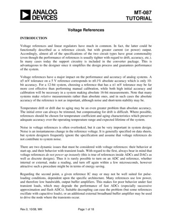
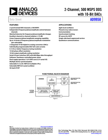
2-Channel, 500 MSPS DDSwith 10-Bit DACsAD9958Data SheetFEATURESAPPLICATIONS2 synchronized DDS channels @ 500 MSPSIndependent frequency/phase/amplitude control betweenchannelsMatched latencies for frequency/phase/amplitude changesExcellent channel-to-channel isolation ( 72 dB)Linear frequency/phase/amplitude sweeping capabilityUp to 16 levels of frequency/phase/amplitude modulation(pin-selectable)2 integrated 10-bit digital-to-analog converters (DACs)Individually programmable DAC full-scale currents0.12 Hz or better frequency tuning resolution14-bit phase offset resolution10-bit output amplitude scaling resolutionSerial I/O port interface (SPI) with 800 Mbps data throughputSoftware-/hardware-controlled power-downDual supply operation (1.8 V DDS core/3.3 V serial I/O)Multiple device synchronizationSelectable 4 to 20 REFCLK multiplier (PLL)Selectable REFCLK crystal oscillator56-lead LFCSPAgile local oscillatorsPhased array radars/sonarsInstrumentationSynchronized clockingRF source for AOTFSingle-side band suppressed carriersQuadrature communicationsFUNCTIONAL BLOCK DIAGRAMAD9958(2)500MSPSDDS CORES10-BITDACRECONSTRUCTEDSINE WAVE10-BITDACRECONSTRUCTEDSINE WAVEMODULATION CONTROLREF CLOCKINPUT CIRCUITRYTIMING ANDCONTROLUSER INTERFACE05252-000SYSTEMCLOCKSOURCEFigure 1.Rev. CDocument FeedbackInformation furnished by Analog Devices is believed to be accurate and reliable. However, noresponsibility is assumed by Analog Devices for its use, nor for any infringements of patents or otherrights of third parties that may result from its use. Specifications subject to change without notice. Nolicense is granted by implication or otherwise under any patent or patent rights of Analog Devices.Trademarks and registered trademarks are the property of their respective owners.One Technology Way, P.O. Box 9106, Norwood, MA 02062-9106, U.S.A.Tel: 781.329.4700 2005–2016 Analog Devices, Inc. All rights reserved.Technical Supportwww.analog.com
AD9958Data SheetTABLE OF CONTENTSFeatures . 1Applications . 1Functional Block Diagram . 1Revision History . 2General Description . 3Specifications. 4Absolute Maximum Ratings . 8ESD Caution . 8Pin Configuration and Function Descriptions . 9Typical Performance Characteristics . 11Application Circuits . 14Equivalent Input and Output Circuits . 17Theory of Operation . 18DDS Core. 18Digital-to-Analog Converter . 18Modes of Operation . 19Channel Constraint Guidelines . 19Power Supplies . 19Single-Tone Mode . 19Reference Clock Modes . 20Scalable DAC Reference Current Control Mode . 21Power-Down Functions . 21Modulation Mode. 21Modulation Using SDIO x Pins for RU/RD . 24Linear Sweep Mode . 25Linear Sweep No-Dwell Mode . 26Sweep and Phase Accumulator Clearing Functions . 27Output Amplitude Control Mode . 28Synchronizing Multiple AD9958 Devices . 29Automatic Mode Synchronization . 29Manual Software Mode Synchronization . 29Manual Hardware Mode Synchronization . 29I/O UPDATE, SYNC CLK, and System ClockRelationships . 30Serial I/O Port . 31Overview . 31Instruction Byte Description . 32Serial I/O Port Pin Description . 32Serial I/O Port Function Description . 32MSB/LSB Transfer Description . 32Serial I/O Modes of Operation . 33Register Maps and Bit Descriptions . 36Register Maps . 36Descriptions for Control Registers . 39Descriptions for Channel Registers . 41Outline Dimensions . 44Ordering Guide . 44REVISION HISTORY11/2016—Rev. B to Rev. CChange to Figure 37 Caption . 264/2013—Rev. A to Rev. BChanges to Linear Sweep Mode Section and Setting the Slope ofthe Linear Sweep . 25Changes to Figure 38 and Figure 39 Captions . 27Changes to Ramp Rate Timer Section . 28Updated Outline Dimensions . 447/2008—Rev. 0 to Rev. AChanges to Features. 1Inserted Figure 1; Renumbered Sequentially . 1Changes to Input Level Parameter in Table 1 . 4Added Profile Pin Toggle Rate Parameter in Table 1 . 6Changes to Layout . 8Changes to Table 3 . 9Added Equivalent Input and Output Circuits Section . 17Changes to Reference Clock Input Circuitry Section . 20Change to Figure 35 . 21Changes to Setting the Slope of the Linear Sweep Section . 25Changes to Figure 37. 26Changes to Figure 38 and Figure 39 . 27Changes to Figure 40. 30Added Table 25; Renumbered Sequentially . 31Changes to Figure 41. 31Changes to Figure 42, Serial Data I/O (SDIO 0, SDIO 1,SDIO 3) Section, and Added Example Instruction ByteSection . 32Added Table 27 . 33Changes to Figure 46, Figure 47, Figure 48, and Figure 49 . 35Changes to Register Maps and Bit Descriptions Section andAdded Endnote 2 to Table 28. 36Added Endnote 1 to Table 30. 38Added Exposed Pad Notation to Outline Dimensions . 449/2005—Revision 0: Initial VersionRev. C Page 2 of 44
Data SheetAD9958GENERAL DESCRIPTIONThe DAC outputs are supply referenced and must be terminated into AVDD by a resistor or an AVDD center-tappedtransformer. Each DAC has its own programmable reference toenable different full-scale currents for each channel.The AD9958 consists of two DDS cores that provide independent frequency, phase, and amplitude control on each channel.This flexibility can be used to correct imbalances betweensignals due to analog processing, such as filtering, amplification,or PCB layout related mismatches. Because both channels sharea common system clock, they are inherently synchronized.Synchronization of multiple devices is supported.The DDS acts as a high resolution frequency divider with theREFCLK as the input and the DAC providing the output. TheREFCLK input source is common to both channels and can bedriven directly or used in combination with an integratedREFCLK multiplier (PLL) up to a maximum of 500 MSPS. ThePLL multiplication factor is programmable from 4 to 20, ininteger steps. The REFCLK input also features an oscillatorcircuit to support an external crystal as the REFCLK source.The crystal must be between 20 MHz and 30 MHz. The crystalcan be used in combination with the REFCLK multiplier.The AD9958 can perform up to a 16-level modulation offrequency, phase, or amplitude (FSK, PSK, ASK). Modulation isperformed by applying data to the profile pins. In addition, theAD9958 also supports linear sweep of frequency, phase, oramplitude for applications such as radar and instrumentation.The AD9958 serial I/O port offers multiple configurations toprovide significant flexibility. The serial I/O port offers an SPIcompatible mode of operation that is virtually identical to theSPI operation found in earlier Analog Devices, Inc., DDSproducts. Flexibility is provided by four data pins (SDIO 0/SDIO 1/SDIO 2/SDIO 3) that allow four programmablemodes of serial I/O operation.The AD9958 comes in a space-saving 56-lead LFCSP package.The DDS core (AVDD and DVDD pins) is powered by a 1.8 Vsupply. The digital I/O interface (SPI) operates at 3.3 V andrequires the pin labeled DVDD I/O (Pin 49) be connectedto 3.3 V.The AD9958 operates over the industrial temperature range of 40 C to 85 C.The AD9958 uses advanced DDS technology that provides lowpower dissipation with high performance. The device incorporatestwo integrated, high speed 10-bit DACs with excellent widebandand narrow-band SFDR. Each channel has a dedicated 32-bitfrequency tuning word, 14 bits of phase offset, and a 10-bitoutput scale multiplier.AD9958DDS COREΣ3232ΣΣ15COS(X)1010DAC1010DACCH0 IOUTCH0 IOUTDDS CORE32FTW FTW3232SYNC INSYNC OUTI/O UPDATESYNC CLKΣPHASE/ PHASE15COS(X)14AMP/ AMPSCALABLEDAC REFCURRENT10TIMING AND CONTROL LOGICSYSTEMCLK 4REF CLKREF CLKΣBUFFER/XTALOSCILLATORCLK MODE SELREF CLOCKMULTIPLIER4 TO 20 CH1 IOUTCH1 IOUTDAC RSETPWR DWN CTLMASTER ERSPROFILEREGISTERS1.8V1.8VAVDDDVDDFigure 2. Detailed Block DiagramRev. C Page 3 of 44P0 P1P2P3DVDD I/OSCLKCSSDIO 0SDIO 1SDIO 2SDIO 305252-001Σ
AD9958Data SheetSPECIFICATIONSAVDD and DVDD 1.8 V 5%; DVDD I/O 3.3 V 5%; T 25 C; RSET 1.91 kΩ; external reference clock frequency 500 MSPS(REFCLK multiplier bypassed), unless otherwise noted.Table 1.ParameterREFERENCE CLOCK INPUT CHARACTERISTICSFrequency RangeREFCLK Multiplier BypassedREFCLK Multiplier EnabledInternal VCO Output Frequency RangeVCO Gain Control Bit Set High 1VCO Gain Control Bit Set Low1Crystal REFCLK Source RangeInput LevelInput Voltage Bias LevelInput CapacitanceInput ImpedanceDuty Cycle with REFCLK Multiplier BypassedDuty Cycle with REFCLK Multiplier EnabledCLK Mode Select (Pin 24) Logic 1 VoltageCLK Mode Select (Pin 24) Logic 0 VoltageDAC OUTPUT CHARACTERISTICSResolutionFull-Scale Output CurrentGain ErrorChannel-to-Channel Output Amplitude Matching ErrorOutput Current OffsetDifferential NonlinearityIntegral NonlinearityOutput CapacitanceVoltage Compliance RangeChannel-to-Channel IsolationWIDEBAND SFDR1 MHz to 20 MHz Analog Output20 MHz to 60 MHz Analog Output60 MHz to 100 MHz Analog Output100 MHz to 150 MHz Analog Output150 MHz to 200 MHz Analog OutputNARROW-BAND SFDR1.1 MHz Analog Output ( 10 kHz)1.1 MHz Analog Output ( 50 kHz)1.1 MHz Analog Output ( 250 kHz)1.1 MHz Analog Output ( 1 MHz)15.1 MHz Analog Output ( 10 kHz)15.1 MHz Analog Output ( 50 kHz)15.1 MHz Analog Output ( 250 kHz)15.1 MHz Analog Output ( 1 MHz)40.1 MHz Analog Output ( 10 kHz)40.1 MHz Analog Output ( 50 kHz)40.1 MHz Analog Output ( 250 kHz)40.1 MHz Analog Output ( 1 MHz)75.1 MHz Analog Output ( 10 0.51.25 10 2.51 0.5 1.03AVDD 0.50721010 10 2.525AVDD 0.50Measured at each pin (single-ended)1.8 V digital input logic1.8 V digital input logicMust be referenced to AVDDBitsmA% FS%µALSBLSBpFVdB 65 62 59 56 53dBcdBcdBcdBcdBc 90 88 86 85 90 87 85 83 90 87 84 82 87dBcdBcdBcdBcdBcdBcdBcdBcdBcdBcdBcdBcdBcRev. C Page 4 of 44Test Conditions/CommentsSee Figure 34 and Figure 35DAC supplies tied together (see Figure 19)The frequency range for wideband SFDRis defined as dc to Nyquist
Data SheetParameter75.1 MHz Analog Output ( 50 kHz)75.1 MHz Analog Output ( 250 kHz)75.1 MHz Analog Output ( 1 MHz)100.3 MHz Analog Output ( 10 kHz)100.3 MHz Analog Output ( 50 kHz)100.3 MHz Analog Output ( 250 kHz)100.3 MHz Analog Output ( 1 MHz)200.3 MHz Analog Output ( 10 kHz)200.3 MHz Analog Output ( 50 kHz)200.3 MHz Analog Output ( 250 kHz)200.3 MHz Analog Output ( 1 MHz)PHASE NOISE CHARACTERISTICSResidual Phase Noise @ 15.1 MHz (fOUT)@ 1 kHz Offset@ 10 kHz Offset@ 100 kHz Offset@ 1 MHz OffsetResidual Phase Noise @ 40.1 MHz (fOUT)@ 1 kHz Offset@ 10 kHz Offset@ 100 kHz Offset@ 1 MHz OffsetResidual Phase Noise @ 75.1 MHz (fOUT)@ 1 kHz Offset@ 10 kHz Offset@ 100 kHz Offset@ 1 MHz OffsetResidual Phase Noise @ 100.3 MHz (fOUT)@ 1 kHz Offset@ 10 kHz Offset@ 100 kHz Offset@ 1 MHz OffsetResidual Phase Noise @ 15.1 MHz (fOUT) with REFCLKMultiplier Enabled 5 @ 1 kHz Offset@ 10 kHz Offset@ 100 kHz Offset@ 1 MHz OffsetResidual Phase Noise @ 40.1 MHz (fOUT) with REFCLKMultiplier Enabled 5 @ 1 kHz Offset@ 10 kHz Offset@ 100 kHz Offset@ 1 MHz OffsetResidual Phase Noise @ 75.1 MHz (fOUT) with REFCLKMultiplier Enabled 5 @ 1 kHz Offset@ 10 kHz Offset@ 100 kHz Offset@ 1 MHz OffsetResidual Phase Noise @ 100.3 MHz (fOUT) with REFCLKMultiplier Enabled 5 @ 1 kHz Offset@ 10 kHz Offset@ 100 kHz Offset@ 1 MHz OffsetAD9958MinTyp 85 83 82 87 85 83 81 87 85 83 81MaxUnitdBcdBcdBcdBcdBcdBcdBcdBcdBcdBcdBc 150 159 165 165dBc/HzdBc/HzdBc/HzdBc/Hz 142 151 160 162dBc/HzdBc/HzdBc/HzdBc/Hz 135 146 154 157dBc/HzdBc/HzdBc/HzdBc/Hz 134 144 152 154dBc/HzdBc/HzdBc/HzdBc/Hz 139 149 153 148dBc/HzdBc/HzdBc/HzdBc/Hz 130 140 145 139dBc/HzdBc/HzdBc/HzdBc/Hz 123 134 138 132dBc/HzdBc/HzdBc/HzdBc/Hz 120 130 135 129dBc/HzdBc/HzdBc/HzdBc/HzRev. C Page 5 of 44Test Conditions/Comments
AD9958ParameterResidual Phase Noise @ 15.1 MHz (fOUT) with REFCLKMultiplier Enabled 20 @ 1 kHz Offset@ 10 kHz Offset@ 100 kHz Offset@ 1 MHz OffsetResidual Phase Noise @ 40.1 MHz (fOUT) with REFCLKMultiplier Enabled 20 @ 1 kHz Offset@ 10 kHz Offset@ 100 kHz Offset@ 1 MHz OffsetResidual Phase Noise @ 75.1 MHz (fOUT) with REFCLKMultiplier Enabled 20 @ 1 kHz Offset@ 10 kHz Offset@ 100 kHz Offset@ 1 MHz OffsetResidual Phase Noise @ 100.3 MHz (fOUT) with REFCLKMultiplier Enabled 20 @ 1 kHz Offset@ 10 kHz Offset@ 100 kHz Offset@ 1 MHz OffsetSERIAL PORT TIMING CHARACTERISTICSMaximum Frequency Serial Clock (SCLK)Minimum SCLK Pulse Width Low (tPWL)Minimum SCLK Pulse Width High (tPWH)Minimum Data Setup Time (tDS)Minimum Data Hold TimeMinimum CS Setup Time (tPRE)Minimum Data Valid Time for Read OperationMISCELLANEOUS TIMING CHARACTERISTICSMASTER RESET Minimum Pulse WidthI/O UPDATE Minimum Pulse WidthMinimum Setup Time (I/O UPDATE to SYNC CLK)Minimum Hold Time (I/O UPDATE to SYNC CLK)Minimum Setup Time (Profile Inputs to SYNC CLK)Minimum Hold Time (Profile Inputs to SYNC CLK)Minimum Setup Time (SDIO Inputs to SYNC CLK)Minimum Hold Time (SDIO Inputs to SYNC CLK)Propagation Time Between REF CLK and SYNC CLKProfile Pin Toggle RateCMOS LOGIC INPUTSVIHVILLogic 1 CurrentLogic 0 CurrentInput CapacitanceCMOS LOGIC OUTPUTSVOHVOLData SheetMinTypMax 127 136 139 138dBc/HzdBc/HzdBc/HzdBc/Hz 117 128 132 130dBc/HzdBc/HzdBc/HzdBc/Hz 110 121 125 123dBc/HzdBc/HzdBc/HzdBc/Hz 107 119 121 05.402.502.25Unit3.55.522.03 1220.812Test ncclocksMin pulse width 1 sync clock periodMin pulse width 1 sync clock periodRising edge to rising edgeRising edge to rising edgeVVµAµApF1 mA load2.70.4Rev. C Page 6 of 44VV
Data SheetParameterPOWER SUPPLYTotal Power Dissipation—Both Channels On, SingleTone ModeTotal Power Dissipation—Both Channels On, withSweep AccumulatorTotal Power Dissipation—Full Power-DownIAVDD—Both Channels On, Single-Tone ModeIAVDD—Both Channels On, Sweep Accumulator,REFCLK Multiplier, and 10-Bit Output ScalarEnabledIDVDD—Both Channels On, Single-Tone ModeIDVDD—Both Channels On, Sweep Accumulator,REFCLK Multiplier, and 10-Bit Output ScalarEnabledIDVDD I/OIAVDD Power-Down ModeIDVDD Power-Down ModeDATA LATENCY (PIPELINE DELAY) SINGLE-TONE MODE 2, 3Frequency, Phase, and Amplitude Words to DACOutput with Matched Latency EnabledFrequency Word to DAC Output with MatchedLatency DisabledPhase Offset Word to DAC Output with MatchedLatency DisabledAmplitude Word to DAC Output with MatchedLatency DisabledDATA LATENCY (PIPELINE DELAY) MODULATION MODE3, 4Frequency Word to DAC OutputPhase Offset Word to DAC OutputAmplitude Word to DAC OutputDATA LATENCY (PIPELINE DELAY) LINEAR SWEEP MODE3, 4Frequency Rising/Falling Delta-Tuning Word to DACOutputPhase Offset Rising/Falling Delta-Tuning Word toDAC OutputAmplitude Rising/Falling Delta-Tuning Word to DACOutputAD9958MinTypMaxUnitTest Conditions/Comments315380mWDominated by supply variation350420mWDominated by supply YSCLKsSYSCLKsSYSCLKs41SYSCLKs37SYSCLKs29SYSCLKsFor the VCO frequency range of 160 MHz to 255 MHz, there is no guarantee of operation.Data latency is referenced to I/O UPDATE.Data latency is fixed.4Data latency is referenced to a profile change.123Rev. C Page 7 of 44IDVDD readIDVDD write
AD9958Data SheetABSOLUTE MAXIMUM RATINGSTable 2.ParameterMaximum Junction TemperatureDVDD I/O (Pin 49)AVDD, DVDDDigital Input Voltage (DVDD I/O 3.3 V)Digital Output CurrentStorage Temperature RangeOperating Temperature RangeLead Temperature (10 sec Soldering)θJAθJCRating150 C4V2V 0.7 V to 4 V5 mA–65 C to 150 C–40 C to 85 C300 C21 C/W2 C/WStresses at or above those listed under Absolute MaximumRatings may cause permanent damage to the product. This is astress rating only; functional operation of the product at theseor any other conditions above those indicated in the operationalsection of this specification is not implied. Operation beyondthe maximum operating conditions for extended periods mayaffect product reliability.ESD CAUTIONRev. C Page 8 of 44
Data C CLKSDIO 3SDIO 2SDIO 1SDIO 0DVDD I/OSCLKCSI/O UPDATEDVDDDGNDP3PIN CONFIGURATION AND FUNCTION DESCRIPTIONS1234567891011121314PIN 1INDICATORAD9958TOP VIEW(Not to AVDDAVDDNCAVDDNCAVDDAVDDAVDDNOTES1. THE EXPOSED EPAD ON BOTTOM SIDE OF PACKAGE IS ANELECTRICAL CONNECTION AND MUST BE SOLDERED TO GROUND.2. PIN 49 IS DVDD I/O AND IS TIED TO 3.3V.3. NC NO CONNECT.05252-005AVDDAGNDDAC RSETAGNDAVDDAGNDAVDDREF CLKREF CLKCLK MODE SELAGNDAVDDLOOP FILTERNC1516171819202122232425262728SYNC INSYNC OUTMASTER RESETPWR DWN CTLAVDDAGNDAVDDCH0 IOUTCH0 IOUTAGNDAVDDAGNDCH1 IOUTCH1 IOUTFigure 3. Pin ConfigurationTable 3. Pin Function DescriptionsPin No.1MnemonicSYNC INI/O 1I2SYNC OUTO3MASTER RESETI45, 7, 11, 15, 19, 21,26, 29, 30, 31, 33,35, 36, 37, 396, 10, 12, 16, 18,20, 2545, 5544, 5689131417PWR DWN CTLAVDDIIDescriptionUsed to Synchronize Multiple AD9958 Devices. Connects to the SYNC OUT pin ofthe master AD9958 device.Used to Synchronize Multiple AD9958 Devices. Connects to the SYNC IN pin of theslave AD9958 devices.Active High Reset Pin. Asserting the MASTER RESET pin forces the AD9958 internalregisters to their default state, as described in the Register Maps and Bit Descriptionssection.External Power-Down Control.Analog Power Supply Pins (1.8 V).AGNDIAnalog Ground Pins.DVDDDGNDCH0 IOUTCH0 IOUTCH1 IOUTCH1 IOUTDAC RSETIIOOOOI22REF CLKI23REF CLKIDigital Power Supply Pins (1.8 V).Digital Power Ground Pins.True DAC Output. Terminates into AVDD.Complementary DAC Output. Terminates into AVDD.True DAC Output. Terminates into AVDD.Complementary DAC Output. Terminates into AVDD.Establishes the Reference Current for All DACs. A 1.91 kΩ resistor (nominal) isconnected from Pin 17 to AGND.Complementary Reference Clock/Oscillator Input. When the REF CLK is operatedin single-ended mode, this pin should be decoupled to AVDD or AGND with a0.1 µF capacitor.Reference Clock/Oscillator Input. When the REF CLK is operated in single-endedmode, this is the input. See the Modes of Operation section for the reference clockconfiguration.Rev. C Page 9 of 44
AD9958Data SheetPin No.24MnemonicCLK MODE SELI/O 1I27LOOP FILTERI28, 32, 34, 3840, 41, 42, 43NCP0, P1, P2, P3N/AI46I/O UPDATEI4748CSSCLKII495051, 52, 53DVDD I/OSDIO 0SDIO 1, SDIO 2,SDIO 3II/OI/O54SYNC CLKO1DescriptionControl Pin for the Oscillator Section. Caution: Do not drive this pin beyond 1.8 V.When high (1.8 V), the oscillator section is enabled to accept a crystal as theREF CLK source. When low, the oscillator section is bypassed.Connects to the external zero compensation network of the PLL loop filter.Typically, the network consists of a 0 Ω resistor in series with a 680 pF capacitortied to AVDD.No Connection.Data pins used for modulation (FSK, PSK, ASK), to start/stop for the sweepaccumulators, or used to ramp up/ramp down the output amplitude. The data issynchronous to the SYNC CLK (Pin 54). The data inputs must meet the setup andhold time requirements to the SYNC CLK. The functionality of these pins iscontrolled by profile pin configuration (PPC) bits (FR1[14:12]).A rising edge transfers data from the serial I/O port buffer to active registers.I/O UPDATE is synchronous to the SYNC CLK (Pin 54). I/O UPDATE must meet thesetup and hold time requirements to the SYNC CLK to guarantee a fixed pipelinedelay of data to the DAC output; otherwise, a 1 SYNC CLK period of pipelineuncertainty exists. The minimum pulse width is one SYNC CLK period.Active Low Chip Select. Allows multiple devices to share a common I/O bus (SPI).Serial Data Clock for I/O Operations. Data bits are written on the rising edge ofSCLK and read on the falling edge of SCLK.3.3 V Digital Power Supply for SPI Port and Digital I/O.Data Pin SDIO 0 is dedicated to the serial port I/O only.Data Pin SDIO 1, Data Pin SDIO 2, and Data Pin SDIO 3 can be used for the serialI/O port or used to initiate a ramp-up/ramp-down (RU/RD) of the DAC outputamplitude.The SYNC CLK runs at one fourth the system clock rate. It can be disabled. I/O UPDATEor data (Pin 40 to Pin 43) is synchronous to the SYNC CLK. To guarantee a fixedpipeline delay of data to DAC output, I/O UPDATE or data (Pin 40 to Pin 43) mustmeet the setup and hold time requirements to the rising edge of SYNC CLK;otherwise, a 1 SYNC CLK period of uncertainty exists.I input, O output.Rev. C Page 10 of 44
Data SheetAD9958TYPICAL PERFORMANCE CHARACTERISTICSDELTA 1 (T1)–71.73dB4.50901804MHzREF LVL0dBmRBWVBWSWT20kHz20kHz1.6sRF ATT20dBUNITdBREF LVL0dBm00A–30–40–40–50RF �8005252-006START 0Hz25MHz/DIVSTOP 250MHz–100START 0HzDELTA 1 sRF ATT20dBUNITdBSTOP 250MHz25MHz/DIVFigure 7. Wideband SFDR, fOUT 15.1 MHz, fCLK 500 MSPSFigure 4. Wideband SFDR, fOUT 1.1 MHz, fCLK 500 MSPSREF LVL0dBm05252-009–90–90–100REF Lv]0dBm0A1–10DELTA 1 sRF –9025MHz/DIVSTOP 250Hz–100START 0HzFigure 5. Wideband SFDR, fOUT 40.1 MHz, fCLK 500 MSPSREF LVL0dBmDELTA 1 6sRF ATT20dBUNITdB25MHz/DIVSTOP 250MHzFigure 8. Wideband SFDR, fOUT 75.1 MHz, fCLK 500 MSPSREF LVL0dBm0RBWDELTA 1 (T1)VBW–53.84dB–101.20240481MHz SWT20kHz20kHz1.6sRF ATT20dBUNITdB0A1–10A1–10–2005252-010START 1APSTART 0Hz25MHz/DIVSTOP 250MHz05252-008–90–100Figure 6. Wideband SFDR, fOUT 100.3 MHz, fCLK 500 MSPS–100START 0Hz25MHz/DIVSTOP 250MHzFigure 9. Wideband SFDR, fOUT 200.3 MHz, fCLK 500 MSPSRev. C Page 11 of –20(dB)RBWVBWSWT–10–100DELTA 1 (T1)–69.47dB30.06012024MHz
AD9958REF LVL0dBmData SheetDELTA 1 0sRF ATT20dBUNITdBREF �60–60–70–70–80–80–901APCENTER 1.1MHzSPAN 1MHz100kHz/DIVCENTER 15.1MHzFigure 10. NBSFDR, fOUT 1.1 MHz, fCLK 500 MSPS, 1 MHzREF LVL0dBmRBWVBWSWTDELTA 1 (T1)–84.10dB120.24048096kHz0500Hz500Hz20sRF ATT20dBUNITdB100kHz/DIVSPAN 1MHzFigure 13. NBSFDR, fOUT 15.1 MHz, fCLK 500 MSPS, 1 MHzREF LVL0dBmRBWVBWSWTDELTA 1 (T1)–86.03dB262.56513026kHz500Hz500Hz20sRF �100CENTER 40.1MHz100kHz/DIVSPAN 1MHz–100CENTER 75.1MHzFigure 11. NBSFDR, fOUT 40.1 MHz, fCLK 500 MSPS, 1 MHzREF LVL0dBmDELTA 1 sRF ATT20dBUNITdB100kHz/DIVSPAN 1MHzFigure 14. NBSFDR, fOUT 75.1 MHz, fCLK 500 MSPS, 1 MHzREF LVL0dBmRBWVBWSWTDELTA 1 (T1)–83.72dB–400.80160321kHz500Hz500Hz20sRF 70–70–80–80–90–90CENTER 100.3MHz100kHz/DIVSPAN 1MHz05252-014–60–1001AP–100CENTER 200.3MHz100kHz/DIVSPAN 1MHzFigure 15. NBSFDR fOUT 200. 3MHz, fCLK 500 MSPS, , 1 MHzFigure 12. NBSFDR, fOUT 100.3 MHz, fCLK 500 MSPS, 1 MHzRev. C Page 12 of 4405252-017(dB)20dBUNIT1–30–100(dB)RF TA 1 (T1)–84.86dB–200.40080160kHz
Data SheetAD9958–100–6075.1MHzCHANNEL ISOLATION (dBc)PHASE NOISE MHz–65–70SINGLE DAC POWER 05252-01810FREQUENCY OFFSET (Hz)Figure 16. Residual Phase Noise (SSB) with fOUT 15.1 MHz, 40.1MHz,75.1 MHz, 100.3 MHz; fCLK 500 MHz with REFCLK Multiplier ENCY OF COUPLING SPUR (MHz)05252-021SEPARATED DAC POWER PLANES–170Figure 19. Channel Isolation at 500 MSPS Operation; Conditions are Channelof Interest Fixed at 110.3 MHz, the Other Channels Are Frequency Swept600–70TOTAL POWER DISSIPATION (mW)–80PHASE NOISE 30–14040.1MHz–15015.1MHz5004002 CHANNELS ON3001 CHANNEL ON2001001001k10k100k1M10MFREQUENCY OFFSET (Hz)005252-019–17010Figure 17. Residual Phase Noise (SSB) with fOUT 15.1 MHz, 40.1MHz,75.1 MHz, 100.3 MHz; fCLK 500 MHz with REFCLK Multiplier 5 500450400350300250200150100REFERENCE CLOCK FREQUENCY (MHz)5005252-022–160Figure 20. Power Dissipation vs. Reference Clock Frequency vs. Channel(s)Power On/Off–45–70–80–50–100SFDR AVERAGED100.3MHz–110–55SFDR (dBc)PHASE NOISE –6515.1MHz–150–701001k10k100kFREQUENCY OFFSET (Hz)1M10MFigure 18. Residual Phase Noise (SSB) with fOUT 15.1 MHz, 40.1MHz,75.1 MHz,100.3 MHz; fCLK 500 MHz with REFCLK Multiplier 20 Rev. C Page 13 of 44–751.115.140.175.1100.3fOUT (MHz)Figure 21. Averaged Channel SFDR vs. fOUT200.305252-023–1701005252-020–160
AD9958Data SheetAPPLICATION ERFILTERCH1FILTERFILTER05252-024LOREFCLKFigure 22. Phase Array Radar Using Precision Frequency/Phase Control from DDS in FMCW or Pulsed Radar Applications;DDS Provides Either Continuous Wave or Frequency SweepAD8348AD8347AD8346ADL5390I BASEBANDAD8349CH0LOAD9958PHASESPLITTERRF OUTPUTCH105252-025REFCLKQ BASEBANDFigure 23. Single-Sideband-Suppressed Carrier UpconversionAD9510, AD9511, ADF4106 REFERENCEPHASECOMPARATORCHARGEPUMPLOOPFILTERVCO LPFREFCLK05252-026AD9958Figure 24. DDS in PLL Locking to Reference Offering Distribution with Fine Frequency and Delay Adjust TuningRev. C Page 14 of 44
Data SheetAD9958AD9510CLOCK DISTRIBUTORWITHDELAY EQUALIZATIONREF CLKAD9510SYNCHRONIZATIONDELAY EQUALIZATIONDATAFPGASYNC OUTC1S1SYNC INAD9958SYNC CLKC2S2DATAAD9958FPGAC3S3DATAFPGAAD9958A3(SLAVE 2)SYNC CLKFPGAA2(SLAVE 1)SYNC CLKCENTRALCONTROLA1(MASTER)C4S4DATAAD9958A4(SLAVE 3)SYNC CLKA END05252-027CLOCKSOURCEFigure 25. Synchronizing Multiple Devices to Increase Channel Capacity Using the AD9510 as a Clock Distributor for the Reference and SYNC CLKOPTICAL FIBER CHANNELWITH MULTIPLE DISCRETEWAVELENGTHSSPLITTERWDMSOURCEWDM SIGNALINPUTSCH0AD9958REFCLKAMPCH0ACOUSTIC OPTICALTUNABLE FILTERCH1AMPCH105252-028OUTPUTSCH0 CH1SELECTABLE WAVELENGTH FROM EACHCHANNEL VIA DDS TUNING AOTFFigure 26. DDS Providing Stimulus for Acoustic Optical Tunable FilterCH0AD9958CH1 05252-029REFCLK–ADCMP563Figure 27. Agile Clock Source with Duty Cy
Linear frequency/phase/amplitude sweeping capability . Up to 16 levels of frequency/phase/amplitude modulation (pin-selectable) 2 integrated 10 -bit digital-to-analog converters (DACs) Individually programmable DAC full- scale currents . 0.12 Hz or better fre