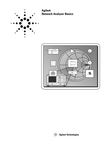
Transcription
White PaperVector Network Analyzer (VNA)Calibration: The BasicsBy Michael HiebelNote: VNA calibration has been the subject ofhundreds of papers, and when discussed in termsof its mathematical derivation can be quite complex.The goal of this white paper is far less academic, andincludes an overview of VNA calibration, a discussionof calibration standards and techniques, along withguidelines that can help designers choose the bestcalibration technique for specific situations. It alsoprovides tables showing the applicability of the various calibration techniques and the influence of variousactions that affect the calibration. A more thoroughtreatment of the subject can be found in the 420-pagebook by Rohde & Schwarz author Michael Hiebelentitled “Fundamentals of Vector Network Analysis,”which is available from the Book Shop on theRohde & Schwarz web site (www.rohde-schwarz.com).The most common measurement task in RF and microwave engineering involves the analysis of circuits using a network analyzer (VNA). This versatile instrumentcan evaluate nearly all types of devices, from filtersand amplifiers to complex multifunction subsystems.The reason the instrument is so widely used is thatit can, through the use of scattering (S)-parameters,evaluate the characteristics of the device under testwith a high level of precision. S-parameters have longbeen the chosen method for this because they arerelatively easy to derive at high frequencies and aredirectly related to the measurement parameters ofinterest to microwave designers, such as gain, returnloss, and reflection coefficient. They are also extremelywell suited for use by the electronic design automationtools that designers have come to rely on.A VNA is only as useful as the accuracy with whichit makes measurements, and this requires theinstrument to be calibrated. The calibration processemploys a technique called vector error correction,in which error terms are characterized using knownstandards so that errors can be removed from actualmeasurements. The process of removing these errorsrequires the errors and measured quantities to bemeasured vectorially (thus the need for a vector network analyzer). In contrast, scalar network analyzerscan only record the magnitude of the measured quantities, precluding them from being used to eliminatesystematic measurement errors, which unlike randomerrors, can be mathematically eliminated from themeasurement result.Perhaps the most simplistic analogy to the VNA calibration process is “zeroing out” test-lead resistancefrom an ohmmeter. This early form of “de-embedding” the test lead resistance from the measurementresults is far less complicated but no less relevant thancalibration performed on a VNA. Of course, A VNAis a vastly more complex instrument than a simpleohmmeter, as is its error model that includes multipleterms for every frequency at which measurementsare made.
The ideal VNA error model includes all possible areasin which systematic inaccuracies can arise, includingdirectivity of the couplers, the match presented by thereflectometer via its test port, the frequency responseof the reflectometers and transmission betweenports, and crosstalk between ports. A typical VNAerror model is shown in Figure 1. Calibration providesaccuracy whether the measurement plane resides atthe connector on the instrument’s front panel or theconnectors at the end of test cables.was of “commercial grade” and although not specifiedfor use for precision measurements is widely used inmicrowave systems of many kinds.The second set was a high-performance type designedfor VNA measurements. In the figures, phase and amplitude of the transmission coefficient are displayed.The results of the first measurement were saved,and both sets of cables were reformed to a specificbending radius and angle and measured again. Theresults show the significant improvement obtainedusing high-performance test cables – a factor of 10 inphase and 100 in amplitude (note the scaling!) whichare designed to maintain their performance within avery narrow range of variance within their specifiedbending radius. (For more information on the handlingof cables and connectors, see “A recipe for cable andconnector care,” page 9).Figure 1: Typical network analyzer error modelThe preceding simplistic description belies the widevariety of pitfalls that can singly or together degradeor invalidate the calibration process. Some are difficultto conceptualize and require considerable expertise,but others are as simple as making sure measurementsetups, such as cables and connectors, are handledwith care and that no stresses are placed on themthat exceed their specifications. Even the choice oftest cable can be extremely important, since cablesdesigned for the VNA environment are generally themost precise. For example, Figures 2a and b show theresults of a simple test. Two sets of cables 1 m longwere connected to a VNA and their ends connectedusing a through standard. The first set of test cablesMeasurement performance also depends on the accuracy and quality of the error model and calibrationstandards, and the repeatability of the measurementsystem itself. Even though created to reduce errors totheir lowest possible levels, a calibration performedpoorly can actually introduce errors that otherwisewould not have occurred. In short, a VNA can provideresults only as accurate as the information it isprovided. For example, the impedance employed inthe calibration must be precisely specified, as mustinformation about the calibration standard. Fortunately, the capabilities of modern VNAs as well asoptional automatic electronic calibration have madethe once-tedious, error-prone process of calibration farless difficult.Figure 2: Deviation caused by bending of two RG400 cables that are 1-m long (a), and forhigh-performance test port cables (b)
THE CALIBRATION PROCESSBefore going further, it is important to keep in mindthat every measurement is subject to measurementuncertainly, which is the statistical deviation of themeasured values from their true value. In the measurement domain, there are two types of uncertainties – random and systematic. Random errors varywith time and are thus unpredictable. While they canbe described, they cannot be removed by calibration. Typical random errors include those caused byinstrument noise, and the repeatability of switches,cables, and connectors. In contrast, systematic errorsoccur in a reproducible manner. They are caused byimperfections in the VNA, can be characterized, andthus can be removed mathematically through calibration. Another type of error called drift occurs after acalibration has been performed because of changes inVNA performance arising from variations in ambienttemperature. However, these errors can be removed byperforming additional calibrations.Since random errors cannot be removed throughcalibration, they must be reduced in severity asmuch as possible by following prudent measurementpractices, such as allowing the instrument to achievethermal equilibrium, using high-quality cables andconnectors, reducing system noise figure by keepingstep attenuator values as low as possible, selectinga small IF bandwidth, and possibly using averaging.Finally, as the interface between instrument, cable,DUT, test fixture, and in the case of semiconductorsthe wafer probe, the connector is a critical elementin achieving good measurement results. Connectorsmay look mundane, but they are fragile, precisionmachined components and are highly sensitive tocare in handling.process. An example of raw and corrected system datais shown in Table 1.System dataRaw system dataEffective system dataReflection tracking 2 dB 0.04 dBDirectivity 29 dB 46 dBSource match 22 dB 39 dBTransmission tracking 2 dB 0,06 dBIsolation 130 dB 130 dBLoad match 22 dB 44 dBTable 1: Comparison of typical raw and effective system dataThe calibration process determines the error terms,requires a test system consisting of a VNA, cables,and generally a test fixture, and is performed bysequentially making measurements using calibrationstandards. These calibration standards are one-portand two-port networks that have known characteristics. The chosen calibration process determines theproperties of the standards that must be used. It isimpossible to manufacture a calibration standard thathas ideal properties, so the deviations of the standards are sent to the VNA as characteristic data. Thisdata is provided as data files on digital storage mediaranging from a diskette to USB flash drive along withthe calibration standards and a printed measurementreport (Figure 3).ERROR TERMSEach network analyzer can be separated into an errornetwork (or linear error model) and an ideal networkanalyzer. The parameters of the error network areconsidered error terms (or correction data), and canbe directly interpreted as raw system data. Correctingsystem errors is the primary goal of calibration, andany remaining errors are expressed by the effectivesystem data and depend on the accuracy of the error terms and the repeatability of the measurementFigure 3: The Rohde & Schwarz R&S ZV-32 3.5-mm calibration kitand calibration data on disketteAfter calibration, the analyzer computes the error terms using the values it measured during thecalibration process along with the characteristic dataof the standards. It is then possible to correct the rawmeasured values in later measurements and calculate
S-parameters for the device under test. The interfacebetween the error network and the device under testis called the reference plane. When using coaxial calibration standards, the reference plane is the matingplane of the outer conductor, an example of which isshown in Figure 4.Reference planeFigure 4: Location of the reference planein a Type-N connectorthe need to transfer all the data using a separate storage medium.Coaxial calibration standardsShort (S)A coaxial short (Figure 5) can be constructed that hasnear ideal characteristics, with a total reflection ofmagnitude 1. The reflection coefficient of the short isdependent only on its length offset, which representsthe length between the reference plane and the short.The loss occurring over this length can generally be ignored. Modeling the short in a VNA requires that onlyits electrical length be entered into the instrument, butin some cases the model can be extended using thepolynomial coefficients L0 to L3 to account for parasiticinductance.CALIBRATION STANDARDSThe process of measuring the characteristic data iscalled characterization and must be performed inaccordance with principles established by various metrological organizations. In the U.S., this organizationis the National Institute of Standards and Technology(NIST, formerly the National Bureau of Standards). Thecharacterization should ideally be certified at regularintervals by an accredited measurement laboratoryto ensure that changes have not occurred that wouldaffect the accuracy of the results.The standards are described by using special coefficients because they provide a compact solution.Even over a frequency range of DC to 40 GHz, onlyseven coefficients are required per standard.The standards are also described using complexS-parameters that can be saved in one of the popularelectronic design automation (EDA) file formats, suchas Touchstone, which eliminates the need to extractthe coefficients manually, which can reduce accuracy.Since the S-parameter data files are generally quitelarge, they are provided on some form of digital media.VNA manufacturers also offer electronic (automatic)calibration, which has greatly simplified the calibrationprocess and eliminates the time-consuming, errorprone process of switching manually between variouscalibration standards. Characteristic data is stored inthe electronic calibration equipment, which eliminatesFigure 5: Short calibration standard.Open (O)A coaxial open standard (Figure 6) is constructedusing a closed design to avoid effects caused by entryof stray electromagnetic energy. At the open end ofthe inner conductor, a frequency-dependent fringingcapacitance is formed. Even if an open standard couldphysically be constructed with a length of 0, fringingcapacitances would result in a negative imaginary partfor S11 at higher frequencies.lC e(f)RarasiticfringingcapacitancesReference planeFigure 6: Open calibration standard.
Match (M)A match is a precision broadband impedance thathas a value corresponding to the system impedance.An implementation in which the inner conductorterminates into a resistively-coated substrate is shownin Figure 7. Using trimming holes created by a laser,it is possible to optimize the impedance value so thatreturn loss of 45 dB is achievable up to about 4 GHz.It was standard practice for many years to assume anideal match in the calibration process. However, VNAsnow include the non-ideal properties of a match aswell.Transition from coaxial tocoplanar modeResistive coating withtrimming holesReference planeFigure 7: Match standard, implemented asa terminating load.The characteristic impedance Zc of the air line is calculated from the diameter a of the inner conductor andthe inner diameter b of the outer conductoras follows:(Equation 1)Because the formula contains the ratio values a andb and not their absolute values, it is possible to matchthe mechanical properties of the air line to the type ofconnector being used. As a result, the transition fromthe connector to the air line is quite free of discontinuities. A cylindrical ferrite rod is introduced intothe air line that absorbs a considerable portion of theelectromagnetic energy at frequencies of 2 GHz andabove. At the input of the sliding match there is returnloss of about 20 dB, and if the rod is moved along theline, the length offset changes as does the phase ofthe reflection coefficient at the line input.Sliding Match (also called a sliding load or slidingtermination)A sliding match cannot be used at frequencies below2 GHz. However, almost all calibration techniquescan be performed using a sliding match and a fixedmatch to circumvent this low-end frequency-rangerestriction. At frequencies above about 8 GHz, a slidingmatch is considerably more accurate than a match.The TOM-X calibration technique cannot be performedusing a sliding match. An air line sliding match (Figure8) that has a specified characteristic impedance canbe manufactured much more accurately than thematch shown in Figure 7.Figure 9: Excerpt from the Smith chart fordetermining characteristic impedanceAt a constant frequency, the reflection coefficient ofthe sliding match lies at a different point on the circleof a Smith chart shown in green in Figure 9, depending on the length offset. Three points on the circleare sufficient to construct the center point Γm , whichcorresponds to the characteristic impedance of the airline section as measured by the VNA. For calibrationpurposes, this quantity is used instead of the impedance of the match in Figure 7. The circle radius isdetermined by the return loss of the ferrite rod.Figure 8: Sliding match
In practice, frequency sweeps are performed insteadof fixed-frequency measurements, so it is no longeracceptable to measure just three positions of the ferrite rod. If the frequency is increased, the three pointsmove along the circumference of the circle. However,frequency dependence of the points is not identical sothey move at different speeds, and at certain frequencies two or three points will overtake one another andmerge into a single point. In constructing the centerpoint, at least three separate points are required,distributed over the circumference of the circle. To ensure this occurs in the frequency range of the slidingmatch, six positions are selected on the match.Through (T)A through (Figure 11) is a two-port standard that allows direct connection of two test ports with low loss.The characteristic quantities of a through are insertionloss and electrical insertion length. In most commoncalibration techniques, the through is assumed to beideally matched. If connectors of the same type butof a different gender are used, the two test ports canIt is not necessary to approach a specific position onFigure 11: Through calibration standardFigure 10: Sliding match and pin depth gage keypoints notedthe Smith chart with exceptional accuracy. Instead,it is acceptable to orient the calibration proceduretoward the marks on the sliding match (points 1 to 6on Figure 10). Using the pin and fastening nut (points7 and 8), the offset of the inner conductor can beadjusted with respect to the reference plane for theconnector using a pin-depth gage. The “0” point onthe gage is generally aligned with a gage masterbefore using the device. If the inner conductor ofthe sliding match protrudes too far the connectorscan be damaged when connecting the match to thetest port. If the inner conductor is seated too low, anunnecessary air gap will be produced, which reducesaccuracy. It’s important to note that a pin depth gage,like all measurement instruments, has measurementuncertainty. Consequently, it is quite risky to adjust thepin depth to an exact “0” with the gage. In practice, aclearance of about 0.010 mm (depending on the connector system and the gage used) is desirable.be directly connected to produce a through connection. This special case of a through has an electricalinsertion length of 0 mm. If connectors of the sametype and gender are used, a through will consist of asmall line section, making a good electrical connectionbetween the two test ports. The characteristic impedance of the connection should match the referenceimpedance as closely as possible.Standards with Partially-Unknown Parameters forSeven-Term Calibration TechniquesReflect (R)This one-port standard, which like all of the standardswithin this section has only partially-known S-parameters, shows a reflection coefficient of magnitude 1. Theexact reflection is not required for the TRL calibrationtechnique but must be identical at both test ports. Thereflect standard is used for self-calibration techniquesin which the known information for the standardsis used to determine their unknown properties. Thephase of the reflect standard must be known to within /-90 deg. To characterize this type of standard, its behavior at lower frequencies is considered to be eithermore capacitive or more inductive. If the length offsetof the standard causes the phase to reside outside theinterval 0 deg to -90 deg. or 0 deg. to 90 deg., thelength offset must also be approximately known.
Line (L)Unknown Through (U)The line is a two-port standard and in coaxial systemsis implemented as an air line. The critical quantityof the line is its characteristic impedance, which ismatched as precisely as possible to the referenceimpedance using a proven mechanical design as inEquation 1. The electrical length of the line must bedifferent than the length of the through being used.The difference in length between the through and theline must not be equal to an integral multiple of halfthe wavelength because the calibration techniqueswould produce a singularity. The frequency range forcalibration using the line standard is restricted by thefact that the phase difference between transmissioncoefficients of the through and line must be sufficiently different form 0 deg. and 180 deg. That is, itmust be between 20 deg. and 160 deg. or the ratio ofthe stop and start frequencies may have a maximumratio of 8:1.Any two-port network whose S-parameters fulfill thereciprocity conditions S21 S12 can be used as an unknown through when the UOSM calibration techniqueis used. The phase shift of the unknown through mustbe known to some degree. If a two-port device undertest fulfills the reciprocity requirement, it too can beused as an unknown through. However, an isolatingnetwork or S21 S12 0 cannot serve as an unknownthrough.To extend this frequency range, two lin
Aug 08, 2019 · entitled “Fundamentals of Vector Network Analysis,” which is available from the Book Shop on the Rohde & Schwarz web site (www.rohde-schwarz.com). _ The most common measurement task in RF and micro-wave engineering involves the analysis of circuits us-ing a n