Transcription
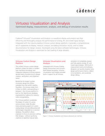
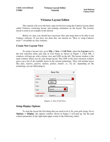
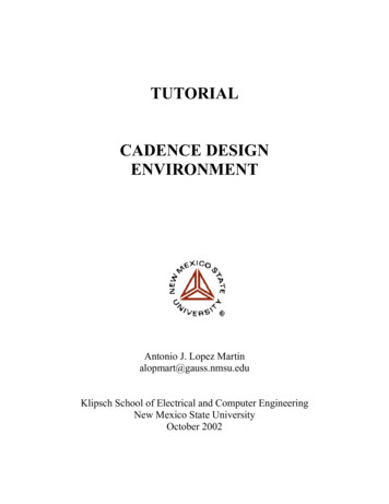
Virtuoso System Design PlatformUnified “system-aware” platform for IC and package designThe Cadence Virtuoso System Design Platform is a holistic, system-based solution that provides thefunctionality to drive simulation and LVS-clean layout of ICs and packages from a single schematic.There are two key flows: implementation and analysis.The implementation flow is used to create an IC package schematic in Virtuoso Schematic Editor andthen transfer the schematic data to Cadence SiP Layout to layout the physical design. In addition, thisflow offers the capability to generate and verify library parts, output a bill of materials (BOM), andperform layout versus schematic (LVS) checking.The analysis flow is used to extract and simulate any portion of the system (IC-package-PCB) regardlessof the layout design status. Moreover, this flow offers the capability to automatically generateschematics for the PCB and IC package layouts, bind the instances of the IC package to the ICschematic or models, and build testbenches to simulate the system using the Virtuoso ADE ProductSuite plus Spectre Multi-Mode Simulation interface. Cadence Sigrity models extracted from the PCBand IC package layouts get automatically stitched into the generated schematic.Seamless package/board-level layout parasitic back-annotation flowVirtuoso “Chip” ViewVirtuoso SchematicRepresenting System-Level DesignCadence SiP LayoutSingle source schematic automates package-level LVSAutomated package-level library developmentAllegroLibGaNConstraintsConnectivityIC to package co-design flow with LVL checkingAllegro FootprintsSi LVSGaAsSip DesignSiGaAsGaNVirtuoso SE SymbolVirtuoso SE SymbolVirtuoso SE Symbol26SN750.01 µf143786500 KΩVolume470 pHQ1T1R2ROutside Sourced DesignVirtuoso DesignVirtuoso DesignFigure 1: Virtuoso System Design Platform FlowSigrity ExtractedInterconnect ModelHPJRSTKEYVIDAUDSPVSSRX1TX1RGBVCC
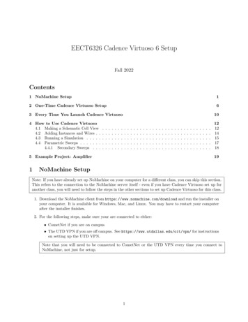
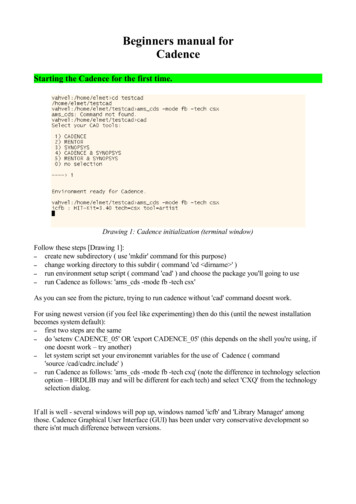
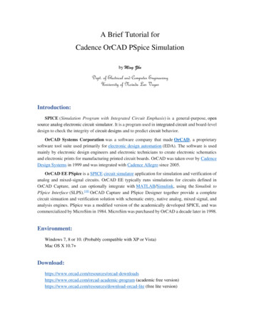
Virtuoso System Design PlatformIntroductionThe task of designing a chip that meetsall product expectations once placed intoa package and then onto a PCB is verychallenging. With the recent growth inheterogeneous integration, now considerdesigning multiple chips, across multipletechnologies, that integrate onto a singlepackage and then are integrated ontoa PCB. For even the most experienceddesigners, this can be a frighteningproposition.identify and eliminate such errors atan early design stage and long beforetapeout, it is essential to have a familiardesign and simulation environment thatauto-enables the IC designer to simulatethe IC in context of the entire PCB andpackage system and its parasitics. Whilesuch an environment exists for simulatingI/O to I/O interconnects for digital ICs,the Virtuoso System Design Platform isthe first seamless flow of its kind thatallows simulation of the analog/RF IC incontext of a complete PCB/package circuitUnification of the Virtuoso and Allegro/Sigrity PlatformsICPackagePCBFigure 2: How IC, package, and PCB relateToday, designing at the “systemlevel” (IC-package-PCB) involves a lotof educated guesswork regarding thedownstream effects of the package/PCBon the performance and reliability ofyour chip(s). The Virtuoso System DesignPlatform takes this guesswork out ofdesigning chips accounting for systemlevel effects.Traditionally, the analog/RF IC designerwould only simulate standalone ICswithout considering the effects of thepackage and PCB. The package containsa single or multiple ICs and interconnects.It also probably contains discrete components required by the ICs to function.Similarly, the PCB contains severalpackages and interconnects and discretecomponents. It is important to simulatethe entire system together to capture theperformance at high frequencies. Becausethe IC designer and the package designeruse different schematic entry tools, theIC designer must re-capture the packagesystem schematic as a testbench aroundthe IC schematic to do combined systemsimulations. Earlier, such system analysishad been largely a manual effort witherror-prone stitching of package modelsto the rest of the system schematic. Towww.cadence.cominclusive of parasitics. This flow empowersthe IC designer and minimizes designiterations.The Virtuoso System Design Platformprovides an IC-centric solution withboth a top-down implementation flowand bottom-up analysis-centric flow.The analysis-based flow helps bring inthe complete simulation environment,requiring minimal knowledge in PCB orpackage and electromagnetic simulationdomains. A colossal improvement inproductivity is predicted with such anintegrated solution.The Virtuoso System Design Platformimplementation flow provides thecapability to drive IC and packagelayout through a single schematiceditor. By having the same schematiceditor (Virtuoso Schematic Editor), theIC designer is in a much better positionto do system-level design in a commonenvironment with pre-layout systemsimulations (IC and package together) andthen drive the layout of the respectivedomain. This flow also automates muchof the package-level library developmentprocess by generating die footprints to beused in SiP Layout. Advanced users caneasily co-design between the die and thepackage to achieve better package-levelrouting and/or wire bonding.The Virtuoso System Design Platformanalysis flow allows the IC designer toimport a PCB and package layout withits corresponding parasitic models, represented by S-parameters or SPICE, to theIC design environment. The flow reads thePCB or package connectivity and creates aschematic with parasitic models stitchedin. The schematic becomes ready tosimulate in context of the PCB or packagesystem.The Virtuoso System Design Platformenvironment helps to integrate andsimulate the IC in context of all suchpackage/PCB interconnects and externalcomponents. This assumes greater importance because the IC, package, andPCB are typically designed by differentteams using different design tools acrossgeographic locations, all independentof the others and at different stages ofthe design cycle. The Virtuoso SystemDesign Platform brings the package andPCB-level layout parasitics into a commonschematic, enabling cross-domainsimulation of the complete system. Thishelps designers identify critical performance deviations before tapeout.Communication of required modificationscan then be driven directly to package/PCB teams.An important feature here is to intelligently stitch the parasitics models intothe simulation schematic. If the modelsalso contain discrete devices, they shouldbe auto-filtered when the simulationschematic is created so that they are notdouble-counted in the simulation.2
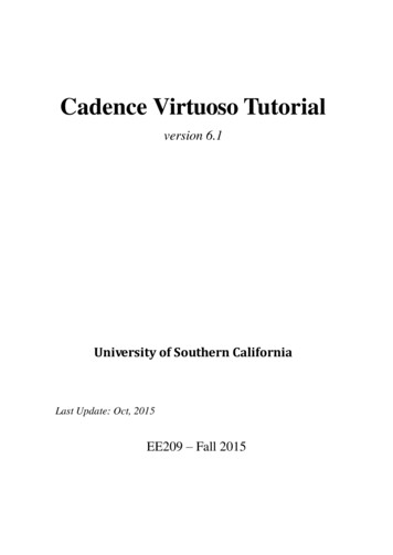
Virtuoso System Design PlatformVirtuoso System DesignPlatformThe Virtuoso System Design Platform flowtraces through the following productsin the IC, package, PCB, and EM solverdomains: Virtuoso Schematic Editor: For creatingthe package schematic Virtuoso Layout Suite: For die export Cadence SiP Layout XL: For design andlayout of multi-die packages Sigrity EM solvers: For extractingmodels of PCB and package Spectre Multi-Mode Simulation: Forenabling system simulationsThere are primarily two flows in theVirtuoso System Design Platform, theimplementation and the analysis flow.The implementation flow allows you todesign schematics of packages in theVirtuoso Schematic Editor before pushingit to a package layout editor. It furtherallows you to export die footprints andsymbols from the Virtuoso Layout Suiteand use them to construct a packageschematic. The bidirectional flow ofdata dynamically propagates edits in theschematic to SiP Layout and conversely.Generating a BOM, visualizing designdifferences in an intuitive manner, andlooking at layout reports constitute someof the other key features of this flow.Once your package or PCB is designedusing the implementation flow describedabove, the analysis flow lets you importPCB and package layout in the Virtuosoenvironment as a schematic along withthe automatically stitched parasitic modelsof the components and traces early in thedesign cycle, and carry out a parasiticaware system-level simulation. You cansimulate such a system, identify criticalperformance metric deviation early, andcommunicate required modifications tothe package and PCB teams.Virtuoso System Design PlatformVirtuosoArbitrary Structure ModelingParasitic ExtractionDFIILibraryDevice Model Mapping FilePackage/PCBDomainSigrityConnectivity/Discrete Devices and LVSAllegroLibrarySmart N-Port S-ParametersBOMBidirectional Connectivity/Constraints with LVSDFIILibraryVirtuoso ADE-MTS Circuit SimulationIC DomainIC Layout and Package/Module-Level SchematicPhysical Package and PCB DesignAllegroImplementation (Top-Down) FlowAnalysis (Bottom-Up) FlowFigure 3: The Virtuoso System Design Platform flowBenefitsBy integrating the Virtuoso, Allegro,Sigrity, and Spectre platforms, theVirtuoso System Design Platform entailsthe following three key benefits: Updates the IC layout and packagelayout design using the VirtuosoSchematic Editor. Therefore, in additionto the IC layout, you can now designthe schematic for a package layout. TheVirtuoso Schematic Editor provides asingle schematic editor-driven IC andpackage design.www.cadence.com Creates a package or PCB parasiticaware schematic that can be simulatedwith the Virtuoso Analog DesignEnvironment including multi-technologysimulations. This is an essentialmechanism to realize complete systemaware simulations. Designs IC and package layout throughthe co-design die abstract flowsimultaneously. This minimizes designiterations and cuts down on very-latestage floorplanning and designfeasibility issues.FeaturesDie exportThe Virtuoso System Design Platformprovides a key feature to generatefootprint and symbol information from aVirtuoso layout for use in constructing apackage schematic and a package layout.This also allows simultaneous co-designof the IC and package layout and helpsminimize design iterations.3
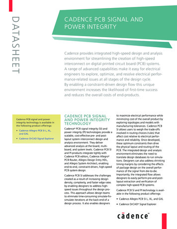
Virtuoso System Design PlatformSchematic SymbolPreserved Logical IntentIC LayoutDie AbstractFigure 4: Die abstractsCreating a project and assigningpart table filesWhile creating a package schematic, it isimperative to efficiently select parts thatare supplied by a vendor. The part tablefile option lets you seamlessly select fromas many as a million parts from differentvendors and assign them effectively onthe instances in your schematic.Transferring the schematicinformation to SiP LayoutOnce the schematic with all the parts iscreated, this feature enables the seamlesstransfer of the schematic information tothe SiP Layout editor. Subsequently, youcan place all the parts in the SiP Layouteditor and start creating routes andcomplete the finished package.Editing in the SiP Layout andback-annotating in the VirtuosoSchematic Editorences in a highly intuitive and graphicalmanner utilizing the Annotation Browserassistant in the Virtuoso Schematic Editor.During a design cycle, it is quite possiblethat the layout engineer recommendschanges that need to be matched inthe Virtuoso Schematic Editor. Thisfeature enables transferring informationseamlessly to the Virtuoso SchematicEditor and ensures that the schematic andlayout are always in sync.Generating a BOM reportDesign-differentiating layout vs.schematic checkA BOM report lists all the componentsused in a design along with the partnumbers and values of the differentproperties of each component. This is anextremely important input for an originalequipment manufacturer (OEM). TheVirtuoso System Design Platform providesa user-friendly and highly customizableenvironment to generate all such reports.Provides a signoff-quality LVS checkhighlighting nets, components, andsimilar differences between the layout andthe schematic. It also flags design shorts,unplaced components on the layout,and DRC checks. It reports all the differ-Figure 5: Selecting a package-level part from the part table file in the implementation schematicwww.cadence.com4
Virtuoso System Design PlatformFigure 6: Schematic driving package layoutAnalysis Flow FeaturesYou can start utilizing the analysis flowonce you have the design of a fully routedpackage.Creating a parasitic-aware PCB/package schematic in VirtuosoSchematic EditorAnother key feature enables you tocreate a PCB or package schematic withS-parameters and SPICE models of thetraces and PCB or package componentsautomatically stitched in, all using theVirtuoso Schematic Editor.It is noteworthy to highlight the analysisflow ability to use a device mapping textfile to automatically replace SMDs withtheir corresponding vendor-specifiedS-parameters and SPICE models whilecreating the schematic. Previously, theschematic creation with all the models inplace was a manual, tedious, and errorprone process.Binding the IC footprint to itsunderlying schematic or sub-circuitmodelAutomatic creation of testbenchsymbol for top-level systemsimulationsOnce the parasitic-aware schematic iscreated, the IC is imported as a simplefootprint. The next important step isto bind this footprint to the original ICschematic symbol or sub-circuit. This isthe same symbol that the IC designerhas been using in the top-level IC simulations. The Virtuoso System DesignPlatform provides an intelligent mappingmechanism to create a 1:1 map betweenthe footprint terminals and the IC symbolterminals. In cases where a schematic or aschematic symbol is not present, it allowsbinding to a sub-circuit model of the IC.Creation of a testbench symbol is aneasy, automatic, and seamless feature oftestbench generation and is an integralpart of the analysis flow. It reduces thedesign time and creates compact andmanageable testbenches for you to startan early evaluation and subsequent fix ofthe system.Simulation layout vs. schematiccheckThe simulation layout versus schematiccheck feature helps to flag any differences between the created schematic andthe layout from which it was originallycreated. This feature is essential becausevery often a designer tends to tweakhis top-level schematic to arrive at thedesired results.Figure 7: Viewing LVS differences highlighted in the Annotation Browserwww.cadence.com5
Virtuoso System Design PlatformSpecificationsPlatform/OSCadence Services and SupportThird-party support Linux for tools based on Virtuosoplatform Linux, Microsoft Windows fortools based on Allegro and Sigritytechnologies Cadence application engineers cananswer your technical questions bytelephone, email, or Internet—they canalso provide technical assistance andcustom training Design libraries including parasiticmodels (SPICE and S-parameters)Tools that may be required to runthe Virtuoso System Design Platformflow Virtuoso Layout Suite die Cadence-certified instructors teachmore than 70 courses and bringtheir real-world experience into theclassroom Virtuoso Schematic Editor XL Allegro PCB/package layout Virtuoso Layout Editor Sigrity models representing parasiticmodels of the traces and componentson the PCB/package Virtuoso Analog Design EnvironmentAllows seamless import of third-partyvendor-supplied models of SMDs into theparasitic-aware PCB/package schematicDesign input Device models of SMD’s SiP layout Virtuoso Schematic Editor schematic Parasitic-aware simulation schematic Footprint of dies designed in VirtuosoLayout Suite Spectre Multi-Mode Simulation,Spectre RF Option Allegro SiP and PCB layout editor Sigrity PowerSI , Sigrity PowerSI 3DEM Extraction Option, and SigrityXtractIM technology More than 25 Internet LearningSeries (iLS) online courses allow youthe flexibility of training at your owncomputer via the Internet Cadence Online Support gives you24x7 online access to a knowledgebaseof the latest solutions, technicaldocumentation, software downloads,and more For more information, please visitwww.cadence.com/support for supportand www.cadence.com/training fortrainingCadence software, hardware, and semiconductor IP enable electronic systems and semiconductor companiesto create the innovative end products that are transforming the way people live, work, and play. Thecompany’s Intelligent System Design strategy helps customers develop differentiated products—fromchips to boards to intelligent systems. www.cadence.com 2019 Cadence Design Systems, Inc. All rights reserved worldwide. Cadence, the Cadence logo, and the other Cadence marks found atwww.cadence.com/go/trademarks are trademarks or registered trademarks of Cadence Design Systems, Inc. All other trademarks are theproperty of their respective owners. 9618 08/19 SA/SS/PDF
The Virtuoso System Design Platform brings the package and PCB-level layout parasitics into a common schematic, enabling cross-domain simulation of the complete system. This helps designers identify critical perfor- mance deviations before tapeout. Communication of required modifications can then be driven directly to package/ PCB teams.