Transcription
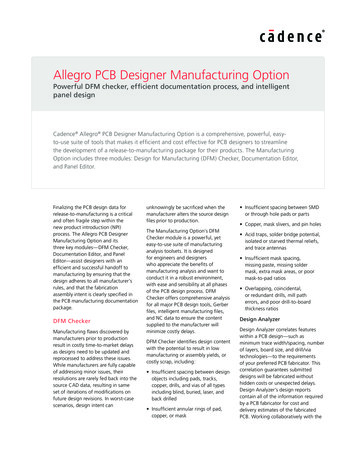
Allegro PCB Designer Manufacturing OptionPowerful DFM checker, efficient documentation process, and intelligentpanel designCadence Allegro PCB Designer Manufacturing Option is a comprehensive, powerful, easyto-use suite of tools that makes it efficient and cost effective for PCB designers to streamlinethe development of a release-to-manufacturing package for their products. The ManufacturingOption includes three modules: Design for Manufacturing (DFM) Checker, Documentation Editor,and Panel Editor.Finalizing the PCB design data forrelease-to-manufacturing is a criticaland often fragile step within thenew product introduction (NPI)process. The Allegro PCB DesignerManufacturing Option and itsthree key modules—DFM Checker,Documentation Editor, and PanelEditor—assist designers with anefficient and successful handoff tomanufacturing by ensuring that thedesign adheres to all manufacturer’srules, and that the fabricationassembly intent is clearly specified inthe PCB manufacturing documentationpackage.DFM CheckerManufacturing flaws discovered bymanufacturers prior to productionresult in costly time-to-market delaysas designs need to be updated andreprocessed to address these issues.While manufacturers are fully capableof addressing minor issues, theirresolutions are rarely fed back into thesource CAD data, resulting in sameset of iterations of modifications onfuture design revisions. In worst-casescenarios, design intent canunknowingly be sacrificed when themanufacturer alters the source designfiles prior to production.The Manufacturing Option’s DFMChecker module is a powerful, yeteasy-to-use suite of manufacturinganalysis toolsets. It is designedfor engineers and designerswho appreciate the benefits ofmanufacturing analysis and want toconduct it in a robust environment,with ease and sensibility at all phasesof the PCB design process. DFMChecker offers comprehensive analysisfor all major PCB design tools, Gerberfiles, intelligent manufacturing files,and NC data to ensure the contentsupplied to the manufacturer willminimize costly delays.DFM Checker identifies design contentwith the potential to result in lowmanufacturing or assembly yields, orcostly scrap, including: Insufficient spacing between designobjects including pads, tracks,copper, drills, and vias of all typesincluding blind, buried, laser, andback drilled Insufficient annular rings of pad,copper, or mask Insufficient spacing between SMDor through hole pads or parts Copper, mask slivers, and pin holes Acid traps, solder bridge potential,isolated or starved thermal reliefs,and trace antennas Insufficient mask spacing,missing paste, missing soldermask, extra mask areas, or poormask-to-pad ratios Overlapping, coincidental,or redundant drills, mill patherrors, and poor drill-to-boardthickness ratiosDesign AnalyzerDesign Analyzer correlates featureswithin a PCB design—such asminimum trace width/spacing, numberof layers, board size, and drill/viatechnologies—to the requirementsof your preferred PCB fabricator. Thiscorrelation guarantees submitteddesigns will be fabricated withouthidden costs or unexpected delays.Design Analyzer’s design reportscontain all of the information requiredby a PCB fabricator for cost anddelivery estimates of the fabricatedPCB. Working collaboratively with the
Allegro PCB Designer Manufacturing OptionSilkscreen-related analysis includes inkover pads, ink over mask exposures, andother checks. Less-than-minimal partspacing, pad spacing between adjacentparts, and minimal spacing betweencomponent pads and adjacent vias, drills,and copper objects are examples ofcomponent-related analysis.Figure 1. Use of hierarchical rule sets helps identify defects, avoiding costly bareboard scrapreport in hand, PCB fabricators can makerecommendations for design changesthat result in significant cost and timesavings while maintaining design intent.Design Analyzer bridges the gap betweenengineer and PCB fabricator by extractingkey information about the PCB andpresenting it in an easy-to-read format.Hierarchical Rule-Set-Driven AnalysisManage the myriad of checks and theanalysis process by creating rules sets.Checks are organized into layer types andsub-categories to simplify the selectionof checks to perform and the setting ofcorresponding parameters. Define thetype and order of a group of checks (ruleset) to be performed. Analysis can includenetlist or layer comparison, design ruleverification, fabrication, and assemblychecks on the entire design, a specificlayer, or a region of the design. Thisdramatically reduces set up and executionof the analysis. Analysis rule sets can besaved and recalled for use on any design.Rule sets can be defined for a specific PCBtechnology, vendor capability, or uniquedesign requirement.For many designs, different regions orlayers of a PCB have unique constraintsand subsequently require custom analysis.Use unique rule hierarchy to tailor ananalysis to bare board construction, boarddensity, or component technology.www.cadence.comPCB Fabrication AnalysisFabrication analysis will detect specificdesign content that might have anadverse effect on PCB fabrication.Features such as less-than-minimalspacing, acid traps, minimal annular rings,minimum features sizes, and copper andmask slivers are just a few examples ofthe fabrication analysis available. Drillrelated analysis includes minimal distancesbetween drills, pads without drills, millpath errors, coincident or overlappingdrills, and others.Figure 3. Silkscreen-to-solder-mask spacingviolationError ChartingLarge-scale analysis can often resultin a large number of reported failures.Viewing the results of large-scale analysisin chart form allows you to get to theroot of the failure and quickly ascertaina remedy. Charting allows you to reviewspecifics of the failures to identify trendsor unexpected results. DFM Checker’scharting feature reports the exact natureof the error and the PCB features relatedto that error. The charting functiongroups common errors so they can bequickly identified and resolved.Crossprobing with AllegroPCB EditorFigure 2. Acid trap violationPCB Assembly AnalysisAssembly analysis will detect specificPCB content that might have an adverseeffect on PCB assembly. Solder andpaste mask features—such as less-thanminimal mask spacing, missing masks,extra mask, minimal mask annular rings,and mask-size-to-pad-size ratios—areexamples of mask analysis available.The Manufacturing Option’s DFM Checkermodule is tightly integrated with AllegroPCB Editor to walk through errors. Selecterrors within DFM Checker and it zoomsinto the error location within AllegroPCB Editor. This expedites the process offinding and correcting errors in the sourcePCB design. DFM Checker adds DRCmarkers in Allegro Constraint Managerwith details of the violation.2
Allegro PCB Designer Manufacturing Optionnecessary to not only build the producttoday, but also any repeat builds in thefuture—eliminating any guesswork.The Manufacturing Option’sDocumentation Editor module is aPCB documentation-authoring toolthat intelligently automates yourdocumentation creation process toproduce complex PCB documentation ina fraction of the time versus traditionalmethods. Documentation Editor enablesyou to quickly create the manufacturingdrawings that drive PCB fabricationand assembly.Figure 4: Crossprobing between errors andAllegro PCB EditorAllegro PCB EditorAllegro Constraint ManagerFigure 5. Missing solder maskDocumentation EditorUtilizing the Allegro PCB CAD data,Documentation Editor creates intelligentlinked PCB views, drawing details,document notes, drill charts, parts lists,and other crucial documentation details.The result is documentation that moreaccurately articulates instructions forthe successful fabrication, assembly,and inspection of PCBs. The completeddocumentation release package containsall the data necessary to build, view, andarchive the final product.Documentation Editor includes thefollowing key features: Creation and placement of unlimitedviews of the PCB. Each view canhave its own display settings and canbe formatted independently of thesource data. Tight integration with Allegro PCBEditor enables simple click-throughpassing of design data to expedite thedrawing creation process Intelligent automation saves hours, ifnot days, creating PCB drawings forfabrication, assembly, and inspection Automatic creation of componentassembly views, drill pattern view,details, and parts lists derived fromthe Allegro PCB CAD data, eliminatesmanual drawing of tedious documentelements Design changes made in Allegro PCBEditor are automatically propagatedto all effected drawing elements,dramatically reducing time spentupdating documentation due to thedesign changesDrawing CreationStandard or custom drawing elements areeasily added by dragging and droppingfrom a palette of drawing-specificelements, such as sheet borders, titleblocks, PCB views, drill charts, detailviews, text boxes, and note blocks.Elements added to your drawings can beeasily relocated, resized, and customized.Each element can be scaled, formatted,and transformed (rotated, mirrored,flipped, etc.) independent of eachPCB documentation creates themanufacturing specification for anelectronic product. Comprehensivedocumentation records the engineering“intent” of a design specifying theform, fit, and function of the PCB.Documentation drives the procurementprocess, aids manufacturing engineering,and is used in final inspection toverify that the product was built toengineering’s specification. It also getsarchived to ensure later production runscan be repeated with the same level ofconsistent quality. PCB documentationmust capture all of the informationFigure 6. Produce complex PCB documentation in a fraction of the timewww.cadence.com3
Allegro PCB Designer Manufacturing OptionECO Updates MinimizeDocumentation ReworkAll drawing elements in DocumentationEditor are derived from the source AllegroPCB CAD data. Opening the reviseddesign in Documentation Editor allowsyou to perform lightning-fast engineeringchange order (ECO) updates by simplyrefreshing the source computer-aideddesign (CAD) data. When refreshed, alldrawing elements, such as PCB views,tables, details, parts lists, drill charts, etc.are updated with the new design data.All user customization for each elementis maintained during the refresh, furtherminimizing documentation rework.Figure 7. Drawing-detail wizards automate the layer stack-up, finger chamfer, andV-score drawingother. There is no limit on the numberof elements that can be placed ona drawing.Fabrication and Assembly DrawingToolsThe drawing tools include support foradding PCB views to fabrication andassembly drawings. You can drag anddrop views of the board outline, top/bottom side of the PCB, drill pattern,drill chart, integral parts list, componentcoordinate charts, and many others.Drawing detail templates automate thecreation of detail views of via stackups, layer stack-ups, finger chamfers,V-score, and several other commondrawing element types. Componentassembly PCB views can be filtered byvariant, or can apply variant status inparts lists. You can also create assemblyprocess documentation for processdriven PCB assembly, and easily createcolor-coded drawings for each assemblyprocess, process step charts, and processbased parts lists. Advanced capabilitiesalso include drawing functionality forgeometric dimensioning and tolerance(GD&T), coordinate dimensioning, blind/buried via support in via stack ups, PCBviews, and drill charts.Mechanical Component SupportDocumentation Editor understands thatPCBs are comprised of both electricaland mechanical components. Users canwww.cadence.comdefine any drawing item as a mechanicalcomponent and store it in a “gallery” forre-use. Mechanical components can alsobe associated to electrical components tohelp automate correct parts list quantitycalculations, particularly when assemblyvariants are also used. DocumentationEditor can construct a mechanicalcomponent in a number of differentways: Manually using DocumentationEditor’s drafting tools, by importing DXFobjects from a mechanical system, or byimporting any digital image file (JPEG,BMP, etc.) that the user wishes to depictas a mechanical component.Design-Driven DocumentationDocumentation Editor drawing contentis derived directly from the Allegro PCBCAD data. Components, pins, assemblymounting sides, layers, vias, nets,assembly variants, part attributes, drillholes and symbols, and other criticaldesign data are imported to ensuredocument accuracy. External contentsuch as JPEGs, BMPs, GIFs, and TIFFscan be imported and incorporated in thedrawings. OLE objects, audio, and videofiles can also be imported and linkedwithin the documentation and storedwith the documentation release package.In addition, Gerber and DXF files can beimported and exported.Pack and ReleaseUsers can select drawings and files andcompress them with an integrated viewerfor use with users who do not have aviewer or do not wish to install one.Template Customization ToolkitThe Template Customization Toolkitallows custom template creation andenables template tool pallet and formattemplate dialogs.Automation ToolkitThe Automation Tool Kit enables VBscripting tools to automate the processof creating PCB documentation. Youcan reduce the process of creatingdocumentation to a few clicks for a PCB.Panel EditorElectronics manufacturers often panelizesingle-board designs into arrays orsub-panels to facilitate their PCBassembly process. PCB CAD tools arevery good at designing the single-boarddesign or “one-up” PCB, but lack thenecessary functionality to design thevaried complexities and details that arerequired for panels. Documenting thefinished panel and adding features suchas pinning holes, fiducials, score lines, andbreakaway tabs can be difficult and timeconsuming in today’s CAD and computeraided manufacturing (CAM) tools.The Manufacturing Option’s Panel Editormodule intelligently automates thecomplex process of panel definition anddocumentation, simplifying the design4
Allegro PCB Designer Manufacturing OptionFigure 8. Automatically create panel arrays of PCBs on a panel documentation drawingprocess. This solution enables designersto quickly create electronic manufacturingdocuments that clearly articulate thepanel specification and instructions forsuccessful fabrication, assembly, andinspection of their designs.Panel Editor includes the following keyfeatures: Automatic array creation in spreadsheetor auto-calculate mode using imported,intelligent Allegro PCB design dataresults in an optimized panel thatincludes as many PCBs as possible Allows quick placement of top, bottom,drill pattern, or custom panel arrays ona drawing, as well as drill charts, noteblocks, mill, and V-score details Automatic NC milling definition allowsthe route path around a PCB to bedefined within a panel as well as thebreakaway tabs, then the NC millingcan be automatically applied to allthe PCBs within the panel as well asmerged route information for oneunified NC milling path Panel Drawing Detail wizards usethe existing PCB and NC milling datato automatically depict mill tab andV-score details Web Publisher allows for the creationof PCB release packages in HTMLformat Flip panel supportEase of Drawing CreationPCB designers often turn to CAM toolsfor their PCB assembly panel design,tools created specifically for the CAMengineer at the PCB fabricator that mostPCB designers find difficult to use. TheManufacturing Option’s Panel Editormodule is designed for ease of use, withdrag-and-drop drawing elements—including PCB views, charts, details, textboxes, and note blocks—that are treatedas drawing elements and can be quicklyadded and modified. Each element canbe independently scaled, formatted, andtransformed (e.g., rotated, mirrored,flipped). There is no limit on the numberof elements that can be placed on adrawing. Panel-level drill and coordinate chartsallow the user to place a drill andcoordinate charts reflective of all thePCBs contained in a panel to defineall components, hole sizes, locations,symbols, and quantities for the entirepanel. All of the formatting capabilitiesof the single-instance PCB drill andcoordinate chart are also supported forpanels. In addition, any pinning holesadded to the panel are automaticallyincluded in the drill chart. Coordinatecharts or the panel can be exportedin CSV format to drive pick-and-placemachinery.Figure 9. Panel Drawing Detail wizards use the existing PCB and NC milling data toautomatically depict mill tab and V-score detailswww.cadence.com5
Allegro PCB Designer Manufacturing OptionData ImportationCadence Services and SupportThe Manufacturing Option’s Panel Editormodule uses the Allegro PCB CAD datain the IPC-2581 format to drive the paneldefinition and documentation creationprocess. External content such as JPEGs,BMPs, GIFs, and TIFFs can be importedand incorporated in the drawings. OLEobjects, audio, and video files can alsobe imported and linked within thedocumentation drawings and stored withthe documentation release package. Inaddition, RS274X files can be importedand DXF can be imported and exported. Cadence application engineers cananswer your technical questions bytelephone, email, or Internet—they canalso provide technical assistance andcustom trainingAlways Up-to-Date ECOsThe panel definition and all drawingelements are derived from the sourceAllegro PCB CAD data and always remainlinked to that source data. These linksallow you to perform lightning-fast ECOsby simply refreshing only the source CADdata. When refreshed, all instances ofthe original Allegro PCB CAD data (arrayinstances, PCB views, tables, details, drillcharts, etc.) are refreshed to display thenew design data changes. All unique usersettings defined for each instance aremaintained during the refresh, furtherminimizing ECO documentation rework. Cadence certified instructors teachmore than 70 courses and bringtheir real-world experience into theclassroom More than 25 Internet LearningSeries (iLS) online courses allow youthe flexibility of training at your owncomputer via the Internet Cadence Online Support gives you24x7 online access to a knowledgebaseof the latest solutions, technicaldocumentation, software downloads,and moreCadence Design Systems enables global electronic design innovation and plays an essential role in thecreation of today’s electronics. Customers use Cadence software, hardware, IP, and expertise to designand verify today’s mobile, cloud, and connectivity applications. www.cadence.com 2015 Cadence Design Systems, Inc. All rights reserved worldwide. Cadence, the Cadence logo, and Allegro are registered trademarks of CadenceDesign Systems, Inc. in the United States and other countries. All other trademarks are properties of their respective holders.4455 04/15 SA/DM/PDF
by a PCB fabricator for cost and delivery estimates of the fabricated PCB. Working collaboratively with the Cadence Allegro PCB Designer Manufacturing Option is a comprehensive, powerful, easy-to-use suite of tools that makes it efficient and cost effective for PCB designers to streamline