Transcription
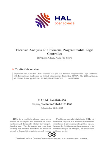
PGA280PGA280www.ti.com. SBOS487A – JUNE 2009 – REVISED SEPTEMBER 2009Zerø-Drift, High-Voltage,Programmable Gain INSTRUMENTATION AMPLIFIERCheck for Samples: PGA280FEATURESDESCRIPTION The PGA280 is a high-precision instrumentationamplifier with digitally-controllable gain and signalintegrity test capability. This device offers low offsetvoltage, near-zero offset and gain drift, excellentlinearity, and nearly no 1/f noise with superiorcommon-mode and supply rejection to supporthigh-resolution precision measurement. The 36Vsupply capability and wide, high-impedance inputrange comply with requirements for universal signalmeasurement.123 WIDE INPUT RANGE: 15.5V at 18V SUPPLYBINARY GAIN STEPS: 128V/V to 1/8V/VADDITIONAL SCALING FACTOR: 1V/V and1⅜V/VLOW OFFSET VOLTAGE: 3μV at G 128NEAR-ZERO LONG-TERM DRIFT OF OFFSETVOLTAGENEAR-ZERO GAIN DRIFT: 0.5ppm/ CEXCELLENT LINEARITY: 1.5ppmEXCELLENT CMRR: 140dBHIGH INPUT IMPEDANCEVERY LOW 1/f NOISEDIFFERENTIAL SIGNAL OUTPUTOVERLOAD DETECTIONINPUT CONFIGURATION SWITCH MATRIXWIRE BREAK TEST CURRENTEXPANDABLE SPI WITH CHECKSUMGENERAL-PURPOSE I/O PORTTSSOP-24 PACKAGESpecial circuitry prevents inrush currents frommultiplexer (MUX) switching. In addition, the inputswitch matrix enables easy reconfiguration andsystem-level diagnostics—overload conditions areindicated.The configurable general-purpose input/output(GPIO) offers several control and communicationfeatures. The SPI can be expanded to communicatewith more devices, supporting isolation with only fourISO couplers. The PGA280 is available in aTSSOP-24 package and is specified from –40 C to 105 C.RELATED PRODUCTSAPPLICATIONS HIGH-PRECISION SIGNAL INSTRUMENTATIONMULTIPLEXED DATA ACQUISITIONHIGH-VOLTAGE ANALOG INPUT AMPLIFIERUNIVERSAL INDUSTRIAL ANALOG INPUT 15VFEATURESPRODUCT23-bit resolution, ΔΣ analog-to-digital converterADS1259Chopper-stabilized instrumentation amplifier,RR I/O, 5V single-supplyINA333High-precision PGA, G 1, 10, 100, 1000PGA204High-precision PGA, JFET Input, G 1, 2, 4, 8PGA206-15V ink andBufferADC(ADS1259)GainNetworkINN1Control RegisterAddress7xGPIOSPI InterfaceSPI123Please be aware that an important notice concerning availability, standard warranty, and use in critical applications of TexasInstruments semiconductor products and disclaimers thereto appears at the end of this data sheet.SPI is a trademark of Motorola.All other trademarks are the property of their respective owners.PRODUCTION DATA information is current as of publication date.Products conform to specifications per the terms of the TexasInstruments standard warranty. Production processing does notnecessarily include testing of all parameters.Copyright 2009, Texas Instruments Incorporated
PGA280SBOS487A – JUNE 2009 – REVISED SEPTEMBER 2009. www.ti.comThis integrated circuit can be damaged by ESD. Texas Instruments recommends that all integrated circuits be handled withappropriate precautions. Failure to observe proper handling and installation procedures can cause damage.ESD damage can range from subtle performance degradation to complete device failure. Precision integrated circuits may be moresusceptible to damage because very small parametric changes could cause the device not to meet its published specifications.PACKAGE INFORMATION ARKINGPGA280TSSOP-24PWPGA280AFor the most current package and ordering information see the Package Option Addendum at the end of this document, or see the TIweb site at www.ti.com.ABSOLUTE MAXIMUM RATINGS (1)Over operating free-air temperature range, unless otherwise noted.Supply VoltageVSN to VSPVSON to VSOP, and DGND to DVDDPGA280UNIT40V6VSignal Input Terminals, Voltage (2)VSN – 0.5 to VSP 0.5VSignal Input Terminals, Current (2) 10mAOutput Short-Circuit (3)ContinuousOperating Temperature–55 to 140 CStorage Temperature–65 to 150 CJunction Temperature 150 CESD Ratings2000V(1)(2)(3)2Human Body Model (HBM)Stresses above these ratings may cause permanent damage. Exposure to absolute maximum conditions for extended periods maydegrade device reliability. These are stress ratings only, and functional operation of the device at these or any other conditions beyondthose specified is not implied.Terminals are diode-clamped to the power-supply (VON and VOP) rails. Signals that can swing more than 0.5V beyond the supply railsmust be current-limited.Short-circuit to VSON or VSOP, respectively, DGND or DVDD.Submit Documentation FeedbackCopyright 2009, Texas Instruments IncorporatedProduct Folder Link(s): PGA280
PGA280www.ti.com. SBOS487A – JUNE 2009 – REVISED SEPTEMBER 2009ELECTRICAL CHARACTERISTICSBoldface limits apply over the specified temperature range, TA –40 C to 105 C.At TA 25 C, VSP 15V, VSN –15V, VSON 0V, VSOP 5V, DVDD 3V, DGND 0V, RL 2.5kΩ to VSOP/2 VOCM, G 1V/V, using internal clock, BUF inactive, VCM 0V, and differential input and output, unless otherwise noted.PGA280PARAMETERCONDITIONSMINTYPMAXUNITGain 1V/V, 1.375V/V 50 250μVGain 128V/V 3 15μVGain 1V/V 0.2 0.6μV/ CINPUTOffset Voltage, RTI (1)vs Temperature (2)vs Power Supply, RTIvs External Clock, RTI (3)VOSdVOS/dTPSRdVOS/dfLong-Term Stability (4)Input ImpedanceInput Capacitance, IN1 / IN2Input Voltage RangeCommon-Mode Rejection, RTIGain 128V/V 0.03 0.17μV/ CVSP – VSN 10 and 36V,Gain 1V/V, 128V/V 0.3 3μV/V0.8MHz to 1.2MHz, Gain 1V/V 0.050.8MHz to 1.2MHz, Gain 128V/V 0.001μV/kHzGain 1283.5nV/monthSingle-ended and Differential 1GΩSingle-ended12 / 8Gain 1V/V, Gain 128V/VCMROver Temperature(VSN) 2.5μV/kHzpF(VSP) – 2.5VμV/VGain 1V/V 0.3 3Gain 128V/V 0.08 0.8μV/VGain 128V/V 0.1 1.5μV/VGain 1V/V, 1.375V/V, SE 120Gain 128V/V, SE 3μVGain 1V/V, SE0.6μV/ CGain 64V/V, SE0.05μV/ CSINGLE-ENDED OUTPUTCONNECTIONOffset Voltage, RTI, SE Outvs Temperature, SE OutVOSdVOS/dTμVINPUT BIAS CURRENT (3)Bias CurrentGain 1V/V 0.3 1Gain 128V/V 0.8 2nAGain 1V/V, Gain 128V/V 0.6 2nAIOSGain 1V/V, Gain 128V/V 0.1 0.5nAIOSGain 1V/V, Gain 128V/V 0.9 2nAf 0.01Hz to 10HzRS 0Ω, G 128420nVPPf 1kHzRS 0Ω, G 12822nV/ HzOver TemperatureOffset CurrentOver TemperatureIBIBnANOISEVoltage Noise, RTI; Targetf 0.01Hz to 10HzRS 0Ω, G 14.5μVPPf 1kHzRS 0Ω, G 1240nV/ Hzf 0.01Hz to 10HzRS 10MΩ, G 1281.7pAPPf 1kHzRS 10MΩ, G 12890fA/ HzCurrent Noise, RTI(1)(2)(3)(4)eNIINRTI: Referred to input.Specified by design; not production tested.See Application Information section and typical characteristic graphs.300-hour life test at 150 C demonstrated randomly distributed variation in the range of measurement limits.Submit Documentation FeedbackCopyright 2009, Texas Instruments IncorporatedProduct Folder Link(s): PGA2803
PGA280SBOS487A – JUNE 2009 – REVISED SEPTEMBER 2009. www.ti.comELECTRICAL CHARACTERISTICS (continued)Boldface limits apply over the specified temperature range, TA –40 C to 105 C.At TA 25 C, VSP 15V, VSN –15V, VSON 0V, VSOP 5V, DVDD 3V, DGND 0V, RL 2.5kΩ to VSOP/2 VOCM, G 1V/V, using internal clock, BUF inactive, VCM 0V, and differential input and output, unless otherwise noted.PGA280PARAMETERCONDITIONSMINTYPMAXUNITOutput Swing: 4.5V (5)GAINRange of Input Gain⅛ to 128Range of Output Gain: 1V/V and 1⅜1 and 1⅜Gain Error, All Binary Stepsvs Temperature (6)(7)Gain Step Matching (8) (Gain to gain)NonlinearityOver Temperature(6)V/VV/VAll Gains 0.03 0.15%No Load, All Gains Except G 128V/V-0.5 2ppm/ CNo Load, G 128V/V-1 3ppm/ CNo Load, All GainsSee Typical CharacteristicsNo Load, All Gains (9)1.5No Load, All Gains3VSOP 5V, Load Current 2mA4010ppmppmOUTPUTVoltage Output Swing from Rail (8)VSOP 2.7V, Load Current 1.5mACapacitive Load Drive100mV100mV25mA500Short-Circuit CurrentISCOutput ResistanceTo VSOP/2, Gain 1.375V/V715Each output VOP and VONVOLTAGE RANGE FOR VOCMBias Current into VOCMVSP–2V VOCMpF200(VSON) 0.1IB3VOCM Input ResistancemΩ(VSOP) –0.11001VnAGΩINTERNAL OSCILLATORFrequency of Internal Clock (6)(8)0.811.2MHzExt. Oscillator Frequency Range0.811.2MHzFREQUENCY RESPONSEGain Bandwidth Product (8)G 46MHzG 1, CL 100pF, BUF On1V/μsG 8, CL 100pF2V/μsG 128, CL 100pF1V/μs0.01%G 8, VO 8VPP Step20μs0.001%G 8, VO 8VPP Step30μs0.01%G 128, VO 8VPP Step40μs0.001%G 128, VO 8VPP Step40μs0.5V Over Supply, G ⅛ to 1288μs 5.5VP Input, G 1V/V6μsAt dc; Gain 128V/VSlew Rate (8), 4VPP Output StepSettling Time (8)GBPSRtSOverload Recovery, Input (8)Overload Recovery, Output (8)INPUT MULTIPLEXER (Two-Channel)Crosstalk, INP1 to INP2 –130dBSeries-Resistance (8)—see Figure 44600ΩSwitch On-Resistance (8)450Current Source and Sink (8)To GND7095Ω125μAINPUT CURRENT BUFFER (BUF)Offset Voltage (8)(5)(6)(7)(8)(9)4VOSBuffer Active15mVGains smaller than ½ are measured with smaller output swing.Specified by design; not production tested.See Figure 10 for typical gain error drift of various gain settings.See Application Information section and typical characteristic graphs.Only G 1 is production tested.Submit Documentation FeedbackCopyright 2009, Texas Instruments IncorporatedProduct Folder Link(s): PGA280
PGA280www.ti.com. SBOS487A – JUNE 2009 – REVISED SEPTEMBER 2009ELECTRICAL CHARACTERISTICS (continued)Boldface limits apply over the specified temperature range, TA –40 C to 105 C.At TA 25 C, VSP 15V, VSN –15V, VSON 0V, VSOP 5V, DVDD 3V, DGND 0V, RL 2.5kΩ to VSOP/2 VOCM, G 1V/V, using internal clock, BUF inactive, VCM 0V, and differential input and output, unless otherwise noted.PGA280PARAMETERCONDITIONSDIGITAL I/OMINTYPMAXUNITSupply: 2.7V to 5.5VInput (Logic Low Threshold)0(DVDD)x0.2VInput (Logic High Threshold)0.8x(DVDD)DVDDV0.7V10MHz36VOutput (Logic Low)IOUT 4mA, SinkOutput (Logic High)IOUT 2mA, SourceDVDD – 0.5VSCLK, FrequencyPOWER SUPPLY: Input Stage (VSN – VSP)Specified Voltage Range10Operating Voltage Range10 to 38VQuiescent Current (VSP)IQ2.43mAQuiescent Current (VSN)IQ2.13mA5.5VPOWER SUPPLY: Output Stage (VSOP – VSON)VSP – 1.5V VSOPSpecified Voltage RangeVoltage Range for VSOP, Upper LimitVoltage Range for VSONQuiescent CurrentIQ2.7(VSP – 2V) VOCM, (VSP – 5V) VSON(VSP)V(VSP – 2V) VOCM, VSP VSOP(VSN) to(VSP) – 5VVSOP0.751mA5.5VPOWER SUPPLY: Digital (DVDD – DGND)Specified Voltage Range2.7Voltage Range for DVDD, Upper Limit(VSP) – 1VVoltage Range for DGND, Lower Limit(VSN)VQuiescent Current(10)IQStatic Condition, No External Load,DVDD 3V0.070.13mATEMPERATURE RANGESpecified Range–40 105 COperating Range–55 140 CThermal ResistanceSSOPθJAHigh-K Board, JESD5180 C/W(10) See Application Information section and typical characteristic graphs.Submit Documentation FeedbackCopyright 2009, Texas Instruments IncorporatedProduct Folder Link(s): PGA2805
PGA280SBOS487A – JUNE 2009 – REVISED SEPTEMBER 2009. www.ti.comPIN CONFIGURATIONTSSOP-24DW PACKAGE(TOP SINP1916SCLKINN11015SDIVSN1114SDODGND1213DVDDPIN DESCRIPTIONS6PIN NO.NAMEDESCRIPTIONPIN NO.NAME1VONInverting signal output13DVDDDESCRIPTION2VOPNoninverting signal output14SDOSPI slave data output3VOCMInput, output common-mode voltage15SDISPI slave data input4VSOPPositive supply for output16SCLK5VSONNegative supply for output, AGND17CSDigital supplySPI clock inputSPI chip select input; active low6VSPPositive high-voltage supply18GPIO6GPIO 6, SYNC (in), OSC (out), ECS67INP2AUX input, noninverting19GPIO5GPIO 5, BUFA (out), ECS58INN2AUX input, inverting20GPIO4GPIO 4, BUFT (in), ECS49INP1Signal input, noninverting21GPIO3GPIO 3, EF (out), ECS310INN1Signal input, inverting22GPIO2GPIO 2, ECS2, MUX211VSNNegative high-voltage supply23GPIO1GPIO 1, ECS1, MUX112DGNDDigital ground24GPIO0GPIO 0, ECS0, MUX0Submit Documentation FeedbackCopyright 2009, Texas Instruments IncorporatedProduct Folder Link(s): PGA280
PGA280www.ti.com. SBOS487A – JUNE 2009 – REVISED SEPTEMBER 2009TYPICAL CHARACTERISTICSAt TA 25 C, VSP 15V, VSN –15V, VSON 0V, VSOP 5V, DVDD 3V, DGND 0V, RL 2.5kΩ to VSOP/2 VOCM, G 1V/V, using internal clock, BUF inactive, VCM 0V, and differential input and output, unless otherwise noted.OFFSET VOLTAGE PRODUCTION DISTRIBUTION (G 1)50454540403535Population -16-14-12-10-8-6-4-202468101214161820Population (%)OFFSET VOLTAGE PRODUCTION DISTRIBUTION (G 128)Offset Voltage (mV)Offset Voltage (mV)Figure 1.Figure 2.OFFSET VOLTAGE DRIFT DISTRIBUTION (G .70.80.91.0Population on (%)OFFSET VOLTAGE DRIFT DISTRIBUTION (G 128)Offset Voltage Drift (mV/ C)Offset Voltage Drift (mV/ C)Figure 3.Figure 4.Submit Documentation FeedbackCopyright 2009, Texas Instruments IncorporatedProduct Folder Link(s): PGA2807
PGA280SBOS487A – JUNE 2009 – REVISED SEPTEMBER 2009. www.ti.comTYPICAL CHARACTERISTICS (continued)At TA 25 C, VSP 15V, VSN –15V, VSON 0V, VSOP 5V, DVDD 3V, DGND 0V, RL 2.5kΩ to VSOP/2 VOCM, G 1V/V, using internal clock, BUF inactive, VCM 0V, and differential input and output, unless otherwise noted.COMMON-MODE REJECTION DISTRIBUTION (G 128)COMMON-MODE REJECTION DISTRIBUTION (G 1)8012070100Population (%)Population 51.82.12.42.73.00Common-Mode Rejection Ratio (mV/V)Common-Mode Rejection Ratio (mV/V)Figure 5.Figure 6.GAIN ERROR DISTRIBUTION (G .180.2050Population (%)Population (%)GAIN ERROR DISTRIBUTION (G 128)70Gain Error (%)Gain Error (%)Figure 7.8Figure 8.Submit Documentation FeedbackCopyright 2009, Texas Instruments IncorporatedProduct Folder Link(s): PGA280
PGA280www.ti.com. SBOS487A – JUNE 2009 – REVISED SEPTEMBER 2009TYPICAL CHARACTERISTICS (continued)At TA 25 C, VSP 15V, VSN –15V, VSON 0V, VSOP 5V, DVDD 3V, DGND 0V, RL 2.5kΩ to VSOP/2 VOCM, G 1V/V, using internal clock, BUF inactive, VCM 0V, and differential input and output, unless otherwise noted.GAIN ERROR DRIFT DISTRIBUTION vsGAIN SETTING (MEAN with 3σ)GAIN ERROR vs GAIN SETTING0.153Gain Error Drift: Mean 3s (ppm/ C)Selected samples with typical performance0.050-0.05-0.10-0.15210-1-264128Gain Setting (V/V)64128128643232816168242413 81113 81/21/81/41/2-31/81/4Gain Error (%)0.10Figure 9.Figure 10.MAXIMUM GAIN ERROR DEVIATION BETWEENSEQUENTIAL GAIN SETTINGS (MEAN with 3σ)GAIN ERROR DISTRIBUTION vsGAIN SETTING (MEAN with 3σ)0.200.150.153281664 to 12832 to 6416 to 328 to 164 to 82 to 41 to 2-0.201 to 1 3 8-0.201/2 to 1-0.151/4 to 1/2-0.152-0.104-0.10-0.051-0.05013 800.051/20.050.101/80.101/4Gain Error: Mean 3s (%)0.201/8 to 1/4Gain Error: Mean 3s (%)Gain Setting (V/V)Gain Setting (V/V)Gain Setting ChangeFigure 11.Figure 12.Submit Documentation FeedbackCopyright 2009, Texas Instruments IncorporatedProduct Folder Link(s): PGA2809
PGA280SBOS487A – JUNE 2009 – REVISED SEPTEMBER 2009. www.ti.comTYPICAL CHARACTERISTICS (continued)At TA 25 C, VSP 15V, VSN –15V, VSON 0V, VSOP 5V, DVDD 3V, DGND 0V, RL 2.5kΩ to VSOP/2 VOCM, G 1V/V, using internal clock, BUF inactive, VCM 0V, and differential input and output, unless otherwise noted.POWER-SUPPLY REJECTION vs FREQUENCYVSNVSP12010080604020140Common-Mode Rejection Ratio (dB)Power-Supply Rejection Ratio (dB)140COMMON-MODE REJECTION vs uency (Hz)10k100kFrequency (Hz)Figure 13.Figure 14.INPUT-REFERRED NOISE SPECTRUMSMALL-SIGNAL GAIN vs FREQUENCY601005040G 1/81Gain (dB)Noise (mV/ÖHz)10G 1G 40.13020100G 128-10-200.010.11101001k10k10100k1001kFrequency (Hz)Figure 15.100k1M10MFigure 16.INPUT VOLTAGE RANGE LIMITS vs TEMPERATUREBIAS CURRENT vs GAIN SETTING2.03.01.82.5Input Bias Current (nA)Input Voltage Swing to Rail (V)10kFrequency (Hz)2.0IR 5100125150Figure 17.101248163264128Gain Setting (V/V)Temperature ( C)Figure 18.Submit Documentation FeedbackCopyright 2009, Texas Instruments IncorporatedProduct Folder Link(s): PGA280
PGA280www.ti.com. SBOS487A – JUNE 2009 – REVISED SEPTEMBER 2009TYPICAL CHARACTERISTICS (continued)At TA 25 C, VSP 15V, VSN –15V, VSON 0V, VSOP 5V, DVDD 3V, DGND 0V, RL 2.5kΩ to VSOP/2 VOCM, G 1V/V, using internal clock, BUF inactive, VCM 0V, and differential input and output, unless otherwise noted.INPUT BIAS CURRENT DISTRIBUTION (G 128)INPUT BIAS CURRENT DISTRIBUTION (G 1)8090708070Population (%)Population 40.50.60.70.80.91.010Bias Current (nA)Bias Current (nA)Figure 19.Figure 20.INPUT OFFSET CURRENT DISTRIBUTION (G 1, G 128)INPUT BIAS CURRENT AND INPUT OFFSET CURRENTvs TEMPERATURE107086IBIAS/IOS Current (nA)Population (%)6050403020IBIAS420-2IOFFSETIN1 IBIAS 1IN1 IBIAS 128IN1 IOFFSET 1IN1 IOFFSET 00125150Temperature ( C)Input Offset Current (nA)Figure 21.Figure 22.Submit Documentation FeedbackCopyright 2009, Texas Instruments IncorporatedProduct Folder Link(s): PGA28011
PGA280SBOS487A – JUNE 2009 – REVISED SEPTEMBER 2009. www.ti.comTYPICAL CHARACTERISTICS (continued)At TA 25 C, VSP 15V, VSN –15V, VSON 0V, VSOP 5V, DVDD 3V, DGND 0V, RL 2.5kΩ to VSOP/2 VOCM, G 1V/V, using internal clock, BUF inactive, VCM 0V, and differential input and output, unless otherwise noted.DIGITAL SUPPLY CURRENTWITH AND WITHOUT SPI COMMUNICATIONvs TEMPERATUREQUIESCENT CURRENT FROM SUPPLIES (VSP AND VSOP)vs TEMPERATURE3.0Quiescent Current (mA)2.5IQ VSP2.01.5IQ VSOP1.00.501.0IDVDD (with SPI)850.9800.8IDVDD (no 25Temperature ( C)125150GAIN NONLINEARITY vs TEMPERATURE010-19-28Nonlinearity (ppm)Nonlinearity (ppm)100Figure 24.GAIN NONLINEARITY WITH END-POINT CALIBRATION (G 1)-3-4-5-6-7765432-8-97550Temperature ( C)Figure 23.1Selected samples with typical Temperature ( C)Input/Output Voltage (V)Figure 25.120.7Digital Supply Current, with SPI (mA)Digital Supply Current, no SPI (mA)90Figure 26.Submit Documentation FeedbackCopyright 2009, Texas Instruments IncorporatedProduct Folder Link(s): PGA280
PGA280www.ti.com. SBOS487A – JUNE 2009 – REVISED SEPTEMBER 2009TYPICAL CHARACTERISTICS (continued)At TA 25 C, VSP 15V, VSN –15V, VSON 0V, VSOP 5V, DVDD 3V, DGND 0V, RL 2.5kΩ to VSOP/2 VOCM, G 1V/V, using internal clock, BUF inactive, VCM 0V, and differential input and output, unless otherwise noted.POSITIVE OUTPUT CURRENT LIMIT DISTRIBUTIONNEGATIVE OUTPUT CURRENT LIMIT DISTRIBUTION16141412Population (%)Population 19.220.020.821.622.423.224.02Positive Current Limit (mA)Negative Current Limit (mA)Figure 27.Figure 28.OUTPUT CURRENT LIMIT vs TEMPERATUREOUTPUT SWING TO RAIL vs TEMPERATURE(VSOP – VSON 5V)1001990Output Swing to Rail (mV)2018Current Limit ve Rail4030Negative Rail2010100-50-250255075100125150-50Temperature ( C)-250255075100125150Temperature ( C)Figure 29.Figure 30.Submit Documentation FeedbackCopyright 2009, Texas Instruments IncorporatedProduct Folder Link(s): PGA28013
PGA280SBOS487A – JUNE 2009 – REVISED SEPTEMBER 2009. www.ti.comTYPICAL CHARACTERISTICS (continued)At TA 25 C, VSP 15V, VSN –15V, VSON 0V, VSOP 5V, DVDD 3V, DGND 0V, RL 2.5kΩ to VSOP/2 VOCM, G 1V/V, using internal clock, BUF inactive, VCM 0V, and differential input and output, unless otherwise noted.SWITCH-ON RESISTANCE AND SERIES INPUT RESISTANCEvs COMMON-MODE VOLTAGE AT VARIOUS SUPPLYVOLTAGESSWITCH-ON RESISTANCE AND SERIES INPUT RESISTANCEvs TEMPERATURE80016001200Switch Onat VS 15VSeries InputResistance1000Series In R700800600600Resistance (W)Switch Onat VS 5V1400Resistance (W)Switch Onat VS 10VSwitch OnVS 15V500400300200400Switch Onat VS Temperature ( C)Common-Mode Voltage (V)Figure 31.Figure 32.WIRE BREAK CURRENT DISTRIBUTIONWIRE BREAK CURRENT MAGNITUDE vs TEMPERATURE10045Wire Break Wire Break -98Wire Break Current (mA)4035Population (%)25302520151096Wire Break Positive949290Wire Break 120.0122.5125.0-50-250255075100125150Temperature ( C)Wire Break Current (mA)Figure 33.14Figure 34.Submit Documentation FeedbackCopyright 2009, Texas Instruments IncorporatedProduct Folder Link(s): PGA280
PGA280www.ti.com. SBOS487A – JUNE 2009 – REVISED SEPTEMBER 2009TYPICAL CHARACTERISTICS (continued)At TA 25 C, VSP 15V, VSN –15V, VSON 0V, VSOP 5V, DVDD 3V, DGND 0V, RL 2.5kΩ to VSOP/2 VOCM, G 1V/V, using internal clock, BUF inactive, VCM 0V, and differential input and output, unless otherwise noted.INFLUENCE OF EXTERNAL CLOCK FREQUENCY TOVOS PERFORMANCE (G 128)INFLUENCE OF EXTERNAL CLOCK FREQUENCY TOVOS PERFORMANCE (G 1)80257020Population (%)Population .200DVOS (mV/kHz)DVOS (mV/kHz)Figure 35.Figure 36.STEP RESPONSE (G 128)STEP RESPONSE (G 8)Diff SignalOutput(Right Scale)500mV/div2V/div5V/divINN1(Left Scale)2V/div2V/div50mV/divDiff SignalOutput(Right Scale)Error FlagError FlagINN1 Single-Ended(INP1 to GND)(Left Scale)10ms/div10ms/divFigure 37.Figure 38.STEP RESPONSE (G 1)OUTPUT OVERLOAD RECOVERYG 1, VSOP (5V)Diff Signal Output(Right Scale)VON (1V/div)2V/div5V/divINN1 (5V/div)INN1(INP1 to GND)(Left Scale)5V/divVOP (1V/div)VSON (GND)EF OUTERRError Flag (Not Latched)10ms/div10ms/divFigure 39.Figure 40.Submit Documentation FeedbackCopyright 2009, Texas Instruments IncorporatedProduct Folder Link(s): PGA28015
PGA280SBOS487A – JUNE 2009 – REVISED SEPTEMBER 2009. www.ti.comTYPICAL CHARACTERISTICS (continued)At TA 25 C, VSP 15V, VSN –15V, VSON 0V, VSOP 5V, DVDD 3V, DGND 0V, RL 2.5kΩ to VSOP/2 VOCM, G 1V/V, using internal clock, BUF inactive, VCM 0V, and differential input and output, unless otherwise noted.OSCILLATOR FREQUENCY vsTEMPERATUREINPUT CURRENT BUFFER OFFSET VOLTAGE DISTRIBUTION301.20251.19Population mperature ( 05060708090100Oscillator Frequency (MHz)1.15Buffer Offset Voltage (mV)Figure 41.16Figure 42.Submit Documentation FeedbackCopyright 2009, Texas Instruments IncorporatedProduct Folder Link(s): PGA280
PGA280www.ti.com. SBOS487A – JUNE 2009 – REVISED SEPTEMBER 2009APPLICATION INFORMATIONDESCRIPTIONThe PGA280 is a universal high-voltage instrumentation amplifier with digital gain control. It offers excellent dcprecision and long-term stability using modern chopper technology with internal filters that minimizechopper-related noise. The input gain extends from ⅛V/V (attenuation) to 128V/V in binary steps. The outputstage offers a gain multiplying factor of 1V/V and 1⅜V/V for optimal gain adjustment. The output stage connectsto the low-voltage (5V or 3V) supply. Figure 43 shows a block diagram of the device.VSPVSOPVSNINP1INN1INP2INN2SPIVOPMUXSwitch Network,Current Sourceand Sink,and BufferDigital I/O7x GPIODGNDVOCMGainVONControl RegistersVSONDVDDFigure 43. PGA280 Block DiagramA signal multiplexer provides two differential inputs. Several signal switches allow signal diagnosis of wire break,input disconnect, single-ended (versus differential), and shorted inputs.The supply voltage of up to 18V offers a wide common-mode range with high input impedance; therefore, largecommon-mode noise signals and offsets can be suppressed.A pair of high-speed current buffers can be activated to avoid inrush currents during fast signal transients, suchas those generated from switching the signal multiplexers. This feature minimizes discharge errors in passivesignal input filters in front of the multiplexer.The fully differential signal output matches the inputs of modern high-resolution and high-accuracyanalog-to-digital converters (ADCs), including Delta-Sigma (ΔΣ) as well as successive-approximation response(SAR) converters. The supply voltage for the output stage is normally connected together with the convertersupply, thus preventing signal overloads from the high-voltage analog supply.Internal error detection in the input and output stage provides individual information about the signal condition.Integrating ADCs may hide momentary overloads. Together with the input switch matrix, extensive signal anderror diagnosis is made possible.The serial peripheral interface (SPI) provides write and read access to internal registers. These registers controlgain, the current buffer, input switches, and the general-purpose input/output (GPIO) or special function pins, aswell as configuration and diagnostics.The GPIO port controls the multiplexer (MUX) and switches and indicates internal conditions; it can also beindividually configured for output or input. A special CS mode for the GPIO extends the communication to otherexternal SPI devices, such as data converters or shift registers. This special function is intended for SPIcommunication via a minimum number of isolation couplers. Additional proof for communication integrity isprovided by an optional checksum byte following each communication block.Submit Documentation FeedbackCopyright 2009, Texas Instruments IncorporatedProduct Folder Link(s): PGA28017
PGA280SBOS487A – JUNE 2009 – REVISED SEPTEMBER 2009. www.ti.comFUNCTIONAL BLOCKSBoth high-impedance input amplifiers are symmetrical, and have low noise and excellent dc precision. Theseamplifiers are connected to a resistor network and provide a gain range from 128V/V down to an attenuation of⅛. The PGA280 architecture rejects common-mode offsets and noise over a wide bandwidth.The PGA280 features additional current buffers placed in front of the precision amplifier that can be activated ondemand. When activated, these additional current buffers avoid problems that result from input current duringdynamic overloads, such as the fast signal transient that follows the channel switching from a multiplexer.Without the use of the additional current buffers, the fast signal transient would overload the precision amplifiersand high bias currents could flow into the protection clamp until the amplifiers recover from the overload. Thismomentary current can influence the signal source or passive filters in front of the multiplexer and generate longs
PGA280 Gain Network ADC (ADS1259) 5V 15V -15V Switch Matrix and 100 A Source Sink and Buffer m Control Register 7xGPIO SPI Interface INP2 INN2 INP1 INN1 Address