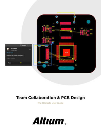
Transcription
High-Voltage PCB Design
HIGH-VOLTAGE PCB DESIGNHIGH VOLTAGE PCB DESIGNWhen it comes to designing high voltage PCBs, it's important to ensure your layout is able to control and optimize electric fieldstrengths for optimal operation and longevity. While the manufacturing process of high voltage PCBs remains similar to that ofnormal PCBs, careful attention to the materials you use, as well as their properties, are crucial to success. A thorough understandingof spacing rules, clearances, operating frequencies, and tried-and-true design techniques will go a long way in avoiding setbacks andpotential challenges.Join us as we explore topics about High Voltage PCB Design, including:How to Plan Your PCB Layout for a High Voltage DesignWhy Designing A High Voltage PCB for Rapid Prototyping is More Effective Than Rushing to Form FactorHigh Voltage PCB Design: Creepage and Clearance DistanceConsiderations for designing a high voltage PCBHigh Voltage PCB Design for Arc Prevention: How to Manage Pads and TracesHigh Voltage PCB Design Tips: Materials for High Voltage PCBswww.altium.com
HIGH-VOLTAGE PCB DESIGNHOW TO PLAN YOUR PCB LAYOUT FOR A HIGH VOLTAGE DESIGNI used to trail run with a friend who is an urban planner. As part of her devious plan to get me to run further before I was too tiredand bored, she’d tell me about the various considerations that go into the zoning and construction in a town. There were also a lot ofshenanigans with local politics that provided a juicy distraction.Although my friend would disagree, layouts for a high voltage PCB have some similarities to complex urban planning. In addition toall the other considerations that go into a PCB design, a high voltage PCB also needs a layout that can control and optimize fieldstrength across the board to provide the best performance and lifetime protection in your final product.ISOLATE HIGH VOLTAGE AREASThe same way that a town creates zoning areas and restricts what land can be used for, you want to group your high voltage circuitrytogether to minimize the impact it will have on the rest of your board. By partitioning high voltage areas from low voltage areas, youcan decrease the risk of arcing on your board.One way to physically isolate high voltage areas is to add an insert around them. When you lay out the board, be sure to include aslot that will be routered out where you’d place the insert. Talk to your manufacturer to be sure this is feasible, and to find out whatsize tolerance they have for the slot.www.altium.com
HIGH-VOLTAGE PCB DESIGNSince you are placing the slot near the highest voltage region of your board, overvoltage conditions are likely. Proto Expressrecommends that you design the slot to survive repeated arcing. The minimum slot width should provide adequate protection at thehighest voltage expected on the board. By adding a little margin to the slot size, you can ensure the PCB will stay undamaged even ifthe edges of the slot carbonize during corona or arcing. This is important because the resistance of the PCB material drops along theedges that suffer arc damage.During manufacturing, the slot will be routered like any other feature or via on the board. Then you can place an inert insulatormaterial into the slot to form a vertical barrier. For lower voltages, you can use PCB material, but at higher voltages, you’ll wantsomething like polyester or Teflon. The inserts can be held in place with clips, glue, or by designing the shape of the slot and insert tolock in place.Partitioning a high voltage PCB is important to provide a gradual decrease of voltage across the board.DECREASE VOLTAGE ACROSS THE BOARD GRADUALLYAfter you’ve isolated the highest voltage regions on the board, you should still lay out the rest of the board in “zones” that let youstep the voltage down gradually. By placing circuitry that operates at lower potential around the main conductors, you canredistribute the electric field. The lower field strength over an area lessens the potential for corona and arcing.Voltage floating rings, or field grating rings, can also be used to manage the field distribution of high voltage designs. They can serveas a termination or be coupled to resistors and/or capacitors, depending on the AC/DC characteristics of the high voltage sourcethat your design will protect. These are pretty advanced design components. If you’re considering using them, it is worth diving deepinto their literature.www.altium.com
HIGH-VOLTAGE PCB DESIGNISOLATE NOISE SOURCESIf there’s a single universal rule of PCB design it’s to either use short traces or isolate your noise sources. This is still the case whendesigning high voltage PCBs. Just like you don’t want to live next to a loud manufacturing plant, you don’t want signal or power noiseto reign-free on your board. If noise couples through parasitic capacitance on the board or in the insulation, it can easily propagateto very sensitive areas of the board.MINIMIZE INTERCONNECTSYou should minimize interconnects on your PCB. Using fewer interconnects reduces the opportunities for transient generation inyour design. It will also minimize the propagation of high voltage across the board. Like noise, any transients or unexpectedly highvoltage areas can damage sensitive components or reduce performance.PCB interconnects make it easier for the electric field to propagate across the board, which is highly undesirable.USE DESIGN CHECKSMake sure your PCB design tool has a thorough design rules checker. That checker is the urban planner of your board, making surethat spacing and positioning throughout the design and assembly of your board are up to spec. All cables, connectors, andcomponents can affect the performance of any board, but a high voltage product poses a particular risk to itself and users if thedesign goes awry.Looking for great design layout software for getting started? Look no further than Altium. Design rules checking can be automatedand performed in real time, saving you a tremendous amount of work in the small tweaks that are needed to get the board just right,especially for high voltage!www.altium.com
HIGH-VOLTAGE PCB DESIGNWHY DESIGNING A HIGH VOLTAGE PCB FOR RAPID PROTOTYPING ISMORE EFFECTIVE THAN RUSHING TO FORM FACTORRemember that fable we all were told as kids about the tortoise and the hare? The moral of the story was that slow and steady winsthe race. In engineering, this is especially true when it comes to creating a consumer product quickly. However, this practice is rarelythe approach we take. I personally experienced this when I rushed the design of a dimmer for the IOT market. In fact, I was makingtwo dimmers. The first dimmer was simpler and used a Triode for Alternating Current (TRIAC), and the second dimmer was morecomplicated and used a pair of high voltage Metal-Oxide Semiconductor Field-Effect Transistors (MOSFETs). Because the TRIACdimmer was simpler, I started with it and immediately went to a form factor design. Conversely, for the MOSFET dimmer, I didn’t rushto form factor. Instead, I left room for extra debugging because it was a much more difficult type of dimmer. This extra space allowedme to easily probe the underlying circuit. I call this technique “rapid prototyping” because it never produces an end product, butallows a designer to reach product milestones faster.Contrasting the development strategies of these dimmers is amazing. Both products released at nearly identical times despite theTRIAC dimmer being a simpler circuit and started several months prior to the MOSFET dimmer. The slowdown occurred becausegoing to form factor too early created many unanticipated issues later in the design process. As many of you know, a design is neveractually done until its specified requirements are met. The key to knowing a design is finished is being able to measure itsperformance to verify these requirements, and that is where we will start first.www.altium.com
HIGH-VOLTAGE PCB DESIGNTypical dimmer TRIAC and MOSFET componentsMAKING CRITICAL PERFORMANCE MEASUREMENTSIt was notoriously difficult to measure the performance metrics of the dimmer circuits, e.g., rise time, start up voltage, phase delay,etc. One major problem was the grounding method for the dimmer. The TRIAC used a full-wave bridge rectifier for the input to theAC/DC power supply, which meant that the system ground was not related to earth ground. As a result, we had to take extra care tonot destroy test equipment because of this. The form factor TRIAC PCB had very little room for probing or simulating an active circuit.Therefore, it could not be rigorously tested and instead relied on functional testing to validate its performance metrics. The MOSFETdimmer had many places to attach wires could and had many probe points so it could easily take advantage of an isolationtransformer to remove the grounding issue. Being able to test the dimmer was great, but it also meant that some aspects of thedesign needed to change once a failure was discovered. To test out ideas for solving these issues, the MOSFET PCB could havecomponents directly soldered to it because there was plenty of space and pads to do so. On the other hand, the TRIAC dimmerrequired a complete respin every time there was a change required because the spacing and size constraints were so tight.www.altium.com
HIGH-VOLTAGE PCB DESIGNExpanded PCB with debug headers, great for rapid prototypingMAKING CHANGES TO THE LAYOUT AND DESIGNOuch. Did you feel that? That’s the sting of having to deal with field failures or other issues reported during testing. It could also befrom the CEO wanting a new hot-rod feature that wasn’t previously scoped. The bottom line is that any true product design will gothrough several cycles for a whole multitude of reasons. These changes will be very costly if the layout is already form factored. Ahuge mistake I made was assuming a TRIAC didn’t have a polarity. The particular dimmer I was building could switch the LINE andLOAD terminals and still function correctly as a dimmer. This did not work at first because the TRIAC would not avalanche for one ofthese two directions. The only fix for this was adding another component to the PCB, which was extremely difficult in the form factordesign. A similar issue happened for the MOSFET design. The special voltage rail used to turn on the MOSFETs just wasn't goodenough and I needed to change the BUCK design that was part of the AC/DC circuit. In the non-form factor board all that took was avery quick and easy layout change to verify because space was not an issue at this point in the design cycle. However, you willeventually have to go to form factor.Brainstorming PCB layout changeswww.altium.com
HIGH-VOLTAGE PCB DESIGNYOU HAVE TO GO FORM FACTOR EVENTUALLYIt’s pretty clear that rushing to form factor can really slow a design down. Even so, a true design must go to form factor eventually.Even with state of the art PCB design software and inventory management systems, creating form factor designs takes a lot of work.That’s because it’s more than just planning a layout, it is also second sources for components and a real inventory managementsystem as production begins to ramp up. Any change to the layout that results in a Bill of Materials (BOM) change will have otherripple effects. The reality is that we will all rush to form factor at some point.If I hadn’t properly managed my TRIAC dimmer’s BOM throughout each revision then it would have taken even longer to go intoproduction. Remember, the components you initially sourced may no longer be available by the time you’re ready to send off yourdesigns to manufacturing, or the alternatives might not suit your budget. It’s common to forget about component availability whenyou’re focused on fixing design errors. While we have yet to automate PCB design, there is software that can track your components’availability and compare real-time pricing.Regardless of whether I’ve convinced you to follow my advice to try “rapid prototyping” or if you still prefer to go straight to formfactor, there are great bill of materials functions inside Altium software to help you out. I recommend using this PCB design softwareadd-on that can track component availability, obsolescence and compare pricing. Let the software handle your BOM so that you canfocus on your design.www.altium.com
HIGH-VOLTAGE PCB DESIGNHIGH VOLTAGE PCB DESIGN: CREEPAGE AND CLEARANCE DISTANCEWhen I was an undergrad, I did a lot of electrochemical etching. I put it on my resume for years, because interviewers were alwaysinterested in hearing about working with high voltage sources and terrifying chemicals. Later, I realized I didn’t want to be hired forjobs where they wanted someone with a pathological indifference to high-risk work environments.That was when I started looking into high voltage design. I was amazed by the standards that are required for high voltage products.I was also relieved. While I can’t prevent grad students from McGyvering our high voltage products, I do have peace of mind knowingthat there is board level protection in place.WHEN DOES SAFETY REQUIRE SPECIFIC SPACING RULES?Not every PCB design has the same rigorous rules on spacing that a high-voltage PCB design needs. In general, if the normaloperating voltage of your product meets or exceeds 30 VAC or 60 VDC, then you should be very diligent about spacing rules in yourboard design. If you have a high-density board, especially with high voltages, you need to be even more concerned. The high densitymakes spacing much trickier, and even more important for protection.Spacing is more important in high voltage designs because the voltage across your board makes it much easier for an arc to occurbetween two conductive elements on your PCB. Any arc that does occur poses a significantly higher risk to both the product andyour users. To help mitigate that risk, there are standards for two primary spacing measurements in your PCB design, clearance, andcreepage.www.altium.com
HIGH-VOLTAGE PCB DESIGNWHAT IS CLEARANCE?Clearance is the shortest distance through air between two conductors. I remember its definition by thinking of overhead clearance;how much room in the air before my head whacks into something. If the clearance anywhere on a PCB is too small, then an overvoltage event can cause an arc between neighboring conductive elements on the board.The rules for clearance vary with the PCB material, voltage, and environmental conditions. The environmental effects are prettysignificant. Most commonly, humidity changes the breakdown voltage of air and affects the likelihood of arcing. Dust is another factorsince particulates that collect on the surface of the PCB can form a track over time, shortening the distance between conductors.Arcing can damage your product and your users, so spacing on your board is a critical design parameter.WHAT IS CREEPAGE ON A PCB?Similar to clearance, creepage measures distance between conductors on a PCB. However, instead of measuring distance in air, itmeasures the shortest distance along the surface of the insulation material. Board material and environment also affect creepagerequirements. Moisture or particulate accumulation on the board can shorten creepage distance the same way they do forclearance.When you have a high density design, creepage can be a difficult requirement to meet. Since moving tracks is rarely the first choice,there are a couple other tricks for increasing the surface distance in your design. By adding either a slot between tracks, or a verticalbarrier of insulation, you can significantly increase the creepage distance without changing the trace layout on the board.www.altium.com
HIGH-VOLTAGE PCB DESIGNCONSIDER COMPARATIVE TRACKING INDEX (CTI) OF YOUR MATERIALAfter operating voltage, the most significant factor in the clearance and creepage requirements comes from the material propertiesof your PCB. The electrical insulation of the material is indicated by a “Comparative Tracking Index” or CTI value. The CTI is expressedas a voltage and is determined by a standardized test measuring when the surface of the material breaks down.There are six categories from 0 to 5 based on the breakdown value of the material. The mandatory insulation levels for products arebased on these CTI categories. Category 5 is the lowest, with values less than 100 V. With breakdowns of 600 V, Category 0 has themost robust, and often expensive, material options.PCB insulator materials have different breakdown voltages and corresponding safety categories for product applications.HOW DO I KNOW WHAT MATERIAL AND SPACING TO USE?Because there are so many variables in PCB design and material selection, your best bet for meeting the safety requirements andstandards is to go directly to the source. There are two standards I see referenced most often. The first is IPC-2221, which is thegeneric standard for guidance on PCB design clearance and creepage. The second is IEC-60950-1 (2nd edition). The IEC version isthe standard you want to read for any IT products with AC main or battery power, especially if you want to sell those productsinternationally.Since the consequences of incorrect spacing vary from legal non-compliance to serious death and destruction, it’s well worth thetime to become acquainted with any standards that are relevant to your design. Plus, it keeps the undergrads from zappingthemselves.Identifying and incorporating the standards can be time-consuming, so you should use a good design software. The best softwarefor PCB design lets you create specific design rules and helps you identify issues early in the process. Altium Designer fits theserequirements and more; you can get started designing even before you’ve chosen your board material!www.altium.com
HIGH-VOLTAGE PCB DESIGNCONSIDERATIONS FOR DESIGNING A HIGH VOLTAGE PCBI used to think that high voltage applications were only used in power engineering. Since I had no desire to work at a power plant ortransformer station, I was safe from having to learn high voltage PCB design. Alas, my interest in space applications proved me wrongand forced me to confront my laziness. It turns out high voltage applications show up in almost every industry, from manufacturingand power plants to medical and aerospace.Designing a PCB for high voltage applications requires consideration of a host of details at every level of your design and fabrication.The board will be subject to harsh operating conditions and will be much more sensitive to the lifetime of the parts and materials. Ifyou’re up for the challenge, then there are a few design considerations before you start your board layout.CONSIDER YOUR OPERATING FREQUENCYThe operating frequency of your product affects high voltage design as much as ESD and noise management affect the board. This isbecause high frequencies will arc at a lower voltage, requiring more stringent spacing around those signal lines.At the other end of the frequency spectrum, low voltage DC also needs special consideration. In certain environmental conditions, aDC differential can cause etching and electrochemical migration. While neither is desirable, electrochemical migration is the greaterrisk to performance and lifetime in high voltage designs. This is because conductor pads or traces will “grow” delicate, conductivefilaments, sometimes called whiskers, that can eventually create a short between potentials. At a minimum, they will create pointswww.altium.com
HIGH-VOLTAGE PCB DESIGNthat are more likely to arc, and decrease the effective creepage and clearance distances on your board.Electrochemical migration is most common with tin and silver, but even copper will occasionally produce those little filaments ofdestruction. To minimize your risk, don’t use pure tin or silver as a finish on your PCBs. If you’re using tin, even a low lead content isrecommended, as it will dramatically increase the difficulty of “growing” the conductive filaments.Many metals can grow whiskers. Tin whiskers tend to have a more 'fractalline' look.DERATE YOUR COMPONENTSWhen you are designing for high-stress environments, component tolerances will get “derated.” That means that you reduce thefunctional maximum value of the current, voltage, or temperature for a component or material to improve its lifetime in yourproduct. Often, it’s calculated simply by taking a percentage of the manufacturer rating. The percentage is usually specified by a MILSTD, or other specification determined by your customers and the operating environment for your product.In many cases, materials are derated to the average parameter value they are expected to experience, which makes for lessstringent requirements and cheaper production. However, the risk in high voltage designs comes from over-voltage events thatcause arcing or corona on the board. You should derate to the maximum voltage, rather than the average, to improve thesurvivability of your product during an over-voltage event.SELECT YOUR COMPONENTSAfter derating, you may find some of the initial components you’ve selected aren’t viable for your product’s operating environment.Even if they all pass, you should review each part again. The high voltage environment causes high variability in the electric fieldacross your PCB, but it also causes field stresses within individual components. To ensure the reliability of each component, SierraProto Express recommends that you have a minimum margin of 1.5:1, and possibly as high as 2:1.www.altium.com
HIGH-VOLTAGE PCB DESIGNIn some cases, the variability in voltage will not only damage the components but also cause them to become arc points for adischarge across the board. Component packaging should be considered carefully, since the cases and edges may have a sharpenough angle to concentrate the electric field. The same is true of any fasteners, clips, and connectors. Everything should have themaximum possible radius to distribute the electric field and avoid creating sites for over arc on your board.Casing and solder joints can concentrate the electric field on your PCB and increase the risk of over arc.Designing your PCB for high voltage applications is a particularly challenging task. However, the applications are so prevalent that it’shard to avoid ever working on a high voltage design. Fortunately, there is great PCB design software, like Altium Designer, that canhelp you manage design rules and get your board just right.www.altium.com
HIGH-VOLTAGE PCB DESIGNHIGH VOLTAGE PCB DESIGN FOR ARC PREVENTION: HOW TO MANAGEPADS AND TRACESGrowing up, I’d work obsessively on jigsaw puzzles with my grandmother. Like, skipping dinner obsessively. She was a grandmaster ofpuzzles; you only got to look at the picture once when you took the pieces out. If you needed more than your memory and patternrecognition, that was cheating. Instead of facing the shame of looking at the box, I learned to focus on the shapes of the pieces, andhow each fit with its neighbors. That way, not knowing the exact final picture was less paralyzing.Laying out traces and pads for a high voltage PCB design reminds me of doing jigsaw puzzles. You have an overall picture in yourmind, but the shape of each piece is still important if you want to get the final solution right. There are a couple different aspects toconsider for your pads and traces to get the shape just right, especially in high voltage applications.BEST PRACTICES FOR DESIGNING CORNERS ON YOUR HIGH VOLTAGECIRCUIT BOARDYou want to avoid any corners and sharp edges or turns on high voltage PCBs. For pads, use a smooth, round curve that cuts off thecorners. Design the curve with the largest radius you can without losing necessary surface area.www.altium.com
HIGH-VOLTAGE PCB DESIGNWhen you route the traces, you also want to avoid sharp corners at turns. Instead, use a curved track, again with the largest radiusyou’ve got space for.If you are using solder balls at connection points, you should also specify a minimum radius for the solder balls. Make sure youinform your manufacturer before they quote you for the fabrication, since you may need a larger solder ball than they typically use.Small radius solder balls can concentrate the electric field on a high voltage PCB and increase the risk of arcing or corona events.SPACING CONSIDERATIONS ON YOUR HIGH VOLTAGE CIRCUIT BOARDBy using curved edges instead of corners, you can use much a smaller spacing between features. According to Sierra Proto Board,direct arcing can occur at ⅓ the distance from a needlepoint as compared with a rounded edge. It’s also three times easier for aneedlepoint to generate corona.Sierra Proto also has equations to help you estimate your spacing distance based on your operating frequency. Remember that highfrequency will arc more easily, so your spacing increases by a recommended factor of 1.12X.Once you have your board, make sure that the surface and edges are clean, and all of the conductors are smooth before you powerit up. Dirt, rough edges, and scratches can all decrease the arc-over voltage by 70-80%BEST PRACTICES FOR DESIGNING EDGES ON YOUR HIGH VOLTAGECIRCUIT BOARDJust like edge pieces in a jigsaw puzzle, edges on a PCB will need special attention. When the edge of a board is machined orroutered, burrs are often left behind on the raw edge. If that happens on a conductive trace, the burr will function like a needlepointwww.altium.com
HIGH-VOLTAGE PCB DESIGNand dramatically increase the risk of arcing.To be safe, your layout should set copper traces back from any edges. Use a minimum buffer distance of 0.02 inches between aconductor and the edge. Increase the distance by 0.001 inches for every 100 V the trace will experience at its maximum load.Sometimes, you’ve got no choice but to shoehorn a trace in near the edge. In that case, you can use a conformal coat of a highvoltage compatible material, like HVPF. The coating allows you to provide additional protection to your PCB out to the edges of theboard.Traces and pads near the edge of a high voltage PCB require special design consideration to protect them from machining damage.My grandmother will disagree, but mistakes in a PCB design are much more serious than mistakes in a jigsaw puzzle. This is why youshould make sure that you’re using the best tools possible. An especially helpful feature in design software, like Altium Designer, issetting your own design rules. That way you don’t have to remember spacing distance and solder ball size while you’re optimizing alayout with only rounded tracks.Once you’ve put the puzzles away, Live support at Altium is available to help you learn more about how the best PCB software canhelp you improve your high voltage PCB design process.www.altium.com
HIGH-VOLTAGE PCB DESIGNHIGH VOLTAGE PCB DESIGN TIPS: MATERIALS FOR HIGH VOLTAGE PCBSAlong with designing electrical hardware and running for stress management, I’m an avid knitter. My grandmother taught me when Iwas in grade school, and I’ve taught a dozen or so people along the way. Before you can get to the fun part of actually knittingsomething, you have to select a yarn. Is it for a newborn? Then I want it to be soft, but also machine washable so the mom canactually use it without worrying about handwashing. Does it matter if it’s itchy? What if someone is allergic to wool? Does it need todrape or hold its shape?I have to sort through a surprising number of parameters before I can start knitting, or I’ll have to scrap everything and start freshwhen it doesn’t turn out well. The same is true when you select the materials for a PCB. Early in your PCB design career, you probablydidn’t specify much, and unless it was for a specialized project, it probably turned out fine. However, once you level up to highvoltage or other niche PCB applications, you need to start taking additional design requirements into consideration.SELECT AN APPROPRIATE PCB MATERIALThe foundation of your PCB is the board, so that’s the first material specification you should consider. You want the material to beappropriate for the performance requirements, but also for the operating environment since that will have a large impact on howthe PCB material ages.For a high voltage PCB, you’ll need a board material that’s specifically designed to tolerate an overvoltage event, as well as the regularwww.altium.com
HIGH-VOLTAGE PCB DESIGNhigh V operating conditions. There are a few material options you to consider:FR4 Laminate: FR4 high a very high dielectric breakdown. However, it is more porous than BT epoxy and polyimide, whichmakes it easier for the board to become contaminated. It also has a weak edge structure, and as the edge cracks, thedielectric value will decrease. Aging is a likely problem, especially for electronics near the edge. FR4 also has no recovery orprotection from carbonization that occurs during overvoltage events.BT Epoxy: A thermoset resin, BT epoxy has strong sidewalls and is better for applications with planar coils and mediumvoltage circuits.Isola, high V laminates: There are several high voltage laminates, Isola is one of the most well known, that actually extinguisharcs and leave a non-conductive base layer. While that is an incredible performance advantage in high V applications,understand the design restrictions before you start. These laminates are usually quite pricey, and you can only producesingle sided boards or very simple two sided boards.When you first start discussing production, get the datasheets for all your options from the manufacturer and make sure theperformance matches your requirements. Also, don’t mix and match the insulators on your board. The mismatch in materialproperties can cause issues in manufacturing and performance down the line.Don’t use multiple insulating materials within the layers of your PCB.CHECK GLASS AND RESIN CONTENTSIf the resin content and glass style us
HIGH-VOLTAGE PCB DESIGN www.altium.com HIGH VOLTAGE PCB DESIGN When it comes to designing high voltage PCBs, it's important to ensure your layout is able to control and optimize electric field strengths for optimal operation and longevity. While the manufacturing process of high voltage PCBs remains similar to that of