Transcription
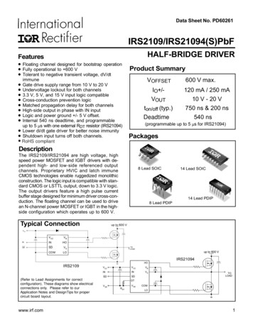
Data Sheet No. PD60261IRS2109/IRS21094(S)PbFHALF-BRIDGE DRIVERFeatures Floating channel designed for bootstrap operation Fully operational to 600 V Tolerant to negative transient voltage, dV/dtProduct SummaryVOFFSETimmune Gate drive supply range from 10 V to 20 V Undervoltage lockout for both channels 3.3 V, 5 V, and 15 V input logic compatible Cross-conduction prevention logic Matched propagation delay for both channels High-side output in phase with IN input Logic and power ground /- 5 V offset. Internal 540 ns deadtime, and programmableIO /VOUTton/off (typ.)Deadtime600 V max.120 mA / 250 mA10 V - 20 V750 ns & 200 ns540 ns(programmable up to 5 µs for IRS21094)up to 5 µs with one external RDT resistor (IRS21094) Lower di/dt gate driver for better noise immunity Shutdown input turns off both channels. RoHS compliantPackagesDescriptionThe IRS2109/IRS21094 are high voltage, highspeed power MOSFET and IGBT drivers with dependent high- and low-side referenced outputchannels. Proprietary HVIC and latch immuneCMOS technologies enable ruggedized monolithicconstruction. The logic input is compatible with standard CMOS or LSTTL output, down to 3.3 V logic.The output drivers feature a high pulse currentbuffer stage designed for minimum driver cross-conduction. The floating channel can be used to drivean N-channel power MOSFET or IGBT in the highside configuration which operates up to 600 V.Typical Connection8 Lead SOIC14 Lead SOIC14 Lead PDIP8 Lead PDIP IRS21094 IRS2109 (Refer to Lead Assignments for correctconfiguration). These diagrams show electricalconnections only. Please refer to ourApplication Notes and DesignTips for propercircuit board layout.www.irf.com T 1
IRS2109/IRS21094(S)PbFAbsolute Maximum RatingsAbsolute maximum ratings indicate sustained limits beyond which damage to the device may occur. All voltage parameters are absolute voltages referenced to COM. The thermal resistance and power dissipation ratings are measuredunder board mounted and still air conditions.SymbolDefinitionMin.Max.VBHigh-side floating absolute voltage-0.3625VSHigh-side floating supply offset voltageVB - 25VB 0.3VHOHigh-side floating output voltageVS - 0.3VB 0.3VCCLow-side and logic fixed supply voltage-0.325VLOLow-side output voltage-0.3VCC 0.3DTProgrammable deadtime pin voltage (IRS21094 only)VSS - 0.3VCC 0.3VINLogic input voltage (IN & SD)VSS - 0.3VCC 0.3VSSLogic ground (IRS21094/IRS21894 only)VCC - 25VCC 0.3dVS/dtAllowable offset supply voltage transientPDPackage power dissipation @ TA 25 C—50(8 Lead PDIP)—1.0(8 Lead SOIC)—0.625(14 lead PDIP)—1.6—1.0(8 Lead PDIP)—125(8 Lead SOIC)—200(14 lead PDIP)—75(14 lead SOIC)(14 lead SOIC)RthJAThermal resistance, junction to ambient—120TJJunction temperature—150TSStorage temperature-50150TLLead temperature (soldering, 10 seconds)—300www.irf.comUnitsVV/nsW C/W C2
IRS2109/IRS21094(S)PbFRecommended Operating ConditionsThe input/output logic timing diagram is shown in Fig. 1. For proper operation the device should be used within therecommended conditions. The VS and VSS offset rating are tested with all supplies biased at a 15 V differential.SymbolMin.Max.VBHigh-side floating supply absolute voltageDefinitionVS 10VS 20VSHigh-side floating supply offset voltage(Note 1)600VHOHigh-side floating output voltageVSVBVCCLow-side and logic fixed supply voltage1020VLOLow-side output voltage0VCCVINLogic input voltage (IN & SD)VSSVCCDTProgrammable deadtime pin voltage (IRS21094 only)VSSVCCVSSLogic ground (IRS21094 only)-55Ambient temperature-40125TAUnitsV CNote 1: Logic operational for VS of -5 V to 600 V. Logic state held for VS of -5 V to -VBS. (Please refer to the Design TipDT97-3 for more details).Dynamic Electrical CharacteristicsVBIAS (VCC, VBS) 15 V, VSS COM, C L 1000 pF, TA 25 C, DT VSS unless otherwise specified.SymbolDefinitiontonTurn-on propagation delaytofftsdTurn-off propagation delayMTShutdown propagation delayDelay matching, HS & LS turn-on/offMin.Typ.—750——Max. Units Test Conditions950VS 0 V200280VS 0 V or 600 V2 00280—070trTurn-on rise time—100220tfTurn-off fall time—358040054068056DTDeadtime: LO turn-off to HO turn-on(DTLO-HO) &HO turn-off to LO turn-on (DTHO-LO )MDTwww.irf.comDeadtime matching DTLO - HO - DTHO-LO4—060—0600nsVS 0 VRDT 0 ΩµsnsR DT 200 kΩ (IR21094)RDT 0 ΩRDT 200 kΩ (IR21094)3
IRS2109/IRS21094(S)PbFStatic Electrical CharacteristicsVBIAS (VCC, VBS) 15 V, VSS COM, DT VSS and TA 25 C unless otherwise specified. The VIL, VIH, and IINparameters are referenced to VSS /COM and are applicable to the respective input leads: IN and SD. The VO, IO, and Ronparameters are referenced to COM and are applicable to the respective output leads: HO and LO.SymbolDefinitionVIHLogic “1” input voltage for HO & logic “0” for LOVILMin. Typ. Max. Units Test Conditions2.5——Logic “0” input voltage for HO & logic “1” for LO——0.8VSD,TH SD input positive going threshold2.5——VSD,TH-SD input negative going threshold——0.8VOHHigh level output voltage, VBIAS - VO—0.050.2VOLLow level output voltage, VO—0.020.1ILKOffset supply leakage current——50IQBSQuiescent VBS supply current2075130IQCCQuiescent VCC supply current0.41.01.6IIN Logic “1” input bias current—520IIN-Logic “0” input bias �IO Output high short circuit pulsed current120290—IO-Output low short circuit pulsed current250600—VCCUV VBSUV VCCUVVBSUVVCCUVHVBSUVHwww.irf.comVCC and VBS supply undervoltage positive goingthresholdVCC and VBS supply undervoltage negative goingthresholdVCC 10 V to 20 VVIO 2 mAµAmAVB VS 600 VVIN 0 V or 5 VVIN 0 V or 5 VRDT 0 ΩIN 5 V, SD 0 VµAIN 0 V, SD 5 VVmAVO 0 V, PW 10 µsVO 15 V,PW 10 µs4
IRS2109/IRS21094(S)PbFFunctional Block MEUVDETECT ORVSS/CO ERATORVCCDEAD TIM EDTUVDETECT 5VSDQVSS/CO MLEVELSHIFTDELAYLOCO MVSSwww.irf.com5
IRS2109/IRS21094(S)PbFLead DefinitionsSymbol DescriptionINLogic input for high-side and low-side gate driver outputs (HO and LO), in phase with HO(referenced to COM for IRS2109 and VSS for IRS21094)Logic input for shutdown (referenced to COM for IRS2109 and VSS for IRS21094)SDDTProgrammable deadtime lead, referenced to VSS. (IRS21094 only)VSSLogic ground (IRS21094 only)VBHigh-side floating supplyHOHigh-side gate drive outputVSHigh-side floating supply returnVCCLow-side and logic fixed supplyLOLow-side gate drive outputCOMLow-side returnLead LOCOMLO541548 Lead PDIP8 Lead 87LO827www.irf.comVB214 Lead PDIP14 Lead SOICIRS21094PbFIRS21094SPbF6
ftr90%HOLOHOLOFigure 1. Input/Output Timing Diagramtf90%10%10%Figure 2. Switching Time Waveform Definitions50%50%INSD50%90%HOtsdHOLOLO90%DT LO-HO10%DT HO-LO90%10%MDT Figure 3. Shutdown Waveform DefinitionsDT LO-HO- DT HO-LOFigure 4. Deadtime Waveform DefinitionsIN (LO)50%50%IN (HO)LOHO10%MTMT90%LOHOFigure 5. Delay Matching Waveform Definitionswww.irf.com7
IRS2109/IRS21094(S)PbF1300Turn-On Propagation Delay (ns)Turn-On Propagation Delay (ns)13001100900M axTyp.700500-501100M ax.900Typ.700500-2502550751001251012Figure 6A. Turn-On Propagation Delayvs. Temperature161820Figure 6B. Turn-On Propagation Delayvs. Supply Voltage500Turn-Off Propagation Delay (ns)500Turn-Off Propagation Delay (ns)14VBIAS Supply Voltage (V)Temperature (oC)400300M ax.200Typ.100400M ax.300Typ.20010000-50-250255075100125oTemperature ( C)Figure 7A. Turn-Off Propagation Delayvs. Temperaturewww.irf.com101214161820V BIAS Supply Voltage (V)Figure 7B. Turn-Off Propagation Delayvs. Supply Volta ge8
IRS2109/IRS21094(S)PbF500SD Propagation Delay (ns)SD Propagation Delay (ns)500400300M ax.200Typ.100400M re ( C)Figure 8A. SD Propagation Delayvs. Temperature161820Figure 8B. SD Propagation Delayvs. Supply Voltage50 0Turn-On(ns)T urn-O n RiseR is e TTimeim e (ns)5 00T urn-O n RRiseis e TTimeim e (ns(ns))Turn-On14V BIAS Supply Voltage (V)o4 003 002 00Max.1 00Typ.040 030 0Max.20 0Typ.10 00-5 0-2 502550751 00Temperature(oC)Figure 9A. Turn-On Rise Timevs. Temperaturewww.irf.com1 25101214161820VBIAS Supply Voltage (V)Figure 9B. Turn-On Rise Timevs. Supply Volta ge9
IRS2109/IRS21094(S)PbF200T u rn-O ffTimeF allT(ns)im eTurn-OffFallTurn-Off Fall Time (ns)2 001 501 00Max.50Typ.0150100Max.50Typ.0-5 0-2 502550751 001 251012Temperature(oC)1820Figure 10B. Turn-Off Fall Timevs. Supply Voltage10001000800800Deadtime (ns)Deadtime (ns)16Input Voltage (V)Figure 10A. Turn-Off Fall Timevs. TemperatureM ax.600Typ.40014M in.600M ax.Typ.M in.400200200-50-250255075100125oTemperature ( C)Figure 11A. Deadtime vs. Temperaturewww.irf.com101214161820V BIAS Supply Voltage (V)Figure 11B. Deadtime vs. Supply Voltage10
IRS2109/IRS21094(S)PbF57Input Voltage (V)6Deadtime( s)Deadtime(µs)M ax.5Typ.4M in.3243Min.211-500050100150200-250R(kΩ)RDTDT (KΩ)3Min.211618VBIAS Supply Voltage (V)Figure 12B. Logic “1” Input Voltagevs. Supply Voltagewww.irf.com20Logic "0" Input Bias Current (µA)Input Voltage (V)41475100125Figure 12A. Logic “1” Input Voltagevs. Temperature51250Temperature (oC)Figure 11C. Deadtime vs. R DT(IR21094 only)102565Max43210-50-250255075100125Temperature ( C)Figure 13A. Logic "0" Input Bias Currentvs. Temperature11
565SD Input threshold ( ) (V)Logic "0" Input Bias Current (µA)IRS2109/IRS21094(S)PbFMax4321010121416182043 Max.210-50-25Supply Voltage (V)255075100125oTemperature ( C)Figure 13B. Logic "0" Input Bias CurrentFigure 14A. SD Input Positive GoingThreshold ( ) vs. Temperaturevs. Voltage55SD Negative Going Threshold (V)SD Input threshold ( ) (V)043Max.210101214161820VCC Supply Voltage (V)Figure 14B. SD Input Positive Going Threshold ( )vs. Supply Voltagewww.irf.com432M in.10-50-250255075100125oTemperature ( C)Figure 15A. SD Negative Going Thresholdvs. Temperature12
IRS2109/IRS21094(S)PbFHigh Level Output Voltage (V)SD Negative Going Threshold (V)5432M in.101012141618200.50.40.30.2Max.0.1Typ.0.0-50-25V CC Supply Voltage (V)Low Level Output Voltage (V)High Level Output Voltage (V)0.4Max.0.20.1Typ.0.012141618VBIAS Supply Voltage (V)Figure 16B. High Level Output Voltagevs. Supply Volta gewww.irf.com5075100125Figure 16A. High Level Output Voltagevs. Temperature0.51025Temperature (oC)Figure 15B. SD Negative Going Thresholdvs. Supply Volta 125Temperature (oC)Figure 17A. Low Level Output Voltagevs. Temperature13
pplySupplyLeakageLeakageCurrentCurrent(µA)( A)Low Level Output Voltage (V)IRS2109/IRS21094(S)PbF500400300200100M ax.0-50-25255075100125oVBIAS Supply Voltage (V)Temperature ( C)Figure 17B. Low Level Output Voltagevs. Supply VoltageFigure 18A. Offset Supply Leakage Currentvs. Temperature500400V BSS u p p ly C u rre n t ( A )VBS Supply Current (µA)OOffsetffs e t SSupplyu p p ly LLeakagee a ka g e CCurrentu rre n t ( (µA)A)0400300200100M ax.300200M ax.100Typ.M in.000100200300400500600VB Boost Voltage (V)Figure 18B. Offset Supply Leakage Currentvs. Boost Voltagewww.irf.com-50-250255075100125Temperature (oC)Figure 19A. VBS Supply Currentvs. Temperature14
IRS2109/IRS21094(S)PbF3.02.5VCC Supply Current (mA)VBS Supply Current (µA)400300200M ax.100Typ.2.0M ax.1.5Typ.1.0M in.0.5M in.00.0101214161820-50-25Figure 19B. VBS Supply Currentvs. Supply Voltage255075100125Figure 20A. V CC Supply Currentvs. Temperature3.060Logic "1" Input Current (µA )V CC Supply Current (mA)0Temperature (oC)VBS Supply Voltage (V)2.52.01.5M ax.1.0Typ.0.5M in.5040302010M ax.Typ.0.001012141618V CC Supply Voltage (V)Figure 20B. VCC Supply Currentvs. VCC Supply Voltagewww.irf.com20-50-250255075100125Temperature ( oC)Figure 21A. Logic “1” Input Currentvs. Temperature15
IRS2109/IRS21094(S)PbF5Logic 0”"0"InputInput CurrentCurrent (µA)( A)Logic “1”"1" InputInput Current ((µA)A)Logic60504030M ax.2010Typ.43M ax.2010101214161820-50-250V CC Supply Voltage (V)5075100125oTemperature ( C)Figure 21B. Logic “1” Input Currentvs. Supply VoltageFigure 22A. Logic “0” Input Currentvs. Temperature12V CC UVLO Threshold ( ) (V)5LogicA)Logic"0"0” Input CurrentCurrent ((µA)2543M ax.211110M ax.9Typ.M in.8701012141618V CC Supply Voltage (V)Figure 22B. Logic “0” Input Currenttvs. Supply e ( C)Figure 23. VCC Undervoltage Threshold ( )vs. Temperature16
IRS2109/IRS21094(S)PbF12V BS UVLO Threshold ( ) (V)V CC UVLO Threshold (-) (V)1110M ax.9Typ.8M in.7611M ax.10Typ.9M in.87-50-250255075100125-50-250Temperature ( oC)Figure 24. V CC Undervoltage Threshold (-)vs. Temperature5075100125Figure 25. VBS Undervoltage Threshold ( )vs. Temperature500Output Source Current (mA)11V BS UVLO Threshold (-) (V)25Temperature ( oC)10M ax.9Typ.8M rature (oC)Figure 26. V BS Undervoltage Threshold (-)vs. re (oC)Figure 27A. Output Source Currentvs. Temperature17
IRS2109/IRS21094(S)PbF1000Output Sink(µA)OutputSinkCurrentCurrent(mΑ)Output SourceSource BIAS Supply Voltage (V)Temperature (oC)Figure 27B. Output Source Currentvs. Supply VoltageFigure 28A. Output Sink Currentvs. Temperature1250V S Offset Supply Voltage (V)1000OutputCurrent(mΑ)Output SinkSink 101012141618VBIAS Supply Voltage (V)Figure 28B. Output Sink Currenttvs. Supply Voltagewww.irf.com20101214161820V BS Flouting Supply Voltage (V)Figure 29. Maximum V S Negative Offsetvs. Supply Voltage18
140140120120100140 V8070 V600 VTemperature (oC)Temperature (oC)IRS2109/IRS21094(S)PbF40100140 V8070 V600 V40202011010011000Figure 30. IRS2109 vs Frequency (IRFBC20)Rgate 33 Ω, VCC 15 V1000Figure 31. IRS2109 vs Frequency (IRFBC30)Rgate 22 Ω, VCC 15 V140140120120140 V8070 V600V40Temperature (oC)Temperature ( oC)100Frequency (kHz)Frequency (kHz)10010140 V 70 V0V10080604020201101001000Frequency (kHz)Figure 32. IRS2109 vs Frequency (IRFBC40)Rgate 15 Ω, VCC 15 Vwww.irf.com1101001000Frequency (kHz)Figure 33. IRS2109 vs Frequency (IRFPE50)Rgate 10 Ω, VCC 15 V19
1401401201201008060140 VTemperature (oC)Temperature (oC)IRS2109/IRS21094(S)PbF10080140 V6070 V70 V0 V40400 V202011010011000101001000Frequency (kHz)Frequency (kHz)Figure 35. IRS21094 vs. Frequency (IRFBC30),Rgate 22 Ω , V CC 15 VFigure 34. IRS21094 vs. Frequency (IRFBC20),Rgate 33 Ω , V CC 15 V140140120120140 V100140 V8070 V0 V60Temperature (oC)Temperature (oC)70 V1008060404020201101001000Frequency (kHz)Figure 36. IRS21094 vs. Frequency (IRFBC40),Rgate 15 Ω , VCC 15 Vwww.irf.com0 V1101001000Frequency (kHz)Figure 37. IRS21094 vs. Frequency (IRFPE50),Rgate 10 Ω , V CC 15 V20
IRS2109/IRS21094(S)PbF14014012012010080140 V70 V600 VTemperature (oC)Temperature (oC)140 V4010070 V0 V80604020201101001000110Frequency (kHz)Figure 39. IRS2109S vs. Frequency (IRFBC30),Rgate 22 Ω , V CC 15 V140 V 70 V140 V 70 V 0 V1401200 V1008060Tempreture (oC)120Temperature (oC)1000Frequency (kHz)Figure 38. IRS2109S vs. Frequency (IRFBC20),Rgate 33 Ω , V CC 15 V1401001008060404020201101001000Frequency (kHz)Figure 40. IRS2109S vs. Frequency (IRFBC40),Rgate 15 Ω , V CC 15 Vwww.irf.com1101001000Frequency (kHz)Figure 41. IRS2109S vs. Frequency (IRFPE50),Rgate 10 Ω , V CC 15 V21
1401401201201008060140 V70 V0V40Temperature (oC)Temperature (oC)IRS2109/IRS21094(S)PbF80140 V70 V600V40202011010011000101001000Frequency (kHz)Frequency (kHz)Figure 42. IRS21094S vs. Frequency (IRFBC20),Rgate 33 Ω, Vcc 15 VFigure 43. IRS21094S vs. Frequency (IRFBC30),Rgate 22 Ω, Vcc 15 V140140120120100140 V70 V800 V60Temperature (oC)Temperature (oC)100140 V 70 V0 V10080604040202011101001000101001000Frequency (kHz)Frequency (kHz)Figure 44. IRS21094S vs. Frequency (IRFBC40),Rgate 15 Ω, Vcc 15 Vwww.irf.comFigure 45. IRS21094S vs. Frequency (IRFPE50),Rgate 10 Ω, Vcc 15 V22
IRS2109/IRS21094(S)PbFCase Outlines01-601401-3003 01 (MS-001AB)8 Lead PDIPDDIMB5AFOOTPRINT86765HE1230.25 [.010]4A6.46 [.255]MIN.0532.06881.351.75A1 .0040e3X 1.27 190.25D.189.19684.805.00E.1497.15743.804.00e.050 BASIC0.25 [.010]A10.635 500.401.27y0 8 0 8 y0.10 [.004]8X L8X c7C A BNOTES:1. DIMENSIONING & TOLERANCING PER ASME Y14.5M-1994.2. CONTROLLING DIMENSION: MILLIMETER3. DIMENSIONS ARE SHOWN IN MILLIMETERS [INC HES].4. OUTLINE CONFORMS TO JEDEC OUTLINE MS-012AA.8 Lead SOICwww.irf.com.025 BASIC1.27 BASICK x 45 AC8X b8X 1.78 [.070]MAXbe16XMILLIMETERSMAXA8X 0.72 [.028]INCHESMIN5 DIMENSION DOES NOT INCLUDE MOLD PROTRUSIONS.MOLD PROTRUSIONS NOT TO EXCEED 0.15 [.006].6 DIMENSION DOES NOT INCLUDE MOLD PROTRUSIONS.MOLD PROTRUSIONS NOT TO EXCEED 0.25 [.010].7 DIMENSION IS THE LENG TH OF LEAD FOR SOLDERING TOA SUBSTRATE.01-602701-0021 11 (MS-012AA)23
IRS2109/IRS21094(S)PbF14 Lead PDIP14 Lead SOIC (narrow body)www.irf.com01-601001-3002 03 (MS-001AC)01-601901-3063 00 (MS-012AB)24
IRS2109/IRS21094(S)PbFTape & Reel8-lead SOICLOAD ED TA PE FEED DIRECTIONABHDFCN OTE : CO NTROLLINGD IMENSION IN M MEGC A R R I E R T A P E D IM E N S I O N F O R 8 S O I C NM etr icIm p e r i a lCod eM inM axM inM axA7 .9 08 .1 00 . 31 10 .3 1 8B3 .9 04 .1 00 . 15 30 .1 6 1C1 1 .7 01 2.300 .4 60 .4 8 4D5 .4 55 .5 50 . 21 40 .2 1 8E6 .3 06 .5 00 . 24 80 .2 5 5F5 .1 05 .3 00 . 20 00 .2 0 8G1 .5 0n/ a0 . 05 9n/ aH1 .5 01 .6 00 . 05 90 .0 6 2FDCBAEGHR E E L D IM E N S I O N S F O R 8 S O IC NM etr icIm p e r i a lCod eM inM axM inM axA3 2 9. 6 03 3 0 .2 51 2 .9 7 61 3 .0 0 1B2 0 .9 52 1.450 . 82 40 .8 4 4C1 2 .8 01 3.200 . 50 30 .5 1 9D1 .9 52 .4 50 . 76 70 .0 9 6E9 8 .0 01 0 2 .0 03 . 85 84 .0 1 5Fn /a1 8.40n /a0 .7 2 4G1 4 .5 01 7.100 . 57 00 .6 7 3H1 2 .4 01 4.400 . 48 80 .5 6 6www.irf.com25
IRS2109/IRS21094(S)PbFTape & Reel14-lead SOICLOAD ED TA PE FEED DIRECTIONABHDFCN OTE : CO NTROLLINGD IMENSION IN M MEGC A R R I E R T A P E D IM E N S I O N F O R 1 4 S O IC NM etr icIm p e r i a lCod eM inM axM inM axA7 .9 08 .1 00 . 31 10 .3 1 8B3 .9 04 .1 00 . 15 30 .1 6 1C1 5 .7 01 6.300 . 61 80 .6 4 1D7 .4 07 .6 00 . 29 10 .2 9 9E6 .4 06 .6 00 . 25 20 .2 6 0F9 .4 09 .6 00 . 37 00 .3 7 8G1 .5 0n/ a0 . 05 9n/ aH1 .5 01 .6 00 . 05 90 .0 6 2FDCBAEGHR E E L D IM E N S I O N S F O R 1 4 S O IC NM etr icIm p e r i a lCod eM inM axM inM axA3 2 9. 6 03 3 0 .2 51 2 .9 7 61 3 .0 0 1B2 0 .9 52 1.450 . 82 40 .8 4 4C1 2 .8 01 3.200 . 50 30 .5 1 9D1 .9 52 .4 50 . 76 70 .0 9 6E9 8 .0 01 0 2 .0 03 . 85 84 .0 1 5Fn /a2 2.40n /a0 .8 8 1G1 8 .5 02 1.100 . 72 80 .8 3 0H1 6 .4 01 8.400 . 64 50 .7 2 4www.irf.com26
IRS2109/IRS21094(S)PbFLEADFREE PART MARKING INFORMATIONIRxxxxxxSPart numberYWW?Date codePin 1Identifier?PMARKING CODELead Free ReleasedNon-Lead FreeReleasedIR logo?XXXXLot Code(Prod mode - 4 digit SPN code)Assembly site codePer SCOP 200-002ORDER INFORMATION8-Lead PDIP IRS2109PbF8-Lead SOIC IRS2109SPbF8-Lead SOIC Tape & Reel IRS2109STRPbF14-Lead PDIP IRS21094PbF14-Lead SOIC IRS21094SPbF14-Lead SOIC Tape & Reel IRS21094STRPbFSOIC8 &14 are MSL2 qualified.This product has been designed and qualified for the industrial level.Qualification standards can be found at www.irf.comIR WORLD HEADQUARTERS: 233 Kansas St., El Segundo, California 90245, USA Tel: (310) 252-7105Data and specifications subject to change without notice. 12/4/2006www.irf.com27
IRS2109/IRS21094(S)PbF www.irf.com 2 Symbol Definition Min. Max. Units VB High-side floating absolute voltage -0.3 625 VS High-side floating supply offset voltage VB - 25 VB 0.3 VHO High-side floating output voltage VS - 0.3 VB 0.3 VCC Low-side and logic fixed supply voltage -0.3 25 VLO Low-side output voltage -0.3 VCC 0.3 DT Programmable deadtime pin voltage (IRS21094 only) VSS - 0.3 .