Transcription
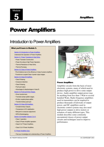
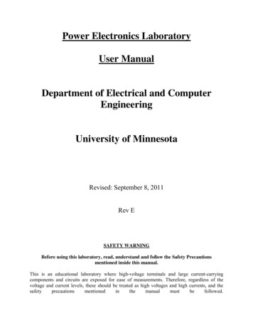
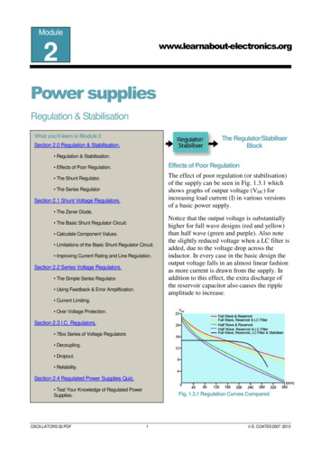
Module2www.learnabout-electronics.orgPower suppliesRegulation & StabilisationWhat you’ll learn in Module 2The Regulator/StabiliserBlockSection 2.0 Regulation & Stabilisation. Regulation & Stabilisation.Effects of Poor Regulation Effects of Poor Regulation.The effect of poor regulation (or stabilisation)of the supply can be seen in Fig. 1.3.1 whichshows graphs of output voltage (VDC) forincreasing load current (I) in various versionsof a basic power supply. The Shunt Regulator. The Series RegulatorSection 2.1 Shunt Voltage Regulators. The Zener Diode. The Basic Shunt Regulator Circuit. Calculate Component Values. Limitations of the Basic Shunt Regulator Circuit. Improving Current Rating and Line Regulation.Section 2.2 Series Voltage Regulators. The Simple Series Regulator. Using Feedback & Error Amplification.Notice that the output voltage is substantiallyhigher for full wave designs (red and yellow)than half wave (green and purple). Also notethe slightly reduced voltage when a LC filter isadded, due to the voltage drop across theinductor. In every case in the basic design theoutput voltage falls in an almost linear fashionas more current is drawn from the supply. Inaddition to this effect, the extra discharge ofthe reservoir capacitor also causes the rippleamplitude to increase. Current Limiting. Over Voltage Protection.Section 2.3 I.C. Regulators. 78xx Series of Voltage Regulators Decoupling. Dropout. Reliability.Section 2.4 Regulated Power Supplies Quiz. Test Your Knowledge of Regulated PowerSupplies.OSCILLATORS 02.PDFFig. 1.3.1 Regulation Curves Compared1 E. COATES 2007 -2013
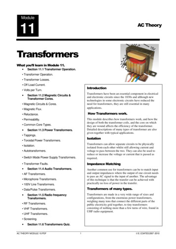
www.learnabout-electronics.orgRegulation & StabilisationRegulator (Stabiliser)These problems can be largely overcome byincluding a regulator stage at the power supplyoutput. The effect of this circuit can be seen inFig. 1.3.1. as the black line on the graph, wherefor any current up to about 200mA the outputvoltage (although lower than the absolutemaximum provided by the basic supply) remainsconstant.A regulator counteracts the effects of varyingload current by automatically compensating forthe reduction in output voltage as currentincreases.It is also common in regulated supplies, that theoutput voltage is automatically and suddenlyreduced to zero as a safety measure if the currentdemand exceeds a set limit. This is called CurrentLimiting.Regulator or Stabiliser?Strictly speaking, compensating forvariations in the mains (line) input voltageis called REGULATION, whilecompensating for variations in load currentis called STABILISATION. In practice youwill find these terms used rather loosely todescribe compensation for both effects. Infact most stabilised or regulated powersupplies compensate for both input andoutput variations and so are both (at least tosome degree) stabilised and regulated powersupplies.In common with much modern usage, theterm ‘Regulator’ will be used here todescribe both regulation and stabilisation.Regulation requires extra circuitry at the output of a simple power supply. The circuits used varygreatly in both cost and complexity. Two basic forms of regulation are used:1. The shunt regulator.2. The series regulator.These two approaches are compared in Fig. 1.3.2 & Fig 1.3.3The Shunt RegulatorIn the shunt regulator (Fig. 1.3.2) , a circuitis connected in parallel with the load. Thepurpose of the regulator is to ensure a stablevoltage across the load at all times; this isachieved by arranging that a current willflow through the regulator circuit at alltimes. If the load current increases, then theregulator circuit reduces its current so thatthe total supply current IT, (made up of theload current IL plus the regulator current IS),remains at the same value. Similarly if theload current decreases, then the regulatorcurrent increases to maintain a steady totalcurrent IT. If the total supply current remainsthe same, then so will the supply voltage.POWER SUPPLIES MODULE 02.PDFFig. 1.3.2 The Shunt Regulator2 E. COATES 2007-2016
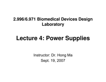
www.learnabout-electronics.orgRegulation & StabilisationThe Series RegulatorIn the series regulator (Fig. 1.3.3), thecontrolling device is in series with the load.At all times there will be a voltage dropacross the regulator. This drop will besubtracted from the supply voltage to give avoltage VL across the load, which is thesupply voltage VT minus the regulatorvoltage drop VS. Therefore:VL VT - VSFig. 1.3.2 The Series RegulatorSeries regulators are usually controlled by a sample of the load voltage, using a negative feedbacksystem. If the load voltage tends to fall, the smaller feedback causes the controlling device to lessenits resistance, allowing more current to flow into the load, so increasing the load voltage to itsoriginal value. An increase in load voltage will have the opposite effect. Like shunt regulation, theaction of the series regulator will also compensate for variations in the supply voltage.POWER SUPPLIES MODULE 02.PDF3 E. COATES 2007-2016
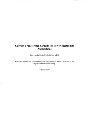
www.learnabout-electronics.orgRegulation & Stabilisation2.1 Shunt Voltage RegulatorsWhat you’ll learn in Module 2.1After studying this section, you should beable to:Understand the principles of shunt regulators. Regulating action of a zener diode. Operation of the basic shunt regulatorcircuit. Calculate component values for a basicshunt regulator circuit.Recognise the limitations of the basic shuntregulator.Understand methods for increasing currentrating.Recognise cascading techniques forimproving line regulation.Basic Shunt RegulatorCircuitsShunt regulators are widelyused because they are cheap,effective and simple. It isunusual however, to find ashunt regulator used as themain regulating circuit in alarge power supply. Shuntregulation is only reallyFig. 2.1.1 Basicsuitable, at reasonable cost,ShuntRegulatorfor relatively small currentsand a range of fixed, usuallyfairly low voltages. As mentioned in power suppliesmodule 2.0, a regulation current must always beflowing in addition to the load current. This is wastefulof power if large currents are involved.The basic shunt regulator circuit is shown in Fig. 2.1.1 and consists of only two components; aseries resistor RS feeding current to a zener diode, which is connected in reverse polarity) across theload.The Zener Diode.The main property of a zener diode is that thevoltage across the diode (VZ) will remainpractically steady for a wide range of current(IZ) when the diode is operated in reverse biasmode, as shown in Fig. 2.0.1.Fig. 2.1.2 illustrates the characteristic curve ofa zener diode where the operating region(shown in green) of the zener diode is a rangeof current on the nearly vertical breakdownregion of the curve.Provided that the reverse current is kept at avalue above about 1 to 2mA (avoiding the"knee" of the reverse characteristic) and doesnot exceed the safe working current for thatparticular diode type, very little change inreverse voltage takes place. It is this effectthat is used to give the required regulating effect.Fig. 2.1.2 Zener Diode Characteristic CurveAs the power supply operates, two conditions may occur to change the output voltage;a. The load current may vary.b. The supply voltage may vary.POWER SUPPLIES MODULE 02.PDF4 E. COATES 2007-2016
www.learnabout-electronics.orgRegulation & StabilisationThe circuit is arranged so that the total supply current IS is made up of the output load current IOUTplus the current in the zener diode IZ:IS IZ IOUTProvided that the zener diode is working within its allowable range of current, the voltage VZ willremain practically constant, deviating by only a very small amount (δV).Point of Load RegulatorsThe most common method of using these basic zener diode shunt regulators is the ‘point of load’regulation system. This method uses a number of fixed voltage, relatively low current regulators atvarious points around the circuit being supplied.A relatively ineffective main regulator can thenbe used in the power supply unit because eachsection of the circuit has its own regulator. Forexample many complex circuits need differentvoltage levels for different electrical andelectromechanical parts. Each may have its ownregulated supply, e.g. 9V, 5V or 3.3V, using"point of load" shunt regulators fed from asingle common supply, as shown in Fig. 2.1.3.Each of the voltage regulators will normally beplaced as close to the circuit supplied asphysically possible, and have additionaldecoupling capacitors to reduce any noise orcross talk between the individual supply lines.Fig. 2.1.3 Point of Load RegulatorsVariations in Load CurrentIf the current in the load Iout tends to fall, the voltage across the load would tend to rise, butbecause it is connected in parallel with the diode the voltage will remain constant. What will changeis the current (IZ) through the diode. This will rise by an amount equal to the fall of current in theload. The total supply current IS being always equal to IZ IOUT. An increase in load current IOUTwill likewise cause a fall in zener current IZ, again keeping VZ and the output voltage steady.Variations in Input VoltageIf the input voltage rises this will cause more supply current IS to flow into the circuit. Without thezener shunt regulator, this would have the effect of making the output voltage Vout rise, but anytendency for VOUT to rise will simply cause the diode to conduct more heavily, absorbing the extrasupply current without any increase in VZ thus keeping the output voltage constant. A fall in theinput voltage would likewise cause a reduction in zener current, again keeping VOUT steady.LimitationsThis simple shunt regulator is only suitable for relatively small currents and a fixed range ofvoltages. There are a number of limitations to the use of this circuit:Output voltage:The output voltage is equal to the zener voltage of the diode and so is fixed at one of the availablevoltage levels.POWER SUPPLIES MODULE 02.PDF5 E. COATES 2007-2016
www.learnabout-electronics.orgRegulation & StabilisationOutput current:If the output current falls to zero for any reason (the load may become open circuit due to a fault, orbe disconnected from the power supply), all of the load current must be passed by the zener diode.Therefore the maximum current available for the load must be no greater than the maximum safecurrent for the zener diode alone.Input voltage:The input voltage must be higher (usually about 30% higher) than the output voltage to allowregulation to take place. It should not be too high however, as this will result in more power beingdissipated by the diode.Power dissipation:The power dissipated in the diode must be kept within the safe working limits for the device chosen.Maximum power will be dissipated if the load is allowed to go open circuit while the input voltageis at its maximum value. This ‘worst case’ should not exceed the diode‘s maximum power rating.The above limitations are controlled by the suitable choice of zener diode and series resistor RS.The design of simple regulator circuits is fairly straightforward if a few simple steps are followed:1. Decide on a zener diode of the required voltage.2. Select a diode whose maximum current at least matches, and preferably exceeds the maximumcurrent requirement of the load.Note: Zener diode ratings usually quote maximum power dissipation rather than current, so youwill need to work out the current rating from the power and voltage given for the device.3. Find out the highest voltage likely to occur at the supply input. (VIN max)4. Calculate the value of a suitable series resistor RS by using the formula:Where:VIN max the highest likely input voltage.VZ the zener diode voltageIOUT max the maximum output current.IZ min the minimum current at which the zener will operate (say about 1 to 2mA).5. Calculate the power dissipated in the series resistor (RS) by the formula:Power dissipated by RS VR x IINNote: When calculating power ratings and resistances, your answers will probably not exactlymatch the commercially available preferred values. Therefore choose the closest preferred value,and then put this value into your calculations to make sure the circuit will operate correctly with thepreferred value. You should then be able to quote:A suitable resistor value and its power rating and a suitable zener diode type number.POWER SUPPLIES MODULE 02.PDF6 E. COATES 2007-2016
www.learnabout-electronics.orgRegulation & StabilisationExample:Design a simple zener diode (see Fig. 2.1.4) shunt regulator circuit with thefollowing specifications:Maximum load current required. 100mAOutput voltage. 12VInput voltage. 15V nominal, 16V max.Assuming a minimum zener current of 1mAFig. 2.1.4 ExampleThe problem can be solved in 4 steps.1. Find a value for RSRS must supply sufficient current to keep IZ at or slightly above 1mA when the zener diodeis passing its minimum current.As the total circuit current IIN IOUT IZThe minimum zener diode current will occur when the input voltage (VIN) is at its minimumvalue and the load current (IOUT) is at its maximum value.Under these conditions the current (IIN) flowing through RS will be IOUT max IZ minWhich is 100mA 1mA 101mAAs R V/I and the voltage across RS VIN min - VZThen RS (VIN min - VZ)/IIN (15 -12) / 101exp-3 29.7ΩTherefore a practical value for RS will be the next lowest preferred value 27Ω)2. Calculate the maximum current (IIN max) that will pass through RS.The maximum current (IIN max) will occur when VIN is at nits maximum value, i.e. 16VIIN max (VIN max - VZ) / RS (16 - 12) / 27 4 / 27 148mA3. Calculate the maximum power requirement for RSThis will occur when VIN is at its maximum value).(VIN max - VZ) x IIN max (16 - 12) x 148exp-3 0.592WA practical power rating for RS will therefore be the next highest available power rating 1W)4. Calculate the maximum power (PZ max) that must be dissipated by the zener diode.This will be the power that the zener diode would need
POWER SUPPLIES MODULE 02.PDF 6 E. COATES 2007-2016 Output current: If the output current falls to zero for any reason (the load may become open circuit due to a fault, or be disconnected from the power supply), all of the load current must be passed by the zener diode. Therefore the maximum current available for the load must be no greater than the maximum safe current for the