Transcription
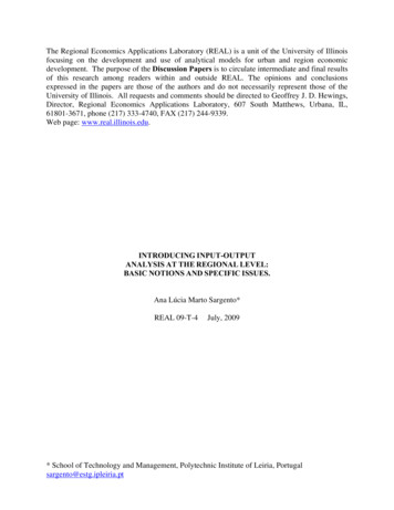
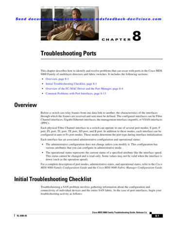
2015-10-17Input/Output portsATmega32Erasmus 2015/2016, WIEiK, PKMicrocontrollerPower Supplyclockfx(Central Proccesor Unit)HardwareInterruptssystemIRQInternal address busInternal data busInternal control busResetCPUProgram memoryROMData memoryRAMBasic Input/OutputDevices Parallel Port Serial Port CountersGeneral purposeInput/output portsMicrocontroller – all components of computer system in one an integrated circuit (chip)Erasmus 2015/2016, WIEiK, PK1
2015-10-17Input/output devices In computing, input/output or I/O is the communication between an computer systemand the outside world, possibly a human or another information processing system. Inputs are the signals or data received by the system, and outputs are the signals or datasent from it. The term can also be used as part of an action; to "perform I/O" is to perform an inputor output operation. I/O devices are used by a person (or other system) to communicate with a computer. For instance, a keyboard or a mouse may be an input device for a computer, while LEDdiodes, displays , monitors and printers are considered output devices for a computer. All microntrollers contain I/O ports to allow data to be read from switches, sensors etc.and to write to LED’s, LCD displays, motors etc.Erasmus 2015/2016, WIEiK, PKInput/Ouput ports in ATmega32 The ATmega32 has four 8-bit I/O ports named PORTA, PORTB,PORTC and PORTD, which are all general purpose and mosthave dual functions. The PORTA can be used for reading analogue quantities viathe A/D converter. When we are going to use input/output ports, we have to setup these ports as either inputs or outputs prior to sending orreceiving data. Each line (pin) of port can be set up separately (individually). If a logic ‘1’ is entered into the data direction register switch Awill be enabled and will be set up as an output port. If a logic ‘0’ is entered into the data direction register switch Bwill be enabled and will be set up as an input port.Erasmus 2015/2016, WIEiK, PK2
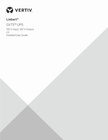
2015-10-17Port CPort ABlockdiagramATMEGA3232 general purposeprogrammable I/O lines(four 8-bit ports)Port BPort DErasmus 2015/2016, WIEiK, PKInput/OutputPeripheral Features 32 general purpose Programmable I/O Lines (4ports) Two 8-bit Timer/Counters with Separate Prescalersand Compare Modes One 16-bit Timer/Counter with Separate Prescaler,Compare Mode, and Capture Mode Real Time Counter with Separate Oscillator Four PWM Channels 8-channel, 10-bit ADC 8 Single-ended Channels– 7 Differential Channels in TQFP Package Only– 2 Differential Channels with Programmable Gain at 1x, 10x, or200x Byte-oriented Two-wire Serial InterfaceProgrammable Serial USARTMaster/Slave SPI Serial InterfaceProgrammable Watchdog Timer with Separate Onchip Oscillator On-chip Analog ComparatorErasmus 2015/2016, WIEiK, PK3
2015-10-17Port Operation RegistersThe following registers are related to the various portoperations that we can perform with the GPIO (GeneralPurpose Input Outout) pins.– DDRx – Data Direction Register– PORTx – Pin Output Register– PINx – Pin Input Registerwhere x GPIO port name (A, B, C or D)Data Direction RegisterPin Output RegisterPin Input RegisterErasmus 2015/2016, WIEiK, PKConfiguration ports and pins (lines) Each port pin consists of three register bits: DDxn, PORTxn, and PINxn.The DDxn bit in the DDRx Register selects the direction of this pin.– If DDxn is written logic one, Pxn is configured as an output pin.– If DDxn is written logic zero, Pxn is configured as an input pin.– If PORTxn is written logic one when the pin is configured as an input pin, the pull-up resistor isactivated.– To switch the pull-up resistor off, PORTxn has to be written logic zero or the pin has to beconfigured as an output pin. The port pins are tri-stated when a reset condition becomes active, even if noclocks are running.If PORTxn is written logic one when the pin is configured as an output pin, the portpin is driven high (one).If PORTxn is written logic zero when the pin is configured as an output pin, theport pin is driven low (zero).Each line (pin) of port can be set up individually (independent).Erasmus 2015/2016, WIEiK, PK4
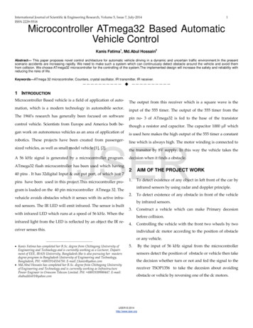
2015-10-17Ports features: All AVR ports have true Read-Modify-Writefunctionality when used as general digital I/Oports. This means that the direction of one port pin canbe changed without unintentionally changing thedirection of any other pin. The same applies when changing drive value (ifconfigured as output) or enabling/disabling ofpull-up resistors (if configured as input). Each output buffer has symmetrical drivecharacteristics with both high sink and sourcecapability. The pin driver is strong enough to drive LEDdisplays directly. All port pins have individually selectable pull-upresistors with a supply-voltage invariantresistance. All I/O pins have protection diodes to both VCCand Ground Most port pins are multiplexed with alternatefunctions for the peripheral features on thedevice.Erasmus 2015/2016, WIEiK, PKPorts in40-pin PDIP PackagesBasic NT1PD4/OC1BPD5/OC1APD6/ICPPD7/OC2 242526272829PC0PC1PC2PC3PC4PC5PC6PC7R4Vcc100C5 VCCC6AVCC10 Analog inputs on port A22pF12Y116MHz13C122pFC8100uF/10VPB6 1PB7 3/RESET 5C90.1uFJ10MISO VccSCK MOSIRES GND246PB5ISPVcc external crystal, external RESET button, additional components for AD converterErasmus 2015/2016, WIEiK, PK5
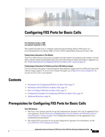
2015-10-17Driving Loads – source or sink configurations Vcc Vccsource currentMCUMCURoor ZoRoor ZoLoadLoadsink currentGND SOURCESINKGNDGNDGNDAn output pin not connected to anything is not of much interest. To do somethinguseful it must be connected to another device, referred here simply as a “load”.A real world load could be an LED, a lamp, a transistor, or some other circuitelement.Generally there are two ways to connect an output pin to a load.– The first is where the microcontroller supplies the current to drive the device. Themicrocontroller is referred to as the source. Current flows from the microcontroller power tothe output pin, through the load and to ground.– A microcontroller I/O pin can be set by the program to operate as an output. The outputvoltage will be close to the supply voltage when the output is set to a logical 1. The outputvoltage will be close to 0 volts when the pin is set to a logical 0.– The microcontroller pin can also “sink” the current as shown in Figure. Here the current flowsfrom the power supply through the load and through the output pin to ground. It is importantthat the load be connected to the same power supply line as the microcontroller, or you canErasmus 2015/2016, WIEiK, PKdestroy the IC.Digital Output Microcontrollers are somewhat delicate devices and the I/O lines can onlycarry a relatively small amount of current ( /-25mA). The current limit willdepend on the type of microcontroller, and the specific pin. There willusually be a maximum total current the pins of a single 8 bit port canhandle, as well as a limit for all of the outputs for the entiremicrocontroller. Exceeding the limits will destroy the microcontroller.To find out what the maximum currents are, you need to look at the datasheet for the microcontroller. PDF formatted data sheets can bedownloaded from the manufacturer. These can be quite large, severalhundred pages for a fairly complex one. Look for a section titled“Electrical Specifications” or something similar. Usually in the sectionthere will be a table called “Absolute Maximum Ratings” or similar. You willfind a table containing a number of specifications - Output Source Current(Ioh) and Output Sink Current (Iol)An output pin can either source or sink the current to or from a load. It isimportant not to exceed the maximum current ratings, which can be foundin the microcontroller’s data sheet.Erasmus 2015/2016, WIEiK, PK6
2015-10-17Digital input Vcc Vcc1 Vcc2 Vcc1 Vcc2 Vcc1DigitalCircuitDigitalCircuitMCUMCUVinVinGND Vcc2GNDGND A pin with a low input voltage (ideally 0 volts) will read as a logical 0. A pin with a input voltage near Vcc (or Vdd) will read as a logic 1. As a first approximation, any input less than half of Vcc will read as a 0, and anyinput over Vcc/2 will read as a 1. There is a voltage band however, right around Vcc/2, where there is noguarantee what state will be read. Figure shows the logic thresholds of atypical microcontroller. The X axis represents the supply voltage, Vcc (Vdd on some data sheets). TheY axis represents the voltage on an input pin. The black dashed line is wherethe input is 1/2 Vcc. For a given supply voltage if the input pin voltage is below the green line thepin will be read as 0. Above the blue line the input will read as 1. Between the green and blue lines is a “no man’s land” where it might read as a0 or it might read as a 1. If the signal is near Vcc/2, a little noise can cause thevoltage to jump over to the other side, and cause an incorrect reading.Erasmus 2015/2016, WIEiK, PKDigital input – pull up or pull down resistorInternal or external pull up resistor VccInternal or external pull down resistor VccRpuMCUSwitchMCUSwitchVinRpdVinGND GNDSometimes you want an input to read as a 1 or 0 as a default. Suppose you have a sensor on a cable that plugsinto your device. It is possible that the user will disconnect the cable. If the input pin is left floating, it mightsometimes read as a 1, sometimes as a 0. Your code might interpret this as changes from a sensor and not act theway you want.Putting a pull up resistor will set the input voltage near Vcc and it will read as a 1. A pull down resistor will bringthe voltage near 0V, and it will read as a zero. Figure shows pull up and pull down resistors. The switch, sensor, orother component that generates the normal 1 and 0 voltages must be able to over drive the resistor.Some microcontrollers have internal pull ups. You set a bit in an internal register to turn them on. These are nicebecause you don’t have to add the pull up resistors in the hardware design, saving cost, board space and assemblytime. The value of internal pull ups is usually pretty high (weak pull up), and the actual value often has a hugerange. Internal pull ups are handy, but evaluate the parameters in the data sheet before using them.So, what values should be used for pull ups and pull downs? There are no hard and fast rules, but generallyanything under a few thousand ohms is a strong pull up. Weak pull ups often reach 40-50KΩ.Erasmus 2015/2016, WIEiK, PK7
2015-10-17Digital input The DDR register in the ATmega32 will control if a pin is aninput or output. You need your program to set up the portdirection registers as an early step when power is applied tothe chip or it comes out of reset. I/O pins are usually configured in groups of 8 bit I/Oports. The program can read the port and will get a valuebetween 0 and 255 depending on the states of the inputpins. In assembly language programming there will usually be opcode instructions that allow reading a single pin of a port. C compilers will usually implement single bit functions aswell. Otherwise the programmer will have to read the entireport and mask off the other bits.Erasmus 2015/2016, WIEiK, PK8
Input/Ouput ports in ATmega32 The ATmega32 has four 8-bit I/O ports named PORTA, PORTB, PORTC and PORTD, which are all general purpose and most have dual functions. The PORTA can be used for reading analogue quantities via the A/D converter. When we are going to use input/output ports, we have to set