Transcription
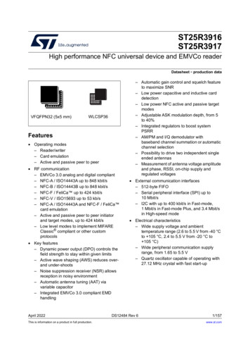
ST25R3916ST25R3917High performance NFC universal device and EMVCo readerDatasheet - production dataVFQFPN32 (5x5 mm)WLCSP36Features Operating modes– Reader/writer– Card emulation– Active and passive peer to peer RF communication– EMVCo 3.0 analog and digital compliant– NFC-A / ISO14443A up to 848 kbit/s– NFC-B / ISO14443B up to 848 kbit/s– NFC-F / FeliCa up to 424 kbit/s– NFC-V / ISO15693 up to 53 kb/s– NFC-A / ISO14443A and NFC-F / FeliCa card emulation– Active and passive peer to peer initiatorand target modes, up to 424 kbit/s– Low level modes to implement MIFAREClassic compliant or other customprotocols Key features– Dynamic power output (DPO) controls thefield strength to stay within given limits– Active wave shaping (AWS) reduces overand under-shoots– Noise suppression receiver (NSR) allowsreception in noisy environment– Automatic antenna tuning (AAT) viavariable capacitor– Integrated EMVCo 3.0 compliant EMDhandlingApril 2022This is information on a product in full production.– Automatic gain control and squelch featureto maximize SNR– Low power capacitive and inductive carddetection– Low power NFC active and passive targetmodes– Adjustable ASK modulation depth, from 5to 40%– Integrated regulators to boost systemPSRR– AM/PM and I/Q demodulator withbaseband channel summation or automaticchannel selection– Possibility to drive two independent singleended antennas– Measurement of antenna voltage amplitudeand phase, RSSI, on-chip supply andregulated voltages External communication interfaces– 512-byte FIFO– Serial peripheral interface (SPI) up to10 Mbit/s– I2C with up to 400 kbit/s in Fast-mode,1 Mbit/s in Fast-mode Plus, and 3.4 Mbit/sin High-speed mode Electrical characteristics– Wide supply voltage and ambienttemperature range (2.6 to 5.5 V from -40 Cto 105 C, 2.4 to 5.5 V from -20 C to 105 C)– Wide peripheral communication supplyrange, from 1.65 to 5.5 V– Quartz oscillator capable of operating with27.12 MHz crystal with fast start-upDS12484 Rev 61/157www.st.com
ContentsST25R3916/7Contents1Applications . . . . . . . . . . . . . . . . . . . . . . . . . . . . . . . . . . . . . . . . . . . . . . . 112Description . . . . . . . . . . . . . . . . . . . . . . . . . . . . . . . . . . . . . . . . . . . . . . . . 122.1System diagram . . . . . . . . . . . . . . . . . . . . . . . . . . . . . . . . . . . . . . . . . . . . 132.2Block diagram . . . . . . . . . . . . . . . . . . . . . . . . . . . . . . . . . . . . . . . . . . . . . . 152.2.1Transmitter . . . . . . . . . . . . . . . . . . . . . . . . . . . . . . . . . . . . . . . . . . . . . . . 152.2.2Receiver . . . . . . . . . . . . . . . . . . . . . . . . . . . . . . . . . . . . . . . . . . . . . . . . . 162.2.3Phase and amplitude detector . . . . . . . . . . . . . . . . . . . . . . . . . . . . . . . . 162.2.4Automatic antenna tuning (AAT) . . . . . . . . . . . . . . . . . . . . . . . . . . . . . . 162.2.5A/D converter . . . . . . . . . . . . . . . . . . . . . . . . . . . . . . . . . . . . . . . . . . . . . 162.2.6Capacitive sensor . . . . . . . . . . . . . . . . . . . . . . . . . . . . . . . . . . . . . . . . . 162.2.7External field detector . . . . . . . . . . . . . . . . . . . . . . . . . . . . . . . . . . . . . . 172.2.8Quartz crystal oscillator . . . . . . . . . . . . . . . . . . . . . . . . . . . . . . . . . . . . . 172.2.9Power supply regulators . . . . . . . . . . . . . . . . . . . . . . . . . . . . . . . . . . . . 172.2.10POR and bias . . . . . . . . . . . . . . . . . . . . . . . . . . . . . . . . . . . . . . . . . . . . 172.2.11RC oscillator and Wake-up timer . . . . . . . . . . . . . . . . . . . . . . . . . . . . . . 172.2.12TX encoding . . . . . . . . . . . . . . . . . . . . . . . . . . . . . . . . . . . . . . . . . . . . . . 182.2.13RX decoding . . . . . . . . . . . . . . . . . . . . . . . . . . . . . . . . . . . . . . . . . . . . . 182.2.14FIFO . . . . . . . . . . . . . . . . . . . . . . . . . . . . . . . . . . . . . . . . . . . . . . . . . . . . 182.2.15Control logic . . . . . . . . . . . . . . . . . . . . . . . . . . . . . . . . . . . . . . . . . . . . . . 182.2.16Host interface . . . . . . . . . . . . . . . . . . . . . . . . . . . . . . . . . . . . . . . . . . . . . 182.2.17Passive target memory . . . . . . . . . . . . . . . . . . . . . . . . . . . . . . . . . . . . . 182.2.18P2RAM . . . . . . . . . . . . . . . . . . . . . . . . . . . . . . . . . . . . . . . . . . . . . . . . . 183Pin and signal description . . . . . . . . . . . . . . . . . . . . . . . . . . . . . . . . . . . 194Application information . . . . . . . . . . . . . . . . . . . . . . . . . . . . . . . . . . . . . 232/1574.1Power-on sequence . . . . . . . . . . . . . . . . . . . . . . . . . . . . . . . . . . . . . . . . . 234.2Operating modes . . . . . . . . . . . . . . . . . . . . . . . . . . . . . . . . . . . . . . . . . . . 234.2.1Transmitter . . . . . . . . . . . . . . . . . . . . . . . . . . . . . . . . . . . . . . . . . . . . . . . 234.2.2Receiver . . . . . . . . . . . . . . . . . . . . . . . . . . . . . . . . . . . . . . . . . . . . . . . . . 264.2.3Antenna tuning . . . . . . . . . . . . . . . . . . . . . . . . . . . . . . . . . . . . . . . . . . . . 314.2.4Capacitive sensor . . . . . . . . . . . . . . . . . . . . . . . . . . . . . . . . . . . . . . . . . 314.2.5Wake-up mode . . . . . . . . . . . . . . . . . . . . . . . . . . . . . . . . . . . . . . . . . . . . 33DS12484 Rev 6
ST25R3916/74.34.44.5Contents4.2.6Quartz crystal oscillator . . . . . . . . . . . . . . . . . . . . . . . . . . . . . . . . . . . . . 344.2.7Timers . . . . . . . . . . . . . . . . . . . . . . . . . . . . . . . . . . . . . . . . . . . . . . . . . . 344.2.8A/D converter . . . . . . . . . . . . . . . . . . . . . . . . . . . . . . . . . . . . . . . . . . . . . 374.2.9Phase and amplitude detector . . . . . . . . . . . . . . . . . . . . . . . . . . . . . . . . 374.2.10External field detector . . . . . . . . . . . . . . . . . . . . . . . . . . . . . . . . . . . . . . 384.2.11Power supply system . . . . . . . . . . . . . . . . . . . . . . . . . . . . . . . . . . . . . . . 394.2.12Overshoot / undershoot protection . . . . . . . . . . . . . . . . . . . . . . . . . . . . 424.2.13Reader operation . . . . . . . . . . . . . . . . . . . . . . . . . . . . . . . . . . . . . . . . . . 424.2.14Listen mode . . . . . . . . . . . . . . . . . . . . . . . . . . . . . . . . . . . . . . . . . . . . . . 43Communication with an external microcontroller . . . . . . . . . . . . . . . . . . . 474.3.1Interrupt interface . . . . . . . . . . . . . . . . . . . . . . . . . . . . . . . . . . . . . . . . . . 474.3.2Communication interface selection . . . . . . . . . . . . . . . . . . . . . . . . . . . . 484.3.3Serial peripheral interface (SPI) . . . . . . . . . . . . . . . . . . . . . . . . . . . . . . . 484.3.4I2C interface . . . . . . . . . . . . . . . . . . . . . . . . . . . . . . . . . . . . . . . . . . . . . 54Direct commands . . . . . . . . . . . . . . . . . . . . . . . . . . . . . . . . . . . . . . . . . . . 594.4.1Set default . . . . . . . . . . . . . . . . . . . . . . . . . . . . . . . . . . . . . . . . . . . . . . . 604.4.2Stop all activities . . . . . . . . . . . . . . . . . . . . . . . . . . . . . . . . . . . . . . . . . . 614.4.3Clear FIFO . . . . . . . . . . . . . . . . . . . . . . . . . . . . . . . . . . . . . . . . . . . . . . . 614.4.4Transmit commands . . . . . . . . . . . . . . . . . . . . . . . . . . . . . . . . . . . . . . . 614.4.5NFC field ON commands . . . . . . . . . . . . . . . . . . . . . . . . . . . . . . . . . . . . 624.4.6Mask receive data and Unmask receive data . . . . . . . . . . . . . . . . . . . . 634.4.7Change AM modulation state . . . . . . . . . . . . . . . . . . . . . . . . . . . . . . . . . 644.4.8Measure amplitude . . . . . . . . . . . . . . . . . . . . . . . . . . . . . . . . . . . . . . . . 644.4.9Reset RX gain . . . . . . . . . . . . . . . . . . . . . . . . . . . . . . . . . . . . . . . . . . . . 644.4.10Adjust regulators . . . . . . . . . . . . . . . . . . . . . . . . . . . . . . . . . . . . . . . . . . 644.4.11Measure phase . . . . . . . . . . . . . . . . . . . . . . . . . . . . . . . . . . . . . . . . . . . 644.4.12Clear RSSI . . . . . . . . . . . . . . . . . . . . . . . . . . . . . . . . . . . . . . . . . . . . . . . 654.4.13Transparent mode . . . . . . . . . . . . . . . . . . . . . . . . . . . . . . . . . . . . . . . . . 654.4.14Calibrate capacitive sensor . . . . . . . . . . . . . . . . . . . . . . . . . . . . . . . . . . 654.4.15Measure capacitance . . . . . . . . . . . . . . . . . . . . . . . . . . . . . . . . . . . . . . . 654.4.16Measure power supply . . . . . . . . . . . . . . . . . . . . . . . . . . . . . . . . . . . . . . 664.4.17Test access . . . . . . . . . . . . . . . . . . . . . . . . . . . . . . . . . . . . . . . . . . . . . . 66Registers . . . . . . . . . . . . . . . . . . . . . . . . . . . . . . . . . . . . . . . . . . . . . . . . . 684.5.1IO configuration register 1 . . . . . . . . . . . . . . . . . . . . . . . . . . . . . . . . . . . 714.5.2IO configuration register 2 . . . . . . . . . . . . . . . . . . . . . . . . . . . . . . . . . . . 724.5.3Operation control register . . . . . . . . . . . . . . . . . . . . . . . . . . . . . . . . . . . 734.5.4Mode definition register . . . . . . . . . . . . . . . . . . . . . . . . . . . . . . . . . . . . . 74DS12484 Rev 63/1576
Contents4/157ST25R3916/74.5.5Bit rate definition register . . . . . . . . . . . . . . . . . . . . . . . . . . . . . . . . . . . . 754.5.6ISO14443A and NFC 106kb/s settings register . . . . . . . . . . . . . . . . . . . 764.5.7ISO14443B settings register 1 . . . . . . . . . . . . . . . . . . . . . . . . . . . . . . . . 774.5.8ISO14443B and FeliCa settings register . . . . . . . . . . . . . . . . . . . . . . . . 784.5.9NFCIP-1 passive target definition register . . . . . . . . . . . . . . . . . . . . . . . 794.5.10Stream mode definition register . . . . . . . . . . . . . . . . . . . . . . . . . . . . . . . 804.5.11Auxiliary definition register . . . . . . . . . . . . . . . . . . . . . . . . . . . . . . . . . . . 814.5.12EMD suppression configuration register . . . . . . . . . . . . . . . . . . . . . . . . 824.5.13Subcarrier start timer register . . . . . . . . . . . . . . . . . . . . . . . . . . . . . . . . 834.5.14Receiver configuration register 1 . . . . . . . . . . . . . . . . . . . . . . . . . . . . . . 844.5.15Receiver configuration register 2 . . . . . . . . . . . . . . . . . . . . . . . . . . . . . . 854.5.16Receiver configuration register 3 . . . . . . . . . . . . . . . . . . . . . . . . . . . . . . 864.5.17Receiver configuration register 4 . . . . . . . . . . . . . . . . . . . . . . . . . . . . . . 864.5.18P2P receiver configuration register 1 . . . . . . . . . . . . . . . . . . . . . . . . . . . 874.5.19Correlator configuration register 1 . . . . . . . . . . . . . . . . . . . . . . . . . . . . . 884.5.20Correlator configuration register 2 . . . . . . . . . . . . . . . . . . . . . . . . . . . . . 894.5.21Mask receive timer register . . . . . . . . . . . . . . . . . . . . . . . . . . . . . . . . . . 904.5.22No-response timer register 1 . . . . . . . . . . . . . . . . . . . . . . . . . . . . . . . . . 914.5.23No-response timer register 2 . . . . . . . . . . . . . . . . . . . . . . . . . . . . . . . . . 914.5.24Timer and EMV control register . . . . . . . . . . . . . . . . . . . . . . . . . . . . . . 924.5.25General purpose timer register 1 . . . . . . . . . . . . . . . . . . . . . . . . . . . . . . 934.5.26General purpose timer register 2 . . . . . . . . . . . . . . . . . . . . . . . . . . . . . . 934.5.27PPON2 field waiting register . . . . . . . . . . . . . . . . . . . . . . . . . . . . . . . . . 944.5.28Squelch timer register . . . . . . . . . . . . . . . . . . . . . . . . . . . . . . . . . . . . . . 954.5.29NFC field on guard timer register . . . . . . . . . . . . . . . . . . . . . . . . . . . . . . 954.5.30Mask main interrupt register . . . . . . . . . . . . . . . . . . . . . . . . . . . . . . . . . 964.5.31Mask timer and NFC interrupt register . . . . . . . . . . . . . . . . . . . . . . . . . . 964.5.32Mask error and wake-up interrupt register . . . . . . . . . . . . . . . . . . . . . . . 974.5.33Mask passive target interrupt register . . . . . . . . . . . . . . . . . . . . . . . . . . 974.5.34Main interrupt register . . . . . . . . . . . . . . . . . . . . . . . . . . . . . . . . . . . . . . 984.5.35Timer and NFC interrupt register . . . . . . . . . . . . . . . . . . . . . . . . . . . . . . 994.5.36Error and wake-up interrupt register . . . . . . . . . . . . . . . . . . . . . . . . . . 1004.5.37Passive target interrupt register . . . . . . . . . . . . . . . . . . . . . . . . . . . . . . 1014.5.38FIFO status register 1 . . . . . . . . . . . . . . . . . . . . . . . . . . . . . . . . . . . . . 1024.5.39FIFO status register 2 . . . . . . . . . . . . . . . . . . . . . . . . . . . . . . . . . . . . . 1024.5.40Collision display register . . . . . . . . . . . . . . . . . . . . . . . . . . . . . . . . . . . 1034.5.41Passive target display register . . . . . . . . . . . . . . . . . . . . . . . . . . . . . . . 104DS12484 Rev 6
ST25R3916/7Contents4.5.42Number of transmitted bytes register 1 . . . . . . . . . . . . . . . . . . . . . . . . 1054.5.43Number of transmitted bytes register 2 . . . . . . . . . . . . . . . . . . . . . . . . 1054.5.44Bit rate detection display register . . . . . . . . . . . . . . . . . . . . . . . . . . . . . 1064.5.45A/D converter output register . . . . . . . . . . . . . . . . . . . . . . . . . . . . . . . . 1074.5.46Antenna tuning control register 1 . . . . . . . . . . . . . . . . . . . . . . . . . . . . . 1084.5.47Antenna tuning control register 2 . . . . . . . . . . . . . . . . . . . . . . . . . . . . . 1084.5.48TX driver register . . . . . . . . . . . . . . . . . . . . . . . . . . . . . . . . . . . . . . . . . 1094.5.49Auxiliary modulation setting register . . . . . . . . . . . . . . . . . . . . . . . . . . 1114.5.50Passive target modulation register . . . . . . . . . . . . . . . . . . . . . . . . . . . 1124.5.51TX driver timing register . . . . . . . . . . . . . . . . . . . . . . . . . . . . . . . . . . . . 1134.5.52External field detector activation threshold register . . . . . . . . . . . . . . . 1144.5.53Resistive AM modulation register . . . . . . . . . . . . . . . . . . . . . . . . . . . . 1154.5.54External field detector deactivation threshold register . . . . . . . . . . . . . 1174.5.55TX driver timing display register . . . . . . . . . . . . . . . . . . . . . . . . . . . . . 1194.5.56Regulator voltage control register . . . . . . . . . . . . . . . . . . . . . . . . . . . . 1204.5.57Regulator display register . . . . . . . . . . . . . . . . . . . . . . . . . . . . . . . . . . 1214.5.58RSSI display register . . . . . . . . . . . . . . . . . . . . . . . . . . . . . . . . . . . . . . 1224.5.59Gain reduction state register . . . . . . . . . . . . . . . . . . . . . . . . . . . . . . . . 1234.5.60Capacitive sensor control register . . . . . . . . . . . . . . . . . . . . . . . . . . . . 1244.5.61Capacitive sensor display register . . . . . . . . . . . . . . . . . . . . . . . . . . . . 1244.5.62Auxiliary display register . . . . . . . . . . . . . . . . . . . . . . . . . . . . . . . . . . . 1254.5.63Overshoot protection configuration register 1 . . . . . . . . . . . . . . . . . . . 1264.5.64Overshoot protection configuration register 2 . . . . . . . . . . . . . . . . . . . 1264.5.65Undershoot protection configuration register 1 . . . . . . . . . . . . . . . . . . 1274.5.66Undershoot protection configuration register 2 . . . . . . . . . . . . . . . . . . 1274.5.67Wake-up timer control register . . . . . . . . . . . . . . . . . . . . . . . . . . . . . . . 1284.5.68Amplitude measurement configuration register . . . . . . . . . . . . . . . . . . 1294.5.69Amplitude measurement reference register . . . . . . . . . . . . . . . . . . . . . 1294.5.70Amplitude measurement auto-averaging display register . . . . . . . . . . 1304.5.71Amplitude measurement display register . . . . . . . . . . . . . . . . . . . . . . . 1304.5.72Phase measurement configuration register . . . . . . . . . . . . . . . . . . . . . 1314.5.73Phase measurement reference register . . . . . . . . . . . . . . . . . . . . . . . 1314.5.74Phase measurement auto-averaging display register . . . . . . . . . . . . . 1324.5.75Phase measurement display register . . . . . . . . . . . . . . . . . . . . . . . . . 1324.5.76Capacitance measurement configuration register . . . . . . . . . . . . . . . . 1334.5.77Capacitance measurement reference register . . . . . . . . . . . . . . . . . . . 1334.5.78Capacitance measurement auto-averaging display register . . . . . . . . 134DS12484 Rev 65/1576
Contents56ST25R3916/74.5.79Capacitance measurement display register . . . . . . . . . . . . . . . . . . . . . 1344.5.80IC identity register . . . . . . . . . . . . . . . . . . . . . . . . . . . . . . . . . . . . . . . . 135Electrical characteristics . . . . . . . . . . . . . . . . . . . . . . . . . . . . . . . . . . . 1365.1Absolute maximum ratings . . . . . . . . . . . . . . . . . . . . . . . . . . . . . . . . . . . 1365.2Operating conditions . . . . . . . . . . . . . . . . . . . . . . . . . . . . . . . . . . . . . . . 1375.3DC/AC characteristics for digital inputs and outputs . . . . . . . . . . . . . . . 1385.4Electrical characteristics . . . . . . . . . . . . . . . . . . . . . . . . . . . . . . . . . . . . . 1395.5SPI interface characteristics . . . . . . . . . . . . . . . . . . . . . . . . . . . . . . . . . . 1435.6I2C interface characteristics . . . . . . . . . . . . . . . . . . . . . . . . . . . . . . . . . . 145Package information . . . . . . . . . . . . . . . . . . . . . . . . . . . . . . . . . . . . . . . 1506.1VFQFPN32 package information . . . . . . . . . . . . . . . . . . . . . . . . . . . . . . 1506.2WLCSP36 package information . . . . . . . . . . . . . . . . . . . . . . . . . . . . . . . 1527Ordering information . . . . . . . . . . . . . . . . . . . . . . . . . . . . . . . . . . . . . . 1548Revision history . . . . . . . . . . . . . . . . . . . . . . . . . . . . . . . . . . . . . . . . . . 1556/157DS12484 Rev 6
ST25R3916/7List of tablesList of tablesTable 1.Table 2.Table 3.Table 4.Table 5.Table 6.Table 7.Table 8.Table 9.Table 10.Table 11.Table 12.Table 13.Table 14.Table 15.Table 16.Table 17.Table 18.Table 19.Table 20.Table 21.Table 22.Table 23.Table 24.Table 25.Table 26.Table 27.Table 28.Table 29.Table 30.Table 31.Table 32.Table 33.Table 34.Table 35.Table 36.Table 37.Table 38.Table 39.Table 40.Table 41.Table 42.Table 43.Table 44.Table 45.Table 46.Table 47.Table 48.List of features . . . . . . . . . . . . . . . . . . . . . . . . . . . . . . . . . . . . . . . . . . . . . . . . . . . . . . . . . . 11ST25R3916 - VFQFPN32 and WLCSP36 pin assignment . . . . . . . . . . . . . . . . . . . . . . . . . 20ST25R3917 - VFQFPN32 pin assignment . . . . . . . . . . . . . . . . . . . . . . . . . . . . . . . . . . . . . 21RX channel selection . . . . . . . . . . . . . . . . . . . . . . . . . . . . . . . . . . . . . . . . . . . . . . . . . . . . . 26Low-pass control. . . . . . . . . . . . . . . . . . . . . . . . . . . . . . . . . . . . . . . . . . . . . . . . . . . . . . . . . 28First and third zero setting . . . . . . . . . . . . . . . . . . . . . . . . . . . . . . . . . . . . . . . . . . . . . . . . . 28PT Memory address space . . . . . . . . . . . . . . . . . . . . . . . . . . . . . . . . . . . . . . . . . . . . . . . . 45NFC-212/424k SENS RES format . . . . . . . . . . . . . . . . . . . . . . . . . . . . . . . . . . . . . . . . . . . 46IRQ output . . . . . . . . . . . . . . . . . . . . . . . . . . . . . . . . . . . . . . . . . . . . . . . . . . . . . . . . . . . . . 47Serial data interface (4-wire interface) signal lines . . . . . . . . . . . . . . . . . . . . . . . . . . . . . . . 49SPI operation modes . . . . . . . . . . . . . . . . . . . . . . . . . . . . . . . . . . . . . . . . . . . . . . . . . . . . . 50I2C interface and interrupt signal lines . . . . . . . . . . . . . . . . . . . . . . . . . . . . . . . . . . . . . . . . 55List of direct commands . . . . . . . . . . . . . . . . . . . . . . . . . . . . . . . . . . . . . . . . . . . . . . . . . . . 59Timing parameters of NFC field ON commands . . . . . . . . . . . . . . . . . . . . . . . . . . . . . . . . . 63Analog test and observation register 1 . . . . . . . . . . . . . . . . . . . . . . . . . . . . . . . . . . . . . . . . 66Test access register - Signal selection of CSI and CSO pins . . . . . . . . . . . . . . . . . . . . . . . 67List of registers - Space A. . . . . . . . . . . . . . . . . . . . . . . . . . . . . . . . . . . . . . . . . . . . . . . . . . 68List of registers - Space B. . . . . . . . . . . . . . . . . . . . . . . . . . . . . . . . . . . . . . . . . . . . . . . . . . 70IO configuration register 1 . . . . . . . . . . . . . . . . . . . . . . . . . . . . . . . . . . . . . . . . . . . . . . . . . 71IO configuration register 2 . . . . . . . . . . . . . . . . . . . . . . . . . . . . . . . . . . . . . . . . . . . . . . . . . 72Operation control register . . . . . . . . . . . . . . . . . . . . . . . . . . . . . . . . . . . . . . . . . . . . . . . . . . 73Mode definition register . . . . . . . . . . . . . . . . . . . . . . . . . . . . . . . . . . . . . . . . . . . . . . . . . . . 74Initiator operation modes . . . . . . . . . . . . . . . . . . . . . . . . . . . . . . . . . . . . . . . . . . . . . . . . . . 74Target operation modes . . . . . . . . . . . . . . . . . . . . . . . . . . . . . . . . . . . . . . . . . . . . . . . . . . . 74Bit rate definition register . . . . . . . . . . . . . . . . . . . . . . . . . . . . . . . . . . . . . . . . . . . . . . . . . . 75Bit rate coding . . . . . . . . . . . . . . . . . . . . . . . . . . . . . . . . . . . . . . . . . . . . . . . . . . . . . . . . . . . 75ISO14443A and NFC 106kb/s settings register . . . . . . . . . . . . . . . . . . . . . . . . . . . . . . . . . 76ISO14443A modulation pulse width . . . . . . . . . . . . . . . . . . . . . . . . . . . . . . . . . . . . . . . . . . 76ISO14443B settings register 1 . . . . . . . . . . . . . . . . . . . . . . . . . . . . . . . . . . . . . . . . . . . . . . 77ISO14443B and FeliCa settings register . . . . . . . . . . . . . . . . . . . . . . . . . . . . . . . . . . . . . . 78Minimum TR1 codings . . . . . . . . . . . . . . . . . . . . . . . . . . . . . . . . . . . . . . . . . . . . . . . . . . . . 78NFCIP-1 passive target definition register . . . . . . . . . . . . . . . . . . . . . . . . . . . . . . . . . . . . . 79Stream mode definition register . . . . . . . . . . . . . . . . . . . . . . . . . . . . . . . . . . . . . . . . . . . . . 80Sub-carrier frequency definition for Sub-carrier stream mode . . . . . . . . . . . . . . . . . . . . . . 80Definition of time period for Stream mode Tx modulator control. . . . . . . . . . . . . . . . . . . . . 80Auxiliary definition register . . . . . . . . . . . . . . . . . . . . . . . . . . . . . . . . . . . . . . . . . . . . . . . . . 81RW receiver operation . . . . . . . . . . . . . . . . . . . . . . . . . . . . . . . . . . . . . . . . . . . . . . . . . . . . 81EMD suppression configuration register . . . . . . . . . . . . . . . . . . . . . . . . . . . . . . . . . . . . . . . 82Subcarrier start timer register . . . . . . . . . . . . . . . . . . . . . . . . . . . . . . . . . . . . . . . . . . . . . . . 83Receiver configuration register 1 . . . . . . . . . . . . . . . . . . . . . . . . . . . . . . . . . . . . . . . . . . . . 84Receiver configuration register 2 . . . . . . . . . . . . . . . . . . . . . . . . . . . . . . . . . . . . . . . . . . . . 85Receiver configuration register 3 . . . . . . . . . . . . . . . . . . . . . . . . . . . . . . . . . . . . . . . . . . . . 86Receiver configuration register 4 . . . . . . . . . . . . . . . . . . . . . . . . . . . . . . . . . . . . . . . . . . . . 86P2P receiver configuration register 1 . . . . . . . . . . . . . . . . . . . . . . . . . . . . . . . . . . . . . . . . . 87OOK threshold level settings . . . . . . . . . . . . . . . . . . . . . . . . . . . . . . . . . . . . . . . . . . . . . . . 87Correlator configuration register 1 . . . . . . . . . . . . . . . . . . . . . . . . . . . . . . . . . . . . . . . . . . . 88Correlator configuration register 2 . . . . . . . . . . . . . . . . . . . . . . . . . . . . . . . . . . . . . . . . . . . 89Mask receive timer register. . . . . . . . . . . . . . . . . . . . . . . . . . . . . . . . . . . . . . . . . . . . . . . . . 90DS12484 Rev 67/1579
List of tablesTable 49.Table 50.Table 51.Table 52.Table 53.Table 54.Table 55.Table 56.Table 57.Table 58.Table 59.Table 60.Table 61.Table 62.Table 63.Table 64.Table 65.Table 66.Table 67.Table 68.Table 69.Table 70.Table 71.Table 72.Table 73.Table 74.Table 75.Table 76.Table 77.Table 78.Table 79.Table 80.Table 81.Table 82.Table 83.Table 84.Table 85.Table 86.Table 87.Table 88.Table 89.Table 90.Table 91.Table 92.Table 93.Table 94.Table 95.Table 96.Table 97.Table 98.Table 99.Table 100.8/157ST25R3916/7No-response timer register 1 . . . . . . . . . . . . . . . . . . . . . . . . . . . . . . . . . . . . . . . . . . . . . . . 91No-response timer register 2 . . . . . . . . . . . . . . . . . . . . . . . . . . . . . . . . . . . . . . . . . . . . . . . 91Timer and EMV control register . . . . . . . . . . . . . . . . . . . . . . . . . . . . . . . . . . . . . . . . . . . . . 92Trigger sources . . . . . . . . . . . . . . . . . . . . . . . . . . . . . . . . . . . . . . . . . . . . . . . . . . . . . . . . . . 92General purpose timer register 1 . . . . . . . . . . . . . . . . . . . . . . . . . . . . . . . . . . . . . . . . . . . . 93General purpose timer register 2 . . . . . . . . . . . . . . . . . . . . . . . . . . . . . . . . . . . . . . . . . . . . 93PPON2 field waiting register . . . . . . . . . . . . . . . . . . . . . . . . . . . . . . . . . . . . . . . . . . . . . . . . 94Squelch timer register . . . . . . . . . . . . . . . . . . . . . . . . . . . . . . . . . . . . . . . . . . . . . . . . . . . . . 95NFC field on guard timer register . . . . . . . . . . . . . . . . . . . . . . . . . . . . . . . . . . . . . . . . . . . . 95Mask main interrupt register . . . . . . . . . . . . . . . . . . . . . . . . . . . . . . . . . . . . . . . . . . . . . . . . 96Mask timer and NFC interrupt register . . . . . . . . . . . . . . . . . . . . . . . . . . . . . . . . . . . . . . . . 96Mask error and wake-up interrupt register . . . . . . . . . . . . . . . . . . . . . . . . . . . . . . . . . . . . . 97Mask passive target interrupt register. . . . . . . . . . . . . . . . . . . . . . . . . . . . . . . . . . . . . . . . . 97Main interrupt register . . . . . . . . . . . . . . . . . . . . . . . . . . . . . . . . . . . . . . . . . . . . . . . . . . . . . 98Timer and NFC interrupt register . . . . . . . . . . . . . . . . . . . . . . . . . . . . . . . . . . . . . . . . . . . . 99Error and wake-up interrupt register . . . . . . . . . . . . . . . . . . . . . . . . . . . . . . . . . . . . . . . . . 100Passive target interrupt register . . . . . . . . . . . . . . . . . . . . . . . . . . . . . . . . . . . . . . . . . . . . 101FIFO status register 1 . . . . . . . . . . . . . . . . . . . . . . . . . . . . . . . . . . . . . . . . . . . . . . . . . . . . 102FIFO status register 2 . . . . . . . . . . . . . . . . . . . . . . . . . . . . . . . . . . . . . . . . . . . . . . . . . . . . 102Collision display register . . . . . . . . . . . . . . . . . . . . . . . . . . . . . . . . . . . . . . . . . . . . . . . . . . 103Passive target display register . . . . . . . . . . . . . . . . . . . . . . . . . . . . . . . . . . . . . . . . . . . . . 104Number of transmitted bytes register 1. . . . . . . . . . . . . . . . . . . . . . . . . . . . . . . . . . . . . . . 105Number of transmitted bytes register 2 . . . . . . . . . . . . . . . . . . . . . . . . . . . . . . . . . . . . . . 105Bit rate detection display register . . . . . . . . . . . . . . . . . . . . . . . . . . . . . . . . . . . . . . . . . . . 106A/D converter output register . . . . . . . . . . . . . . . . . . . . . . . . . . . . . . . . . . . . . . . . . . . . . . 107Antenna tuning control register 1 . . . . . . . . . . . . . . . . . . . . . . . . . . . . . . . . . . . . . . . . . . . 108Antenna tuning control register 2 . . . . . . . . . . . . . . . . . . . . . . . . . . . . . . . . . . . . . . . . . . . 108TX driver register . . . . . . . . . . . . . . . . . . . . . . . . . . . . . . . . . . . . . . . . . . . . . . . . . . . . . . . 109AM modulation index . . . . . . . . . . . . . . . . . . . . . . . . . . . . . . . . . . . . . . . . . . . . . . . . . . . . 109RFO driver resistance . . . . . . . . . . . . . . . . . . . . . . . . . . . . . . . . . . . . . . . . . . . . . . . . . . . . 110Auxiliary modulation setting register . . . . . . . . . . . . . . . . . . . . . . . . . . . . . . . . . . . . . . . . . 111Passive target modulation register . . . . . . . . . . . . . . . . . . . . . . . . . . . . . . . . . . . . . . . . . . 112Passive target modulated and unmodulated state driver output resistance . . . . . . . . . . . 112TX driver timing register . . . . . . . . . . . . . . . . . . . . . . . . . . . . . . . . . . . . . . . . . . . . . . . . . . 113External field detector activation threshold register . . . . . . . . . . . . . . . . . . . . . . . . . . . . . 114Resistive AM modulation register . . . . . . . . . . . . . . . . . . . . . . . . . . . . . . . . . . . . . . . . . . . 115Resistive AM modulated state driver output resistance . . . . . . . . . . . . . . . . . . . . . . . . . . 115External field detector deactivation threshold register . . . . . . . . . . . . . . . . . . . . . . . . . . . 117Peer detection threshold as seen on RFI1 input. . . . . . . . . . . . . . . . . . . . . . . . . . . . . . . . 118Collision avoidance thres
This is information on a product in full production. April 2022 DS12484 Rev 6 1/157 ST25R3916 ST25R3917 High performance NFC universal device and EMVCo reader