Transcription
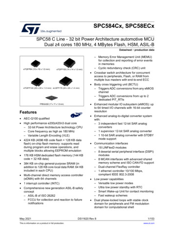
SPC584Cx, SPC58ECxSPC58 C Line - 32 bit Power Architecture automotive MCUDual z4 cores 180 MHz, 4 MBytes Flash, HSM, ASIL-BDatasheet - production dataeTQFP64 (10 x 10 x 1.0 mm)eTQFP100 (14 x 14 x 1.0 mm)– Memory Error Management Unit (MEMU)for collection and reporting of error eventsin memories– Cyclic redundancy check (CRC) unit Crossbar switch architecture for concurrentaccess to peripherals, Flash, or RAM frommultiple bus masters with end-to-end ECCeTQFP144 (20 x 20 x 1.0 mm) eLQFP176 (24 x 24 x 1.4 mm) Enhanced modular IO subsystem (eMIOS): upto 64 timed I/O channels with 16-bit counterresolutionFPBGA292 (17 x 17 x 1.8 mm)Features AEC-Q100 qualified High performance e200z420n3 dual core– 32-bit Power Architecture technology CPU– Core frequency as high as 180 MHz– Variable Length Encoding (VLE) 4224 KB (4096 KB code flash 128 KB dataflash) on-chip flash memory: supports readduring program and erase operations, andmultiple blocks allowing EEPROM emulation 176 KB HSM dedicated flash memory (144 KBcode 32 KB data) 384 KB on-chip general-purpose SRAM (inaddition to 128 KB core local data RAM: 64 KBincluded in each CPU) Multi-channel direct memory access controller(eDMA) with 64 channels 1 interrupt controller (INTC) Comprehensive new generation ASIL-B safetyconcept– ASIL-B of ISO 26262– FCCU for collection and reaction to failurenotificationsMay 2021This is information on a product in full production. Body cross triggering unit (BCTU)– Triggers ADC conversions from any eMIOSchannel– Triggers ADC conversions from up to 2dedicated PIT RTIs Enhanced analog-to-digital converter systemwith:– 3 independent fast 12-bit SAR analogconverters– 1 supervisor 12-bit SAR analog converter– 1 10-bit SAR analog converter with STDBYmode support Communication interfaces– 18 LINFlexD modules– 8 deserial serial peripheral interface (DSPI)modules– 8 MCAN interfaces with advanced sharedmemory scheme and ISO CAN-FD support– Dual-channel FlexRay controller– 1 ethernet controller 10/100 Mbps,compliant IEEE 802.3-2008 Low power capabilities– Versatile low power modes– Ultra low power standby with RTC– Smart Wake-up Unit for contact monitoring– Fast wakeup schemes Dual phase-locked loops with stable clockdomain for peripherals and FM modulationdomain for computational shellDS11620 Rev 81/153www.st.com
SPC584Cx, SPC58ECx Nexus development interface (NDI) per IEEE-ISTO 5001-2003 standard, with somesupport for 2010 standard Boot assist Flash (BAF) supports factory programming using a serial bootload through theasynchronous CAN or LIN/UART Junction temperature range -40 C to 150 CTable 1. Device summaryPart numberPackage2 MBSingle coreeTQFP643 MBDual coreSingle core4 MBDual coreSingle coreDual coreSPC584C70E1 SPC58EC70E1 SPC584C74E1 SPC58EC74E1 SPC584C80E1 SPC58EC80E1eTQFP100 SPC584C70E3 SPC58EC70E3 SPC584C74E3 SPC58EC74E3 SPC584C80E3 SPC58EC80E3eTQFP144 SPC584C70E5 SPC58EC70E5 SPC584C74E5 SPC58EC74E5 SPC584C80E5 SPC58EC80E5eLQFP176 SPC584C70E7 SPC58EC70E7 SPC584C74E7 SPC58EC74E7 SPC584C80E7 SPC58EC80E7FPBGA292 SPC584C70C3 SPC58EC70C3 SPC584C74C3 SPC58EC74C3 SPC584C80C3 SPC58EC80C32/153DS11620 Rev 8
SPC584Cx, SPC58ECxContentsContents1Introduction . . . . . . . . . . . . . . . . . . . . . . . . . . . . . . . . . . . . . . . . . . . . . . . . 62Description . . . . . . . . . . . . . . . . . . . . . . . . . . . . . . . . . . . . . . . . . . . . . . . . . 72.1Device feature summary . . . . . . . . . . . . . . . . . . . . . . . . . . . . . . . . . . . . . . 72.2Block diagram . . . . . . . . . . . . . . . . . . . . . . . . . . . . . . . . . . . . . . . . . . . . . . . 82.3Features overview . . . . . . . . . . . . . . . . . . . . . . . . . . . . . . . . . . . . . . . . . . .113Package pinouts and signal descriptions . . . . . . . . . . . . . . . . . . . . . . . 134Electrical characteristics . . . . . . . . . . . . . . . . . . . . . . . . . . . . . . . . . . . . 144.1Introduction . . . . . . . . . . . . . . . . . . . . . . . . . . . . . . . . . . . . . . . . . . . . . . . 144.2Absolute maximum ratings . . . . . . . . . . . . . . . . . . . . . . . . . . . . . . . . . . . . 154.3Operating conditions . . . . . . . . . . . . . . . . . . . . . . . . . . . . . . . . . . . . . . . . 174.3.1Power domains and power up/down sequencing . . . . . . . . . . . . . . . . . 194.4Electrostatic discharge (ESD) . . . . . . . . . . . . . . . . . . . . . . . . . . . . . . . . . 204.5Electromagnetic compatibility characteristics . . . . . . . . . . . . . . . . . . . . . . 214.6Temperature profile . . . . . . . . . . . . . . . . . . . . . . . . . . . . . . . . . . . . . . . . . 224.7Device consumption . . . . . . . . . . . . . . . . . . . . . . . . . . . . . . . . . . . . . . . . . 234.8I/O pad specification . . . . . . . . . . . . . . . . . . . . . . . . . . . . . . . . . . . . . . . . . 264.8.1I/O input DC characteristics . . . . . . . . . . . . . . . . . . . . . . . . . . . . . . . . . . 264.8.2I/O output DC characteristics . . . . . . . . . . . . . . . . . . . . . . . . . . . . . . . . . 294.8.3I/O pad current specifications . . . . . . . . . . . . . . . . . . . . . . . . . . . . . . . . 344.9Reset pad (PORST) electrical characteristics . . . . . . . . . . . . . . . . . . . . . 374.10PLLs . . . . . . . . . . . . . . . . . . . . . . . . . . . . . . . . . . . . . . . . . . . . . . . . . . . . . 404.114.124.10.1PLL0 . . . . . . . . . . . . . . . . . . . . . . . . . . . . . . . . . . . . . . . . . . . . . . . . . . . 404.10.2PLL1 . . . . . . . . . . . . . . . . . . . . . . . . . . . . . . . . . . . . . . . . . . . . . . . . . . . 42Oscillators . . . . . . . . . . . . . . . . . . . . . . . . . . . . . . . . . . . . . . . . . . . . . . . . . 434.11.1Crystal oscillator 40 MHz . . . . . . . . . . . . . . . . . . . . . . . . . . . . . . . . . . . . 434.11.2Crystal Oscillator 32 kHz . . . . . . . . . . . . . . . . . . . . . . . . . . . . . . . . . . . . 444.11.3RC oscillator 16 MHz . . . . . . . . . . . . . . . . . . . . . . . . . . . . . . . . . . . . . . . 454.11.4Low power RC oscillator . . . . . . . . . . . . . . . . . . . . . . . . . . . . . . . . . . . . 46ADC system . . . . . . . . . . . . . . . . . . . . . . . . . . . . . . . . . . . . . . . . . . . . . . . 474.12.1ADC input description . . . . . . . . . . . . . . . . . . . . . . . . . . . . . . . . . . . . . . 47DS11620 Rev 83/1535
ContentsSPC584Cx, SPC58ECxSAR ADC 12-bit electrical specification . . . . . . . . . . . . . . . . . . . . . . . . . 484.12.3SAR ADC 10-bit electrical specification . . . . . . . . . . . . . . . . . . . . . . . . . 534.13Temperature Sensor . . . . . . . . . . . . . . . . . . . . . . . . . . . . . . . . . . . . . . . . . 564.14LFAST pad electrical characteristics . . . . . . . . . . . . . . . . . . . . . . . . . . . . 574.1554.12.24.14.1LFAST interface timing diagrams . . . . . . . . . . . . . . . . . . . . . . . . . . . . . . 574.14.2LFAST LVDS interface electrical characteristics . . . . . . . . . . . . . . . . . . 584.14.3LFAST PLL electrical characteristics . . . . . . . . . . . . . . . . . . . . . . . . . . . 61Power management . . . . . . . . . . . . . . . . . . . . . . . . . . . . . . . . . . . . . . . . . 634.15.1Power management integration . . . . . . . . . . . . . . . . . . . . . . . . . . . . . . . 634.15.2Voltage regulators . . . . . . . . . . . . . . . . . . . . . . . . . . . . . . . . . . . . . . . . . 694.15.3Voltage monitors . . . . . . . . . . . . . . . . . . . . . . . . . . . . . . . . . . . . . . . . . . 704.16Flash . . . . . . . . . . . . . . . . . . . . . . . . . . . . . . . . . . . . . . . . . . . . . . . . . . . . 734.17AC Specifications . . . . . . . . . . . . . . . . . . . . . . . . . . . . . . . . . . . . . . . . . . . 774.17.1Debug and calibration interface timing . . . . . . . . . . . . . . . . . . . . . . . . . 774.17.2DSPI timing with CMOS pads . . . . . . . . . . . . . . . . . . . . . . . . . . . . . . . . 834.17.3Ethernet timing . . . . . . . . . . . . . . . . . . . . . . . . . . . . . . . . . . . . . . . . . . . . 934.17.4FlexRay timing . . . . . . . . . . . . . . . . . . . . . . . . . . . . . . . . . . . . . . . . . . . . 994.17.5CAN timing . . . . . . . . . . . . . . . . . . . . . . . . . . . . . . . . . . . . . . . . . . . . . . 1034.17.6UART timing . . . . . . . . . . . . . . . . . . . . . . . . . . . . . . . . . . . . . . . . . . . . . 1034.17.7I2C timing . . . . . . . . . . . . . . . . . . . . . . . . . . . . . . . . . . . . . . . . . . . . . . . 104Package information . . . . . . . . . . . . . . . . . . . . . . . . . . . . . . . . . . . . . . . 1065.1eTQFP64 package information . . . . . . . . . . . . . . . . . . . . . . . . . . . . . . . 1065.1.15.2eTQFP100 package information . . . . . . . . . . . . . . . . . . . . . . . . . . . . . . . 1115.2.15.34/153Package mechanical drawings and data information . . . . . . . . . . . . . 125FPBGA292 package information . . . . . . . . . . . . . . . . . . . . . . . . . . . . . . 1265.5.15.6Package mechanical drawings and data information . . . . . . . . . . . . . 120eLQFP176 package information . . . . . . . . . . . . . . . . . . . . . . . . . . . . . . . 1215.4.15.5Package mechanical drawings and data information . . . . . . . . . . . . . 115eTQFP144 package information . . . . . . . . . . . . . . . . . . . . . . . . . . . . . . .1165.3.15.4Package mechanical drawings and data information . . . . . . . . . . . . . 110Package mechanical drawings and data information . . . . . . . . . . . . . 128Package thermal characteristics . . . . . . . . . . . . . . . . . . . . . . . . . . . . . . 1305.6.1eTQFP64 . . . . . . . . . . . . . . . . . . . . . . . . . . . . . . . . . . . . . . . . . . . . . . . 1305.6.2eTQFP100 . . . . . . . . . . . . . . . . . . . . . . . . . . . . . . . . . . . . . . . . . . . . . . 1305.6.3eTQFP144 . . . . . . . . . . . . . . . . . . . . . . . . . . . . . . . . . . . . . . . . . . . . . . 131DS11620 Rev 8
SPC584Cx, SPC58ECxContents5.6.4LQFP176 . . . . . . . . . . . . . . . . . . . . . . . . . . . . . . . . . . . . . . . . . . . . . . . 1325.6.5FPBGA292 . . . . . . . . . . . . . . . . . . . . . . . . . . . . . . . . . . . . . . . . . . . . . . 1335.6.6General notes for specifications at maximum junction temperature . . 1336Ordering information . . . . . . . . . . . . . . . . . . . . . . . . . . . . . . . . . . . . . . 1367Revision history . . . . . . . . . . . . . . . . . . . . . . . . . . . . . . . . . . . . . . . . . . 140DS11620 Rev 85/1535
Introduction1SPC584Cx, SPC58ECxIntroductionThis document describes the features of the family and options available within the familymembers, and highlights important electrical and physical characteristics of the device. Toensure a complete understanding of the device functionality, refer also to the devicereference manual and errata sheet.6/153DS11620 Rev 8
SPC584Cx, SPC58ECx2DescriptionDescriptionThe SPC584Cx and SPC58ECx microcontroller is the first in a new family of devicessuperseding the SPC564Cx and SPC56ECx family. SPC584Cx and SPC58ECx builds onthe legacy of the SPC564Cx and SPC56ECx family, while introducing new features coupledwith higher throughput to provide substantial reduction of cost per feature and significantpower and performance improvement (MIPS per mW). On the SPC584Cx and SPC58ECxdevice, there are two processor cores e200z420 and one e200z0 core embedded in theHardware Security Module.2.1Device feature summaryTable 2 lists a summary of major features for the SPC584Cx and SPC58ECx device. Thefeature column represents a combination of module names and capabilities of certainmodules. A detailed description of the functionality provided by each on-chip module isgiven later in this document.Table 2. Features ListFeatureDescriptionSPC58 family40 nmNumber of Cores2Local RAM2x 64 KB DataSingle Precision Floating PointYesSIMDNoVLEYes8 KB InstructionCache4 KB DataCore MPU: 24 per CPUMPUSystem MPU: 24 per XBARSemaphoresYesCRC Channels2x4Software Watchdog Timer (SWT)3Core Nexus Class3 4 x SCUEvent Processor4 x PMCRun control ModuleYesSystem SRAM384 KB (including 256 KB of standby RAM)Flash4096 KB code / 128 KB dataFlash fetch accelerator2 x 4 x 256-bitDMA channels64DS11620 Rev 87/15312
DescriptionSPC584Cx, SPC58ECxTable 2. Features List (continued)FeatureDescriptionDMA Nexus Class3LINFlexD18MCAN (ISO CAN-FD compliant)8DSPI8I2C1FlexRay1 x Dual channelEthernet1 MAC with Time Stamping, AVB and VLAN supportSIPI / LFAST DebuggerHigh Speed8 PIT channelsSystem Timers4 AUTOSAR (STM)RTC/APIeMIOS2 x 32 channelsBCTU64 channelsInterrupt controller1 x 568 sourcesADC (SAR)5Temp. sensorYesSelf Test ControllerYesPLLDual PLL with FMIntegrated linear voltage regulatorYesExternal Power Supplies5 V, 3.3 VHALT ModeLow Power ModesSTOP ModeSmart Standby with output controller, analog and digital inputsStandby Mode2.2Block diagramThe figures below show the top-level block diagrams.8/153DS11620 Rev 8
SPC584Cx, SPC58ECxDescriptionFigure 1. Block diagramJTAGMJTAGCDCISPUNPCINTCSWT 0 IACD-MEMControlD-CacheControl64 KBD-MEM4 KB2 wayCore Memory Protection Unit(CMPU)BIU with E2E ECCDecorated Storage AccessS6Instruction32 ADD64 DATALoad / Store32 ADD64 DATAM0M1DMA CHMUX 3DMA CHMUX 2DMA CHMUX 1DMA CHMUX 064 CheDMA 132 ADD64 DATAConcentrator 1E2E ECCPAMUVLEDelayed Lock-step with Redundancy Checkers8 KB2 waySIPI 1UnifiedBackdoorInterfaceWithE2E ECCFlexRay 0I-CacheControlETHERNET 0EFPU2Delayed Lock-step with Redundancy CheckersVLENexus3pNexus3pe200 z420n3 – 180 MHzdual issueMain Core 0EFPU2I-CacheControl8 KB2 wayHSMD-MEMControlD-CacheControl64 KBD-MEM4 KB2 wayUnifiedBackdoorInterfaceWithE2E ECCCore Memory Protection Unit(CMPU)Delayed Lock-step with Redundancy CheckersSWT 2 IACe200 z420n3 – 180 MHzdual issueMain Core 2BIU with E2E ECCDecorated Storage AccessNexus DataTraceNexus DataTraceNexus DataTrace32 ADD64 DATA32 ADD64 DATA32 ADD64 DATAInstruction32 ADD64 DATALoad / Store32 ADD64 DATAM3M2M6M4M5Cross Bar Switch (XBAR) AMBA 2.0 v6 AHB – 64 bitsSystem Memory Protection UnitS3S2S5S432 ADD64 DATA32 ADD64 DATA32 ADD64 DATA32 ADD64 DATAPeriph.Bridge 2E2E ECCPeriph.Bridge 1E2E ECCPRAMC 2with E2EECCPRAMC 3with E2EECC32 ADD32 DATA32 ADD32 DATA32 ADD64 DATA32 ADD64 DATAPeripheralCluster 2PeripheralCluster 1SRAMArray 2256 KBSRAMArray 3128 KBDS11620 Rev 8S032 ADD64 DATAS7S132 ADD64 DATAPFLASHC 1Set-Associative PrefetchBufferswith E2E ECC256 Page LineFLASH4 MBEEPROM4x32 KBNon Volatile MemoryMultiple RWW partitions9/15312
DescriptionSPC584Cx, SPC58ECxFigure 2. Periphery allocationBCTU 0PBRIDGE 2STDBY CTU 0XBAR 1eMIOS 0XBIC Concentrator 1ETHERNET 0SMPU 1SAR ADC 12bit 0XBIC 1SAR ADC 10bit STDBYPCM 0SAR ADC 12bit B0PFLASH 1FLEXRAY 0SEM42I2C 0INTC 1DSPI 0, 2, 4, 6SWT 0, 2, 3LINFlexD 0, 2, 4, 6, 8, 10, 12,14,16STM 0, 2CAN SUB 0 MESSAGE RAMeDMA 1CAN SUB 0 M CAN 0.3PRAM 2, 3CCCUTDM 0HSMDTSJDCJTAGMMEMUIMACRC 0DMAMUX 0, 2PIT 0RTC/APIWKPUMC PCUPBRIDGE 2 – Peripheral Cluster 2STCUDSPI 1, 3, 5, 7LINFlexD 1, 3, 5, 7, 9, 11, 13, 15, 17MC RGMCAN SUB 1 MESSAGE RAMRCOSC DIGCAN SUB 1 M CAN 1.4RC1024K DIGFCCUOSC DIGCRC 1OSC32K DIGDMAMUX 1, 3PLL DIGPIT 1CMU 0 PLL0 XOSC IRCOSCCMU 1 CORE XBARMC CGMCMU 2 HPBMMC MECMU 3 PBRIDGESIUL2CMU 6 SARADCFLASH 0CMU 11 FBRIDGEFLASH ALT 0CMU 12 EMIOSPASSCMU 14 PFBRIDGEPBRIDGE 1 – Peripheral Cluster 1PMC DIGSSCMPBRIDGE 1eMIOS 1SAR ADC 12bit 1, 3SIPI 1LFAST 1Note: In this diagram, ON-platform modules are shown in orange color and OFF-platform modulesare shown in blue color.10/153DS11620 Rev 8
SPC584Cx, SPC58ECx2.3DescriptionFeatures overviewOn-chip modules within SPC584Cx and SPC58ECx include the following features: Two main CPUs, dual issue, 32-bit CPU core complexes (e200z4).–Power Architecture embedded specification compliance–Instruction set enhancement allowing variable length encoding (VLE), encoding amix of 16-bit and 32-bit instructions, for code size footprint reduction–Single-precision floating point operations–64 KB local data RAM for Core 0 and Core 2–8 KB I-Cache and 4 KB D-Cache for Core 0 and Core 24224 KB (4096 KB code flash 128 KB data flash) on-chip flash memory–Supports read during program and erase operations, and multiple blocks allowingEEPROM emulation 176 KB HSM dedicated flash memory (144 KB code 32 KB data) 384 KB on-chip general-purpose SRAM ( 128 KB local data RAM: 64 KB included ineach CPU) Multi channel direct memory access controllers–64 eDMA channels One interrupt controller (INTC) Dual phase-locked loops with stable clock domain for peripherals and FM modulationdomain for computational shell Crossbar switch architecture for concurrent access to peripherals, Flash, or RAM frommultiple bus masters with end-to-end ECC Hardware security module (HSM) with HW cryptographic co-processor System integration unit lite (SIUL) Boot assist Flash (BAF) supports factory programming using a serial bootload throughthe asynchronous CAN or LIN/UART. Hardware support for safety ASIL-B level related applications Enhanced modular IO subsystem (eMIOS): up to 64 (2 x 32) timed I/O channels with16-bit counter resolution –Buffered updates–Support for shifted PWM outputs to minimize occurrence of concurrent edges–Supports configurable trigger outputs for ADC conversion for synchronization tochannel output waveforms–Shared or independent time bases–DMA transfer support availableBody cross triggering unit (BCTU)–Triggers ADC conversions from any eMIOS channel–Triggers ADC conversions from up to 2 dedicated PIT RTIs–One event configuration register dedicated to each timer event allows to define thecorresponding ADC channel–Synchronization with ADC to avoid collisionEnhanced analog-to-digital converter system with:–Three independent fast 12-bit SAR analog convertersDS11620 Rev 811/15312
Description12/153SPC584Cx, SPC58ECx–One supervisor 12-bit SAR analog converter–One 10-bit SAR analog converter with STDBY mode support Eight deserial serial peripheral interface (DSPI) modules Eighteen LIN and UART communication interface (LINFlexD) modules–LINFlexD 0 is a Master/Slave–All others are Masters Eight modular controller area network (MCAN) modules, all supporting flexible datarate (ISO CAN-FD compliant) Dual-channel FlexRay controller One ethernet controller 10/100 Mbps, compliant IEEE 802.3-2008–IEEE 1588-2008 Time stamping (internal 64-bit time stamp)–IEEE 802.1AS and IEEE 802.1Qav (AVB-Feature)–IEEE 802.1Q VLAN tag detection–IPv4 and IPv6 checksum modules Nexus development interface (NDI) per IEEE-ISTO 5001-2003 standard, with somesupport for 2010 standard. Device and board test support per Joint Test Action Group (JTAG) (IEEE 1149.1 andIEEE 1149.7), 2-pin JTAG interface. Standby power domain with smart wake-up sequenceDS11620 Rev 8
SPC584Cx, SPC58ECx3Package pinouts and signal descriptionsPackage pinouts and signal descriptionsRefer to the SPC584Cx and SPC58ECx IO Definition document.It includes the following sections:1.Package pinouts2.Pin descriptionsa)Power supply and reference voltage pinsb)System pinsc)LVDS pinsd)Generic pinsDS11620 Rev 813/15313
Electrical characteristicsSPC584Cx, SPC58ECx4Electrical characteristics4.1IntroductionThe present document contains the target Electrical Specification for the 40 nm family 32-bitMCU SPC584Cx and SPC58ECx products.In the tables where the device logic provides signals with their respective timingcharacteristics, the symbol “CC” (Controller Characteristics) is included in the “Symbol”column.In the tables where the external system must provide signals with their respective timingcharacteristics to the device, the symbol “SR” (System Requirement) is included in the“Symbol” column.The electrical parameters shown in this document are guaranteed by various methods. Togive the customer a better understanding, the classifications listed in Table 3 are used andthe parameters are tagged accordingly in the tables where appropriate.Table 3. Parameter classificationsClassification tag14/153Tag descriptionPThose parameters are guaranteed during production testing on each individual device.CThose parameters are achieved by the design characterization by measuring a statisticallyrelevant sample size across process variations.TThose parameters are achieved by design validation on a small sample size from typicaldevices.DThose parameters are derived mainly from simulations.DS11620 Rev 8
SPC584Cx, SPC58ECx4.2Electrical characteristicsAbsolute maximum ratingsTable 4 describes the maximum ratings for the device. Absolute maximum ratings are stressratings only, and functional operation at the maxima is not guaranteed. Exposure toabsolute maximum rating conditions for extended periods may affect device reliability.Stress beyond the listed maxima, even momentarily, may affect device reliability or causepermanent damage to the device.Table 4. Absolute maximum xVDD LVSRDCore voltageoperating liferange(1)—–0.3—1.4VVDD HV IO MAINVDD HV IO FLEXVDD HV OSCVDD HV FLASRDI/O supplyvoltage(2)—–0.3—6.0VVSS HV ADVSRDADC groundvoltageReference todigital ground–0.3—0.3VVDD HV ADVSRDADC Supplyvoltage(2)Reference toVSS HV ADV–0.3—6.0VVSS HV ADR SSRDSAR ADCgroundreference—–0.3—0.3VVDD HV ADR SSRDSAR ADCvoltagereference(2)Reference toVSS HV ADR S–0.3—6.0VVSS-VSS HV ADR SSRDVSS HV ADR Sdifferentialvoltage—–0.3—0.3VVSS-VSS HV ADVSRDVSS HV 6.0Relative to Vss–0.3——Relative toVDD HV IO andVDD HV ADV——0.3VINTTRINIINJSRSRSRDI/O input voltagerange(2)(3) (4)VDDigital Input padtransition time(5)———1msTMaximum DCinjection currentfor eachanalog/digitalPAD(6)—–5—5mADS11620 Rev 815/15316
Electrical characteristicsSPC584Cx, SPC58ECxTable 4. Absolute maximum ratings ionsUnitMinTypMaxTMaximum nonoperatingStoragetemperaturerange—–55—125 CCMaximum nonoperatingtemperatureduring passivelifetime—–55—150(7) C——20yearsTSTORAGESR—MaximumNo supply; storagestorage time,temperature inassembled partrange –40 C toprogrammed in60 CECUTSDRSRTMaximum soldertemperature Pbfree packaged(8)———260 imumcumulatedXRAY doseTypical range forX-rays sourceduringinspection:80 130 KV; 20 50 μA——1greyTXRAY doseSRT1. VDD LV: allowed 1.335 V - 1.400 V for 60 seconds cumulative time at the given temperature profile. Remaining time allowed1.260 V - 1.335 V for 10 hours cumulative time at the given temperature profile. Remaining time as defined in Section 4.3:Operating conditions.2. VDD HV: allowed 5.5 V – 6.0 V for 60 seconds cumulative time at the given temperature profile, for 10 hours cumulativetime with the device in reset at the given temperature profile. Remaining time as defined in Section 4.3: Operatingconditions.3. The maximum input voltage on an I/O pin tracks with the associated I/O supply maximum. For the injection currentcondition on a pin, the voltage will be equal to the supply plus the voltage drop across the internal ESD diode from I/O pinto supply. The diode voltage varies greatly across process and temperature, but a value of 0.3 V can be used for nominalcalculations.4. Relative value can be exceeded if design measures are taken to ensure injection current limitation (parameter IINJ).5. This limitation applies to pads with digital input buffer enabled. If the digital input buffer is disabled, there are no maximumlimits to the transition time.6. The limits for the sum of all normal and injected currents on all pads within the same supply segment can be found inSection 4.8.3: I/O pad current specifications.7. 175 C are allowed for limited time. Mission profile with passive lifetime temperature 150 C have to be evaluated by ST toconfirm that are granted by product qualification.8. Solder profile per IPC/JEDEC J-STD-020D.9. Moisture sensitivity per JDEC test method A112.16/153DS11620 Rev 8
SPC584Cx, SPC58ECx4.3Electrical characteristicsOperating conditionsTable 5 describes the operating conditions for the device, and for which all the specificationsin the data sheet are valid, except where explicitly noted. The device operating conditionsmust not be exceeded or the functionality of the device is not guaranteed.Table 5. Operating nTypMaxFSYS(2)SRPOperatingsystem clockfrequency(3)———180MHzTA 125 25 CTJ 125 Grade(4)SRPJunctiontemperatureunder biasTA 125 C–40—150 CTA 105 Grade(4)SRDAmbienttemperatureunder bias—–40—105 CTJ 105 Grade(4)SRDOperatingJunctiontemperatureTA 105 C–40—130 CVDD LVSRPCore supplyvoltage(5)—1.141.201.26(6) (7)VVDD HV IO MAINVDD HV IO FLEXVDD HV FLAVDD HV OSCSRPIO supplyvoltage—3.0—5.5VVDD HV ADVSRPADC supplyvoltage—3.0—5.5VVSS HV ADVVSSSRDADC grounddifferentialvoltage—–25—25mVVDD HV ADR SSRPSAR ADCreferencevoltage—3.0—5.5VDSAR ADCreferencedifferentialvoltage———25mVPSAR ADCgroundreferencevoltage—VDD HV ADR SVDD HV ADVVSS HV ADR SSRSRDS11620 Rev 8VSS HV ADVV17/15319
Electrical characteristicsSPC584Cx, SPC58ECxTable 5. Operating conditions inTypMaxVSS HV ADR SVSS HV ADVSRDVSS HV ADR Sdifferentialvoltage—–25—25mVVRAMP HVSRDSlew rate onHV powersupply———100V/msVINSRPI/O inputvoltage range—0—5.5VDigital pins andanalog pins–3.0—3.0mADigital pins andanalog pins–10—10mAIINJ1SRTInjectioncurrent (perpin) withoutperformancedegradation(8)(9) (10)IINJ2SRDDynamicInjectioncurrent (perpin) withperformancedegradation(10)(11)1. The ranges in this table are design targets and actual data may vary in the given range.2. The maximum number of PRAM wait states has to be configured accordingly to the system clock frequency. Refer toTable 6.3. Maximum operating frequency is applicable to the cores and platform of the device. See the Clock Chapter in theMicrocontroller Reference Manual for more information on the clock limitations for the various IP blocks on the device.4. In order to evaluate the actual difference between ambient and junction temperatures in the application, refer toSection 5.6: Package thermal characteristics.5. Core voltage as measured on device pin to guarantee published silicon performance.6. Core voltage can exceed 1.26 V with the limitations provided in Section 4.2: Absolute maximum ratings, provided thatHVD134 C monitor reset is disabled.7. 1.260 V - 1.290 V range allowed periodically for supply with sinusoidal shape and average supply value below or equal to1.236 V at the given temperature profile.8. Full device lifetime. I/O and analog input specifications are only valid if the injection current on adjacent pins is within theselimits. See Section 4.2: Absolute maximum ratings for maximum input current for reliability requirements.9. The I/O pins on the device are clamped to the I/O supply rails for ESD protection. When the voltage of the input pins isabove the supply rail, current will be injected through the clamp diode to the supply rails. For external RC networkcalculation, assume typical 0.3 V drop across the active diode. The diode voltage drop varies with temperature.10. The limits for the sum of all normal and injected currents on all pads within the same supply segment can be found inSection 4.8.3: I/O pad current specifications.11. Positive and negative Dynamic current injection pulses are allowed up to this limit. I/O and ADC specifications are notgranted. See the dedicated chapters for the different specification limits. See the Absolute Maximum Ratings table formaximum input current for reliability requirements. Refer to the following pulses definitions: Pulse1 (ISO 7637-2:2011),Pulse 2a(ISO 7637-2:2011 5.6.2), Pulse 3a (ISO 7637-2:2011 5.6.3), Pulse 3b (ISO 7637-2:2011 5.6.3).18/153DS11620 Rev 8
SPC584Cx, SPC58ECxElectrical characteristicsTable 6. PRAM wait states configuration4.3.1PRAMC WSClock Frequency (MHz)1 1800 120Power domains and power up/down sequencingThe following table shows the constraints and relationships for the different power domains.Supply1 (on rows) can exceed Supply2 (on columns), only if the cell at the given row andcolumn is reporting ‘ok’. This limitation is valid during power-up and power-down phases, aswell as during normal device operation.Table 7. Device supply relation during power-up/power-down sequenceSupply2Supply1VDD LVVDD HV IO FLEXVDD HV IO MAINVDD HV FLAVDD HV OSCVDD HV ADVVDD HV ADRnot allowedokokokokVDD HV IO FLEXokVDD HV IO MAINVDD HV FLAVDD HV OSCokokVDD HV ADVokoknot allowedVDD HV ADRokoknot allowedoknot allowedDuring power-up, all functional terminals are maintained in a known state as described inthe device pinout Microsoft Excel file attached to the IO Definition document.DS11620 Rev 819/15319
Electrical characteristics4.4SPC584Cx, SPC58ECxElectrostatic discharge (ESD)The following table describes the ESD ratings of the device: All ESD testing are in conformity with CDF-AEC-Q100 Stress Test Qualification forAutomotive Grade Integrated Circuits, Device failure is defined as: “If after exposure to ESD pulses, the device does not meetthe device specification requirements, which include the complete DC parametric andfunctional testing at room temperature and hot temperature, maximum DC parametricvariation within 10% of maximum specification”.Table 8. ESD ratingsParameterESD for Human Body Model (HBM)(1)ESD for field induced Charged Device Model (CDM)(2)CConditionsValueUnitTAll pins2000VTAll pins500VTCorner Pins750V1. This parameter tested in conformity with ANSI/ESD STM5.1-2007 Electrostatic Discharge Sensitivity Testing.2. This parameter tested in conformity with ANSI/ESD STM5.3-1990 Charged Device Model - Component Level.20/153DS11620 Rev 8
SPC584Cx, SPC58ECx4.5Electrical characteristicsElectromagnetic compatibility characteristicsEMC measurements at IC-level IEC standards are available from STMicroelectronics onrequest.DS11620 Rev 821/15321
Electrical characteristics4.6SPC584Cx, SPC58ECxTemperature profileThe device is qualified in accordance to AEC-Q100 Grade1 requirements, such as HT
This is information on a product in full production. May 2021 DS11620 Rev 8 1/153 SPC584Cx, SPC58ECx SPC58 C Line - 32 bit Power Architecture automotive MCU