Transcription
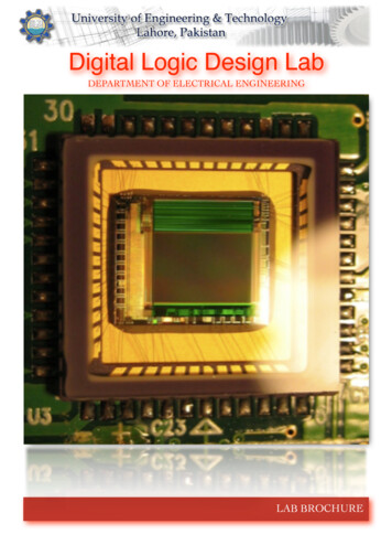
Digital Logic Design LabDEPARTMENT OF ELECTRICAL ENGINEERINGLAB BROCHURE
DIGITAL LOGIC DESIGN LABORATORYCONTENTSLab Venue. 3Lab Objectives & Courses . 3Lab Description & Experiments . 4Hardware Experiments . 5Verilog Experiments . 6Lab Resources . 7Page 2
DIGITAL LOGIC DESIGN LABORATORYObjectives & CoursesDLD Lab Venue:Computer Interfacing LabFirst Floor, Electrical DepartmentLab VenueThe Digital Logic Design Lab(DLD Lab) is one of the mostimportant and well equipped lab ofthe Department of ElectricalEngineering at University ofEngineering and Technology, Lahore.This lab is conducted at theComputer Interfacing Lab situated atthe first floor of the ElectricalEngineering Department.Scope of the LabThe DLD Lab is forundergraduate coursework related tothe course EE131. It is one of thecore modules of B. Sc. ElectricalEngineering therefore the lab has asignificant importance in thedepartment.Related CoursesThis lab is designed such that thestudents get a hands on familiaritywith the concepts they come acrossin the course EE131 that is the DigitalSystems course. This is anundergraduate course which dealswith the basics of digital systemsdesign and is a core module of theB. Sc. Electrical Engineeringcoursework as it provides theprerequisites for advance courses indigital electronics. Because of thesignificance of this course the DLDLab has been carefully designed tomeet the course requirement.Brief Overview of the LabThe Lab is well equipped withboth hardware and software facilitiesrequired by the students to performthe necessary experiments designedfor this lab. Details of the labequipment has been discussed in aproceeding section.Experiments are designed insuch a way that the students becomewell aware of the concepts they learnin the theory sessions. A list ofexperiments that are conducted inthis lab has also been mentioned in aproceeding section.Experiments are related to bothdigital hardware and VerilogProgramming.Page 3
DIGITAL LOGIC DESIGN LABORATORYLab Description & ExperimentsLab DescriptionThe Experiments in theLab have been divided intotwo major portions: Hardware Labs Hardware DescriptionLanguage (Verilog) LabsHardware Labs havebeen designed tofamiliarize students with theCombinational Digital LogicDesign and SequentialDigital Logic Designthrough the implementationof Digital Logic Circuitsusing ICs of basic logicgates and some simpledigital logic circuits.HDL (Verilog) Labs havebeen designed tofamiliarize students with theHDL based Digital DesignFlow. These labs introducestudents with differentlevels of coding available inVerilog i.e. Gate level,Dataflow level andBehavioral level. Xilinx ISE7.1 tools have been used inthese labs. Finally, theskills learnt in the HDLA Lab Demonstrationlabs are employed toimplement some digitalExpected Outcomeslogic circuits on Spartan-3With the help of the twoFPGA, using Xilinx Starterthreads of the labKit Development Board.mentioned above, studentswill have clearunderstanding of all thethree paradigms ofimplementation of digitallogic circuits: Implementation usingICs for basic logic gatesand simple circuits Implementationthrough the Developmentof Dedicated IC(ASIC) Implementationthrough ReconfigurableLogic (i.e. FPGA)This makes studentsadept in basic conceptsinvolved in digital logicdesign. The lab contributesa lot to the basic learning ofdigital systems.This shows theindispensability of theDLD Lab.List of ExperimentsList of experiments isgiven on page 5 and 6. Asmentioned before the labhas two major portionstherefore there are two listsof experiments one relatedto the hardware labs andthe other related to thehardware descriptionlanguage (verilog) labs. Allthese experiments aremandatory and each lab isfollowed by speciallydesigned assignments.A Digital Chip (inside view)Page 4
DIGITAL LOGIC DESIGN LABORATORYHardware ExperimentsTITLETOPICS1To Verify the Behavior of Logic Gates using Truth Table andFamiliarization with Digital Integrated CircuitsBasic Logic Gates,Truth Table,Integrated Circuits2Implementation of Boolean Function using Logic GatesBoolean Functions,and Introduction to Hierarchical Design of Digital Logic Circuits Boolean Algebra,Hierarchical Design of Digital Logic Circuits3Familiarization with the Different Portions of the Datasheet fora Digital IC and Using the Datasheet to Gather RelevantInformation to Utilize the IC as a Component in another DigitalLogic CircuitDatasheet of a Digital Logic IC,Hierarchical Design of Digital Logic Circuits4Implementation of 8 bit Binary Comparator using 4 bit BinaryComparatorsBinary Comparator,Hierarchical Design of Digital Logic Circuits5Implementation of 4bit into 3bit Binary Multiplier using 4bitBinary AddersBinary Multiplication,Hierarchical Design of Digital Logic Circuits6Implementation of BCD Adder using 4bit Binary Adders, 4 to 7Segment Decoder and 2Digit 7 Segment DisplayBCD addition,Hierarchical Design of Digital Logic Circuits7Implementing a Full Adder using(a) Decoder(b) MultiplexerImplementation of Boolean function usingDecoder,Implementation of Boolean function usingMultiplexer8Flip FlopsDifferent Types of Flip Flops9To study the fundamentals of basic counters and to constructvarious types of countersCountersPage 5
DIGITAL LOGIC DESIGN LABORATORYVerilog ExperimentsTITLETOPICS1Introduction to HDL based Digital Design MethodologyHDL based Digital Design Flow usingVerilog,Introduction to Outsourcing Business Model2Introduction to Basic Syntax of Verilog and Gate levelModelingthrough implementation of half adder at gate level and itssimulation using Xilinx ISE toolsBasic Concepts of Verilog, Modules andPorts, Gatelevel coding in Verilog,3Introduction to the concepts of Instantiation and HierarchicalDesign in Verilog through the implementation of full adderusing the previously designed half adder modulesHierarchical Design in Verilog4Introduction to the Concept of Vectors and Introduction toDataflow modeling through implementation of half adder andfull adder at dataflow levelVectors in Verilog,Dataflow level coding in Verilog5Consolidation of the concepts of Dataflow level modeling andIntroduction to the concept of Synthesis by the CAD toolDataflow level coding in Verilog, LogicSynthesis6Introduction to Behavioral modeling through implementation of Behavioral level coding in Veriloghalf adder and full adder at behavioral level.7Introduction to if else statement and case statement inBehavioral modeling through implementation of Multiplexerif else and case statements in Verilog8Introduction to the Concepts of Sequential Circuit anda TestBench module (Stimulus Block)Sequential circuits in Verilog, Concept ofTestbench module in Verilog9Behavioral Level Coding of Basic Sequential Circuits andConsolidation of the concepts of TestBench module (StimulusBlock)Sequential circuits in Verilog10Introduction to Field Programmable Gate Array(FPGA) andSteps involved in its ProgrammingNeed for Reconfigurable Logic, Xilinx ISETools for Programming the Xilinx FPGAsPage 6
DIGITAL LOGIC DESIGN LABORATORYLab ResourcesHardware ResourcesThe lab is fullyequipped with all thehardware required toconduct the abovementioned experiments.The hardware resources ofthe lab are: Pentium-IV PCs (withMS WinXp OS) Hardware trainers forlogic circuit design andanalysis Electronic Chips of alldigital gates Spartan-III FPGAboard kits Power SuppliesThese resources allowthe students to have ahands on experience ofbasic digital logic designconcepts. This activitygreatly leverages what thestudents learn in the theorysessions.Software ResourcesThe lab also consists ofthe software resourcesrequired by the studentsnamely:A Digital Circuit Board Veriwell ModelSimSoftware resources are Xilinx IDEequally important as Matlabhardware resources are.These software resourcesare sufficient for thestudents to performexperiments. Thesesoftwares provide thestudents with thenecessary platform to workon HDL that is the Verilog.These softwares are alsorequired to work with thesophisticated hardwareslike Spartan-III FPGAboards.The lab has all theresources whether relatedto hardware or software sothat the students becomeadept in the basic field ofdigital electronics.Students areencouraged to use the labresources to performactivities andexperiments which helpthem strengthen theirconcepts.Lab StaffLike other labs of thedepartment there is atrained and able staffconsisting of skilled labtechnicians that take careof the lab equipment.They also guidestudents about handlingthe lab equipment and theprecautionary measuresrequired for the studentswhile working in the lab.A SimulationPage 7
DIGITAL LOGIC DESIGN LABComputer Interfacing Lab1st Floor, Department of Electrical EngineeringUNIVERSITY OF ENGINEERING & TECHNOLOGY, LAHORE-54890,PAKISTAN.Ph: 92 42 9029229, Fax: 92 42 9250224url: www.uet.edu.pk
Hierarchical Design of Digital Logic Circuits 3 Familiarization with the Different Portions of the Datasheet for a Digital IC and Using the Datasheet to Gather Relevant Information to Utilize the IC as a Component in another Digital Logic Circuit Datasheet of a Digital Logic IC, Hierarchical D