Transcription
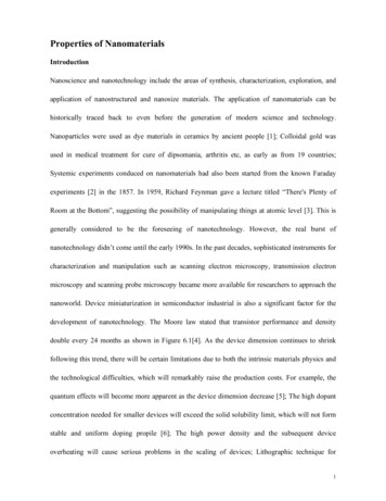
Properties of NanomaterialsIntroductionNanoscience and nanotechnology include the areas of synthesis, characterization, exploration, andapplication of nanostructured and nanosize materials. The application of nanomaterials can behistorically traced back to even before the generation of modern science and technology.Nanoparticles were used as dye materials in ceramics by ancient people [1]; Colloidal gold wasused in medical treatment for cure of dipsomania, arthritis etc, as early as from 19 countries;Systemic experiments conduced on nanomaterials had also been started from the known Faradayexperiments [2] in the 1857. In 1959, Richard Feynman gave a lecture titled “There's Plenty ofRoom at the Bottom”, suggesting the possibility of manipulating things at atomic level [3]. This isgenerally considered to be the foreseeing of nanotechnology. However, the real burst ofnanotechnology didn’t come until the early 1990s. In the past decades, sophisticated instruments forcharacterization and manipulation such as scanning electron microscopy, transmission electronmicroscopy and scanning probe microscopy became more available for researchers to approach thenanoworld. Device miniaturization in semiconductor industrial is also a significant factor for thedevelopment of nanotechnology. The Moore law stated that transistor performance and densitydouble every 24 months as shown in Figure 6.1[4]. As the device dimension continues to shrinkfollowing this trend, there will be certain limitations due to both the intrinsic materials physics andthe technological difficulties, which will remarkably raise the production costs. For example, thequantum effects will become more apparent as the device dimension decrease [5]; The high dopantconcentration needed for smaller devices will exceed the solid solubility limit, which will not formstable and uniform doping propile [6]; The high power density and the subsequent deviceoverheating will cause serious problems in the scaling of devices; Lithographic technique for1
smaller critical dimension (CD) in the range of tens of nanometers for mass production possestechnical difficulties[7]. To this point, nanotechnology may offer an alternative approach forcontinuing device scaling. Nanoelectronic devices based on new nanomaterials systems and newdevice structures will contribute to the development of next generation of microelectronics. Forexample, single electron transistor[8] [9] and field effect transistor [10-12] based on single wallcarbon nanotubes are already on the way. Proto type simple logic circuits of carbon nanotubes havealready been demonstrated [13-16].Figure 6.1 Moore law shows that the transistor performance and density doubleevery 24 months.Further, nanotechnology was also expanded extensively to other fields of interest due to thenovel properties of nanomaterials discovered and to be discovered. For example, nanowires can bepotentially used in nanophotonics, laser, nanoelectronics, solar cells, resonators and high sensitivitysensors. Nanoparticles can be potentially used in catalysts, functional coatings, nanoelectronics,energy storage, drug delivery and biomedicines. Nanostructured thin films can be used in lightemitting devices, displays and high efficiency photovoltaics. These are only a limited part of thefasting developing nanotechnology, yet numerous of other potential applications of nanomaterialshave already been or will be discovered. During the real bursting of nanotechnology in the pastdecade, nanotechnology has become a real interdisciplinary research field in which many physicists,2
chemists, biologists, materials science and other specialists are involved. Nanoinvestigations, beingwidely interdisciplinary by their very nature, promote the joining and merging of the variousscience and technology fields such as powder technology, colloid chemistry, surface chemistry andphysics, clusters and aerosols, tribology, catalysis, simulation and modeling, computer technique,etc [17].Table1.1 Typical nanomaterials [18]The term of nanomaterials covers various types of nanosturctured materials which posses atleast one dimension in the nanometer range. Table 1.1 summerized the typical nanomaterials, whichinclude zero dimension nanostructures such as metallic, semiconducting and ceramic nanoparticles;one dimension nanostructures such nanowires, nanotubes and nanorods; two dimensionnanostructures such as thin films. Besides this individual nanostructures, ensembles of thesenanostructures form high dimension arrays, assemblies, and superlattices. Nanomaterials have thestructural features in between of those of atoms and the bulk materials. While most microstructuredmaterials have similar properties to the corresponding bulk materials, the properties of materialswith nanometer dimensions are significantly different from those of atoms and bulks materials. Thisis mainly due to the nanometer size of the materials which render them: (i) large fraction of surfaceatoms; (ii) high surface energy; (iii) spatial confinement; (iv) reduced imperfections, which do notexist in the corresponding bulk mateials [19]. Due to their small dimensions, nanomaterials haveextremely large surface area to volume ratio, which makes a large fraction of atoms of the materials3
to be the surface or interfacial atoms, resulting in more “surface” dependent material properties.Especially when the sizes of nanomaterials are comparable to Debye length, the entire material willbe affected by the surface properties of nanomaterials [20, 21]. This in turn may enhance or modifythe properties of the bulk materials. For example, metallic nanoparticles can be used as very activecatalysts. Chemical sensors from nanoparticles and nanowires enhanced the sensitivity and sensorselectivity. The nanometer feature sizes of nanomaterials also have spatial confinement effect on thematerials, which bring the quantum effects. Nanoparticles can be viewed as a zero dimensionquantum dot while various nanowires and nanotubes can be viewed as quantum wires. The quantumconfinement of nanomaterials has profound effects on the properties of nanomaterials. The energyband structure and charge carrier density in the materials can be modified quite differently formtheir bulk count part and in turn will modify the electronic and optical properties of the materials.For example, lasers and light emitting diodes (LED) from both of the quantum dots and quantumwires are very promising in the future optoelections. High density information storage usingquantum dot devices is also a fast developing area. Reduced imperfections are also an importantfactor in determination of the properties of the nanomaterials. Nanosturctures and nanomaterialsfavors of a self-purification process in that the impurities and intrinsic material defects will move tonear the surface upon thermal annealing. This increased materials perfection affects the propertiesof nanomaterials. For example, the chemical stability for certain nanomaterials may be enhanced,the mechanical properties of nanomaterials will be better than the bulk materials. The superiormechanical properties of carbon nanotubes are well known.Due to their nanometer size, nanomaterials are already known to have many novel properties.Many novel applications of the nanomaterials rose from these novel properties have also beenproposed. In this chapter, the properties of nanomaterials including the mechanical, thermal,4
biological, optical and chemical properties of nanomaterials will be addressed together with thepossible applications of nanomaterials. However, due to broad coverage of the nanomaterials andrelated applications, it is nearly impossible to cover all the aspects of the nanomaterials properties inone chapter. Readers are suggested to read references [19, 22-24].Mechanical properties of nanomaterialsDue to the nanometer size, many of the mechanical properties of the nanomaterials aremodified to be different from the bulk materials including the hardness, elastic modulus, fracturetoughness, scratch resistance and fatigue strength etc. An enhancement of mechanical properties ofnanomaterials can result due to this modification, which are generally resultant from structuralperfection of the materials [19, 25]. The small size either renders them free of internal structuralimperfections such as dislocations, micro twins, and impurity precipitates or the few defects orimpurities present can not multiply sufficiently to cause mechanical failure. The imperfectionswithin the nano dimension are highly energetic and will migrate to the surface to relax themselvesunder annealing, purifying the material and leaving perfect material structures inside thenanomaterials. Moreover, the external surfaces of nanomaterials also have less or free of defectscompared to bulk materials, serving to enhance the mechanical properties of nanomaterials [19].Theenhanced mechanical properties of the nanomaterials could have many potential applications bothin nano scale such as mechanical nano resonators, mass sensors, microscope probe tips and nanotweezers for nano scale object manipulation, and in macro scale applications structuralreinforcement of polymer materials, light weight high strength materials, flexible conductivecoatings, wear resistance coatings, tougher and harder cutting tools etc.Among many of the novel mechanical properties of nanomaterials, high hardness has beendiscovered from many nanomaterials system. A variety of superhard nanocomposites can be made5
of nitrides, borides and carbides by plasma-induced chemical and physical vapor deposition [26]. Inthe appropriately synthesized binary systems, the hardness of the nanocomposite exceedssignificantly that given by the rule of mixtures in bulk. For example, the hardness of nc-MnN/a–Si3N4 (M Ti, W, V, ) nano-composites with the optimum content of Si3 N4 close to the percolationthreshold reaches 50 GPa [27-29] although that of the individual nitrides does not exceed 21 GPa.These superhard nanocomposites will have promising potential in hard protective coatings.Superhardness also comes from pure nanoparticles. For example, Gerbericha report thesuperhardness from the nearly spherical, defect-free silicon nanospheres with diameters from 20 to50 nm of up to 50 GPa, fully four times greater than the bulk silicon [30].Since their discovery [31, 32], carbon nanotubes have stimulated intensive research interests. As thesmallest carbon fibers discovered, carbon nanotubes have been found to have excellent mechanicalproperties. The strength of the carbon fibers would increases with graphitization along the fiber axis.Carbon nanotubes, which are formed of seamless cylindrical graphene layers, represent the idealcarbon fiber and should presumably have the best mechanical properties in the carbon fibers species,showing a high Young’s modulus and high tensile strength [33]. Theoretical research has predictedthe high modulus of carbon nanotubes aside from the direct experimental measurement, whichcalculated the Young’s moduli Y of single wall carbon nanotubes to be from 0.5-5.5TPa, muchhigher than high-strength steel of 200 GPa [34, 35]. The Young’s moduli and the tensile strengthhave also been measured experimentally [33, 36-39]. The first experimental measurement ofYoung’s modulus of Multiwall carbon nanotubes was obtained by measuring thermal vibrations ofcarbon nanotubes using transmission electron microscopy (TEM), yielding the Young’s modulus of1.8 /-0.9 TPa [38]. In this method, the amplitude of the thermal vibrations of the free ends as afunction of temperatures of anchored nanotuebes was correlated with the young’s modulous. Figure6
1.2 shows the free standing multi wall carbon nanotubes with tip blurring due to thermal vibration.Figure 1.2: the free standing multi wall carbon nanotubes with tip blurring due to thermal vibration.By using a similar technology, Krishnan measured the young’s modulous of single wall carbonnanotubes, resulting in average value of Y 1.25 -0.35/ 0.45 TPa [33]. Atomic force microscope(AFM) has also been employed to measured the young’s modulus of the carbon nanotubes [39].This is realized by bending the anchored carbon nanotubes with AFM tip wihle simultaneouslyrecording the force by the tube as a function of the displacement from its equilibrium position. Theresultant Young’s modulous was 1.28 /- 0.5 TPa. The values of Young’s moduli measured fromdifferent ways were all in the range in theorical prediction, proving the existence the high elasticmodulus of the carbon nanotubes. The tensile strength of carbon nanotubes has also been measured[36, 37].7
Figure 1.3: A multi wall carbon nanotube was aligned between two AFM tips. The lower AFM tipis on a soft cantilever whose deflection is recorded to determine the force applied on the carbonnanotube.An individual multi wall carbon nanotube was mounted between two AFM tips, one on rigidcantilever and the other on soft cantilever (Figure 1.3). By recording the whole tensile loadingexperiment, both the deflection of the soft cantilever from which the force applied on the nanotubeand the length change of the nanotube were simultaneously obtained. The carbon nanotubes brokein the outermost layer (“sword-in-sheath” failure), and the tensile strength of this layer ranged from11 to 63 GPa and the measured strain at failure can be as high as 12%. For comparison, the tensilestrength of high-strength steel is 1-2 GPa [36, 37].The excellent mechanical properties of nanomaterials could lead to many potential applications inall the nano, micro and macro scales. High frequency electro-mechanical resonators have beenmade from carbon nanotubes and nanowires.8
Figure 1.4 (a) SEM image showing the carbon nanotubes suspended between two electrodes(top). The schematic de vice geometry is shown at the bottom. Scale bar: 300 nm [40]. (b) SEMimage of the resonator with a suspended nanowire.An individual carbon nanotube was contacted with two metal electrodes and was doubly clampedand suspended across a trench, which was realized by conventional lithography technique (Figure1.4). The nanotube resonator was actuated and detected through electrostatic interaction using backside gate electrode underneath the tube in a vacuum. The guitar-string-like oscillation modes ofdoubly clamped nanotube was discoved from the resonator with the resonant frequency as high as55 MHz. A similar nanoelectromechanical resonator can also be fabricated from platinumnanowires [41]. The nanowire resonator bear a similar but a with side gate electrode to detect theactuation [40], which gave a resonant frequency of 105MHz. These NEMS oscillators couldpotentially useed in ultrasensitive mass detection1, radio-frequency signal processing, and as a9
model system for exploring quantum phenomena in macroscopic systems.Nano structured materials can also be used as nanoprobes or nanotwizzers to probe and manipulatenanomatierals in a nanometer range [42-46]. Due to their high aspect ratio and small dimensions,one-dimension nano structures such as carbon nanotubes can also be used as nano probe tips. Daiattached multi wall carbon nanotube to conventional pyramidal tip of a silicon cantilever forscanning force microscopy [43].Figure 1.5: SEM image of a MWNT attached on the silicon cantilever tip [44].Table 1.2 The comparasion of the Resolution Obtained with Nanotube and Silicon Tips on A‚40Fibrils and Protofibrils [44].Stanislaus S. Wong acquired high resolution AFM image for biological systems by using carbonnanotubes tips[42, 44]. Figure 1.5 shows a typical nanoprobe tip made from carbon nanotube. Whilemost conventional tips suffer from “tip crash”, posse significant constraints on potential lateralresolution, and furthermore, the large probe size restricts the ability of these tips to access narrow10
and deep features. Probe tips from carbon nanotubes could offer several advantages: the flexibilityof carbon nanotubes makes the tip more resistant to damage from tip crashes; the high aspect rationof carbon nanotubes makes them suitable to image sharp recesses in surface topography; Tips fromcarbon nanotubes could significantly improved lateral resolution; carbon nanotubes tips are morerobust and less prone to contamination. By investigating the amyloid-β1-40 (Aβ40) fibrils underAFM, Stanislaus compared the performance of nanotubes tips and the single crystal silicon tips(Table 1.2) An improvement of the image resolution (smaller fibrils and protofibrils with wereimaged using carbon nanotube tips) due to a reduction of the effective tip radii when imaging withnanotube tips was acquired [44].Similar to the carbon nanotube nanoprobe fabrication, if on the supporting micro structure, twoindividual carbon nanotubes are attached instead of only one nanotube in case of nanoprobe, then ananotube nano tweezers would result. Phillip Kim showed such a nanotube tweezers by attachingtwo carbon nanotubes on glass micropipettes [45]11
Figure 1.6 Dark field optical images of the electro-actuated nanotube nanotwizzers.This nano tweezers operated under electrical stimulus and was used to probe the electricalcharacteristics of nanostructures. It could be useful both in the nanostructure characterization andthe manipulation. The nanotweezers could be used as a novel electromechanical sensor that candetect pressure or viscosity of media by measuring the change in resonance frequency and Q-factorof the device. They can also be explored into manipulation and modification of biological systemssuch as structures within a cell.The enhancements of mechanical properties of polymeric materials by nanofillers are also veryactive applications of nanomaterials. Micrometer size fillers were used in traditional polymercomposites and showed improvements in their mechanical properties such as the modulous, yieldstrength and glass transition temperature [47, 48]. However, these performacen enhancements will12
sacrifice the ductility and toughness of the materials and large amounts of filler were needed toachieve the desired properties. Comparably, polymer nanocomposites from nano size fillers couldresult in unique mechanical properties at very low filler weight fractions [49]. Sumita founddramatic improvements in the yield stress (30%) and Young’s modulus (170%) in polypropylenefilled with with ultrafine SiO2, compared to micrometer-filled polypropylene [50].Ou et al. fillednylon-6 with 50 nm silica particles using in situ polymerization method. They reported increases intensile strength (15%), strain-to-failure (150%), Young’s modulus (23%), and impact strength (78%)with only 5 wt % nanoparticles content [51]. Petrovic found a 6 times increase in theelongation-at-break and a 3 times increase in the modulus in a rubbery polyurethane elastomer filledwith 40 wt % 12 nm silica, compared to a micrometer-sized filler reinforced polymer [52].Vinylacetate, acrylic ester, synthetic rubber, and other polymer latexes have been used in coatingsand adhesives; colloidal silica is used with these polymer emulsions in order to improve adhesion,durability, and abrasion resistance. The silica also serves to prevent stickiness and improves thewashing resistance of the coatings [53]. Besides nanoparticles, One-dimension nanostructures suchas carbon nanotubes are also superior candidates for nano fillers because of their high aspect ratioand excellent mechanical properties. Nanocomposite materials from carbon nanotubes are expectedto exhibit outstanding mechanical properties, such as high Young’s modulus, stiffness andflexibility.13
Table 1.3 Comparative results (E , % increase E ) of CNTs composites obtained in differentpolymer matrices at 40 C 1Hz of frequency [54].Table 1.3 summarized some results from several research groups of the enhancement of mechanicalproperties of polymers nanocomposites containing carbon nanotubes fillers [54-59]. Without the useof additives, generally more than 100% in “E ” was acquired. Besides the improvement ofmechanical properties in carbon nanotube- polymer nanocomposites, they can further be employedas multifunctional materials providing light weight, strong and tough structural materials as well asexcellent electrical conducting and thermal conducting properties.Thermal properties of nanomaterialsThe recent advances of nanotechnologies in the past decades have resulted in the burst of promisingsynthesis, processing and characterization technologies, which enables the routine production of avariety of nanomaterials with highly controlled structures and related properties. By controlling thestructures of nanomaterials at nano scale dimensions, the properties of the nanostructures can becontrolled and tailored in a very predictable manner to meet the needs for a variety of applications.Examples of the engineered nanostructures include metallic and non-metallic nanoparticles,nanotubes, quantum dots and superlattices, thin films, nano composites and nanoelectronic andoptoelectronic devices which utilize the superior properties of the nanomaterials to fulfill theapplications.Many properties of the nanoscale materials have been well studied, including the optical electrical,magnetic and mechanical properties. However, the thermal properties of nanomaterials have onlyseen slower progresses. This is partially due to the difficulties of experimentally measuring andcontrolling the thermal transport in nano scale dimensions. Atomic force microscope (AFM) has14
been introduced to measure the thermal transport of nanostructures with nanometer-scale highspatial resolution, providing a promising way to probe the thermal properties with nanostructures[60]. Moreover, the theoretical simulations and analysis and of thermal transport in nanostructuresare still in infancy. Available approaches including numerical solutions of Fourier’s law,computational calculation based on Boltzmann transport equation and Molecular-dynamics (MD)simulation, all have their limitations [60]. More importantly, as the dimensions go down intonanoscale, the availability of the definition of temperature is in question. In non-metallic materialsystem, the thermal energy is mainly carried by phonos, which have a wide variation in frequencyand the mean free paths (mfp). The heat carrying photons often have large wave vectors and mfp inthe order of nanometer range at room temperature, so that the dimensions of the nanostructures arecomparable to the mfp and wavelengths of photons. However the general definition of temperatureis based on the average energy of a material system in equilibrium. For macroscopic systems, thedimension is large enough to define a local temperature in each region within the materials and thislocal temperature will vary from region to region, so that one can study the thermal transportproperties of the materials based on certain temperature distributions of the materials. But fornanomaterial systems, the dimensions may be too small to define a local temperature. Moreover, itis also problematic to use the concept of temperature which is defined in equilibrium conditions, forthe nonequilibrium processes of thermal transport in nanomaterials, posing difficulties fortheoretical analysis of thermal transport in nano scales [60].In spite of all the difficulties in both experimental and theoretical characterization the thermalproperties of nanomaterials. Recent advances in experiments have showed that certainnanomaterials have extraordinarily thermal properties compared to their macroscopic counterparts,as will be explained in detail in this section. In nanomaterials systems, several factors such as the15
small size, the special shape, the large interfaces modified the thermal properties of thenanomaterials, rendering them the quite different behavior as compared to the macroscopicmaterials. As mentioned above, as the dimension goes down to nano scales, the size of thenanomaterials is comparable to the wavelength and the mean free path of the photons, so that thephoton transport within the materials will be changed significantly due the photon confinement andquantization of photon transport, resulting in modified thermal propeties. For example, nanowiresfrom silicon have a much smaller thermal conductivities compared to bulk silicon [61]. The specialstructure of nanomaterials also affects the thermal properties. For example, because of it tubularstructures of carbon nanotubes, they have extreme high thermal conductivity in axial directions,leaving high anisotropy in the heat transport in the materials [62]. The in interfaces are also veryimportant factor for determine the thermal properties of nanomaterials. Generally, the internalinterfaces impede the flow of heat due to photon scattering. At interface or grain boundary betweensimilar materials, the interface disorder scatters phonons, while as the differences in elasticproperties and densities of vibrational states affect the transfer of vibrational energy acrossinterfaces between dissimilar materials. As a result, the nanomaterials structures with highinterfaces densities would reduce the thermal conductivity of the materials [63]. Theseinterconnected factors joined together to determine the special thermal properties of thenanomaterials. Thermal properties of several nanomaterials systems and their possible applicationswill be discussed below.As the first example, carbon nanotubes are carbon nanostructures relating to diamond andgraphite, which are well known for their high thermal conductivities. The stiff sp3 bonds in diamondstructure result in high phonon speed and consequently high thermal conductivities of the material.In carbon nanotubes, the carbon atoms are held together by the even stronger sp2 bonds, so that the16
nanotube structures, consisting of seamlessly joined graphitic cylinders are expected to haveextraordinarily high thermal conductivities. The rigidity of the these nanotubes, combined withvirtual absence of atomic defects or coupling to soft photon modes of the embedding medium,should make isolated nanotubes very good candidates for efficient thermal conductors [64]. Thehigh thermal conductivity of carbon nanotubes were first proved by some theoretical calculations[64, 65]. Savas Berber et al combined the equilibrium and nonequilibrium molecular dynamicssimulations with Tersoff potential to determine the thermal conductivity of carbon nanotubes and itsdependence on temperature.Figure1.7 Temperature dependence of the thermal conductivity for a (10, 10) carbon nanotubefor temperatures below 400 K [64].They concluded that the thermal conductivity of an isolated (10, 10) nanotubes was dependent onthe temperature and an extraordinarily high value of 6600W/mK was resultant at roomtemperature, shown in Figure 1.7. This is comparable to the thermal conductivity of a hypotheticalisolated graphene monolayer or diamond. From the thermal conductivity of bulk carbon nanotubesamples, J. Hone, et al estimated the thermal for a single tube to be 1800 - 6000 W/mK at roomtemperature [66]. Che et al also used equilibrium molecular dynamics simulations to calculatecarbon nanotubes' thermal conductivities and gave a thermal conductivity of 2980 W/mK along17
the tube axis for a (10, 10) nanotube [67]. In spit of the discrepancies of the values from thesetheoretic works, nonetheless, it showed that carbon nanotubes have high thermal conductivities.Experimental work has also been performed to measure the thermal conductivities of single carbonnanotubes or small nanotube bundles [68, 69].Figure 1.8: the thermal conductance of an individual MWNT (d 14 nm). Lower inset: Solid linerepresents thermal conductivity of an individual MWNT (d 14 nm). Broken and dotted linesrepresent small (d 80 nm) and large bundles (d 200 nm) of MWNTs, respectively. Upper inset:SEM image of the suspended islands with the individual MWNT. The scale bar represents 10 mm[68].P. Kim et al measured the thermal conductivity of an individual carbon nanotube by attaching singlenanotube or small bundles to the microfabricated suspended devices as shown in Figure 1.8, andreported the thermal conductivity of above 3000W/mK for a single nanotube at room temperature.Recently Motoo Fujii et al measured the thermal conductivity of single carbon nanotube using asuspended sample-attached T-type nanosensor [69], and reported values exceeding 2000W/mK fora carbon nanotube of 9.8nm diameter. These experimental values were in the range of the18
theoretical calculations, proved the high thermal conductivity of the carbon nanotubesexperimentally. Due to their high thermal conductivities, carbon nanotubes or nanotubes basednanocomposite could be promising candidates for heat transport management in many applicationssuch as in the integrated circuits, optoelectronic devices and MEMS structures.On the other hand, one-dimensional nanowires may offer ultra low thermal conductivities, quitedifferent from that of carbon nanotubes. In nanowires, phonons behave differently from those in thecorresponding bulk materials due to the quantum confinement in the one dimension structures. Thenanowire surface can introduce surface phonon modes, resulting in many different phononpolarizations other than the two transverse and one longitudinal acoustic branches found in bulksemiconductors. Those changes in the dispersion relation can modify the group velocity and thedensity of states of each branch. The phonon lifetime also changes due to the strong phonon–phonon interactions and the boundary scattering within the nanostructures [60]. Thus the phonontransports and the thermal properties of the nanowires will be significantly different from that of thebulk materials. The phonon transport of semiconducting nanowires have been studiedexperimentally [61, 70] and theoretically [71-73]. Deyu et al measured the thermal conductivity ofsilicon nanowires using a
confinement of nanomaterials has profound effects on the properties of nanomaterials. The energy band structure and charge carrier density in the materials can be modified quite differently form their bulk count part and in turn will modify th