Transcription
OPTICAL PROPERTIESof NanomaterialsAdvanced ReadingOptical Properties and Spectroscopy of NanomaterialsJin Zhong ZhangWorld Scientific, Singapore, 2009.
Optical Properties Many of the optical properties are closely related to the electrical and electronicproperties of the material. But as we shall see other factors also come into thepicture when dealing with optical properties. When one is talking about optical properties, one is usually referring to theinteraction of electromagnetic radiation with matter. The simple picture one canstart with is by considering a 'ray' of an electromagnetic wave of a singlefrequency entering a medium from vacuum. This ray could be reflected,transmitted (refracted) or absorbed. The reflection could be specular or diffuse.
From a more fundamental perspective, there are only two possibilities (of interaction of amedium with electromagnetic radiation):(i) scattering &(ii) absorption If one considers a wider spectrum of frequencies, then some part of the spectrum could beabsorbed while the other frequencies could be scattered.
Absorption essentially involves activating some process in the material to take it to anexcited state (from the ground state).These processes are: (i) electronic, (ii) vibrational and (iii) rotational excitations Further part of the absorbed energy could be re-emitted. If the absorbed energy is dissipated as heat, this is called dissipative absorption.Atomic orbitalsElectronic transitionsMechanismsVibrational transitionsfor absorptionRotational transitionsMolecular orbitalsBand
When an electromagnetic wave impinges on an atom (or a material containing an atomicspecies), the electron cloud is set into oscillation. This situation is like a dipole oscillator,which emits radiation of the same frequency in all directions. This is the process ofscattering. Similar to absorption, scattering is also frequency dependent. There are two possible ways in which transmission can take place:(i) if the medium is sparse, the ray (wave) could just pass through the particles of themedium (like in vacuum), which essentially means there is no interaction;(ii) but the more common mechanism for 'denser media' is 'forward scattering' (i.e. whatwe call as transmission in common usage is actually forward scattering). When a wave is being transmitted form one medium (say vacuum) to another, itsfrequency remains constant, but its velocity decreases (the wave being slower in themedium). The ratio of the velocities c/vmedium is called the refractive index (n):n c KE KM 0 0v 0 KM 0KE Where, is permittivity of the medium and is the permeability of the medium. The subscript'0' refer to these values in vacuum. KE is the relative permittivity (dielectric constant) and KMis the relative permeability of the medium.
Usually KM is close to unity. KE is a function of the frequency of the electromagneticwave and leads to the phenomenon of dispersion (e.g. dispersion of white light by a prisminto 'VIBGYOR' colours). Physically, the origin of the dependence of 'n' on frequency is due to three factors:(i) orientational polarization(ii) electronic polarization(iii) ionic polarization(iv) space charge.
Usually the refractive index (n) is greater than one (n 1), but under certaincircumstances it can be less than one (n 1) or even be negative (n 0). n 1 implies that light is traveling faster than speed of light which is in 'apparent'contradiction to the theory of Relativity. In cases where n 1, the velocity which one needs to consider (instead of the 'phasevelocity') is the 'group velocity (vg)' (or in still other cases the 'signal velocity' (vs)), whichwill be less than 'c'. [i.e. causality will not be violated!]. In negative refractive index materials (or typically structures) the refracted beam (in themedium) will be on the other side of the normal.
A special kind of scattering of importance to materials science is diffraction. Diffraction isnothing but 'coherent reinforced scattering' and comes into play in periodic andquasiperiodic structures. The incoming 'coherent beam' (assumed monochromatic fornow) energy is redistributed in space as 'transmitted' and diffracted beams. Thetransmitted beam in this case is a forward diffracted beam. If there are an array of scatters(1D) with spacing 'a', a schematic of dominant regimes of the three possible outcomeswhich can take place. Though in our discussions here we have considered EM waves, phenomena such asscattering and diffraction are true for all kinds of waves. Young's double slit experimentperformed in a ripple tank (with water as the medium) is a good example of scattering andinterference, which does not involve EM radiation.
Origin of Colour Colour can arise from various mechanisms as outlined igin of colourScattering Blue skyDispersion PrismInterference Oil films on water, CD,Butterfly wing2.105 eV2.103 eV3p589.1 nm589.6 nm3s Atomic electronic transitions can give rise to colour: yellow colour of sodium in flame test
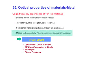
Interaction of electromagnetic radiation with metals: Absorption in metals Plasmons (akin to phonons for lattice vibrations) are collective oscillations of free electrons. Bulk plasmons are longitudinal oscillations of electrons gas w.r.t. the ion cores. Incoming visible electromagnetic radiation sets up plasmon oscillations and hence isabsorbed (bulk metals are opaque in the visible region).
Three (two, sub-divided into three) frequency regimes can be identified for interaction ofEM radiation with metals.Au Pt Al Ag P (1015 /s) 2.18 1.24 3.57 2.18 1) Low frequency range ( 1) beam penetrates the metal for a short distance (skindepth) below the surface. (for Cu at 107 /s, 100 ) absorbed (& reflected) 2) High frequency range ( 1 visible and ultraviolet range)Ne 2 P a) P reflection Lattice m* a) P metal becomes a non-absorbing transparent dielectric time between two consecutive collisions. 10 14 s. 1/ probability of an electron suffering a collision/unit time P plasma frequency N electron density
Optical properties of semiconductors Ionic crystals show strong absorption and reflection in the IR region(due to interaction of light with optical phonons). Compound semiconductors (GaAs, GaP etc.) have a partial ioniccharacter to their bond and exhibit absorption and reflection in theIR. If energy of the incoming photon is greater than the band gap thenthe photon can be absorbed. h Eg 0 Eg/h is known as theabsorption edge. As the wave vector of a photon in the optical region is very small(only constant momentum transfers are allowed across the bandgap) vertical transitions in k-space are allowed (valence to conductionband). As the bandgap in semiconductors is 1eV the fundamental edgeoccurs in the IR. In indirect bandgap semiconductors both photon and phonon needsto be absorbed (the phonon energy 0.05eV and can be ignored andhence it can be thought of as contributing only momentum to theelectron).
Exciton Exciton is a bound state of an electron and hole. The binding is due to electrostatic(Coulomb) attraction the exciton has lower energy than the unbound electron hole. This brings the energy levels closer to the conduction band (and the Bohr radiusincreases) It is an electrically neutral quasiparticle that exists in insulators and semiconductors. The exciton can be considered as an elementary excitation in materials which cantransport energy without transporting electric charge (excited state can travel throughlattice without transfer of charge). [The free exciton (Mott-Wannier) can move in the crystal.Exciton trapped by an impurity is a bound exciton (has a higher binding energy than freeexciton)]. The effective reduced mass of exciton ( ):For GaAs:* excitonme* mh* *me mh** exciton 0.059me me* effective mass of electron mh* effective mass of hole(this is much smaller thanthe free electron mass me)
Photon absorption by a semiconductor can lead to the formation of an exciton. The exciton binding energy for most semiconductors is in the range of few to few 10s ofmeV (milli-electron volts) [Eexciton(GaAs) 4.6 meV, Eexciton(CdS) 28 meV] .For comparison: the binding energy of H2 atom is 13.6 eV and kT at room temperature is 40 meV. Given the small value of Eex an exciton can be dissociated by thermal energy at RT. The exciton spectrum has a sharp line, just below the fundamental edge usuallyobserved at low temperature where thermal energy is lower than the binding energy.Small 0.01 eVh Eg Eexciton
The exciton diameter can be calculated as:ExcitonBohrrExcitonBohrr rB me [1 (me* / mh* )] 0 me* 0 h2 e2 rB Bohr radius in the absence of exciton dielectric constant of the medium 0 dielectric constant of free space me mass of free electron me* effective mass of electron mh* effective mass of holeExciton radius hasnanoscale dimensionsExcitonExcitonenergy (meV) radius (nm)GaAs4.6CdSeCdS28Band-Gapenergy (eV) 11.81.43 51.74 3 (2.4)2.58Hydrogen atom ground state: 13.6 eV If the dimension of the crystal of the exciton diameter (or less) confinement effects become prominent.Small 0.01 eV
Optical Properties of Nanomaterials
Size effect on optical properties Bulk metal samples absorb electromagnetic radiation (say visible region). Thin films ofmetals may partially transmit, just because there is insufficient material to absorb theradiation. Au films few 10s of nm thick become partially transparent. Apart from ‘insufficient material’ effects, there are important phenomena which come intoplay in nanomaterials. These include: dominance of surface plasmons, quantum confinement effects, etc. E.g. in semiconductor quantum dots optical absorption and emission shift to the blue(higher energies) as the size of the dots decreases. The size reduction is more prominent in the case of semiconductors as compared to metals(i.e. quantum size confinement effects become more important in metals at smaller sizesthan semiconductor crystals). We have already seen that at very small sizes metal nanoparticles can develop a bandgap(can become a semiconductor or insulator).
Semiconductor nanoparticles & films On decreasing the size the electron gets confined to the particle (confinement effects)leading to:(i) increase in bandgap energy and(ii) band levels get quantized (discrete). Surface states (trap states), which lie in the bandgap become important alter the opticalproperties of nanocrystals. The energy level spacing increases with decreasing dimension Qunatum Size Confinement Effect
The effective bandgap of particle of radius R:Eeffectiveg 2 2 11 1.8e 2( R ) E g ( ) * 2 *2 R me mh RR Egeffective this dominates overR Egeffective R Egeffective (Coulombic attraction term) Egeffective effective band gap energy of particle of radius R Eg( ) bulk bandgap dielectric constant (bulk) me mass of free electron me* effective mass of electron mh* effective mass of hole
GaAs nanocrystalline thin film (nano-GaAs)deposited on ITO substrate In nano-GaAs (with size range 7-15 nm) a broad excitonic peak at 526.0 nm (2.36 eV) isseen energy gap of the nano-GaAs has been blue shifted by 0.93 eV [bulk band gap (1.43eV)] due to the QSE. Enhancement of absorbance over the range of wavelengths seen enhanced oscillatorstrength (dimensionless quantity to express the strength of the transition). The excitonic peak is broad due to the size distribution of crystallites.J. Nayak et al., Physica E 24 (2004) 227–233
With reducing size of the particle the density of states becomes more quantized and the bandgap shifts to higher energies (shorter wavelengths) the absorption spectrum shows a blueshiftAbsorption spectra of PbSe nanocryatals
Photoluminescence In photoluminescence material is excited by EM radiation, followed by relaxation toground state by emission of photons. When the semiconductor relaxes to the ground state by recombination of electron andhole, a photon is emitted. If the photon energy lies in the range 1.8 - 3.1 eV the radiation will be in the visible range luminescence. By changing the size of the nanoparticles the frequency of emission can be tailored. As the size of the nanoparticles decrease ‘blue shift’ in frequencies.
Properties of core-shell nanostructures: semiconductor on semiconductor The luminescent properties are a characteristic of the core. The shell leads to an enhancement of the luminescent properties of the core (theluminescence of nanoparticles are well defined with narrow spectral ranges, which dependon particle size). Deposition of a semiconductor with a larger bandgap than that of the core typically resultsin ‘luminescence enhancement’ due to the suppression of radiationless recombinationmediated by surface states. E.g. CdS coated with MoS4, ZnSe coated with CdSe, CdSe coated with CdS.Bandgaps tunable in the near-IR, which can be useful as IR biological luminescentmarkers.
Fluorescence from core-shell quantum dotsZnS CdSeFluorescence emission of (CdSe)ZnS coreshell quantum dots.Dabbousi et al., J. Phys. Chem. B 1997, 101, 9463-9475
Colour of metallic nanoparticles Gold nanoparticles were used as a pigment of ruby-colored stained glass dating back tothe 17th century. 1-10 nm sized particles give rise to this colour. Thin film of Au ( 100nm or less) will transmit blue-violet light. The colour of metallic nanoparticles depends on size in the nanoscale regime. Bulk Au is ‘golden’ yellow colour. Nanoparticles of gold (colloidal) can have red, purpleor blue colour.The colour depends on the size (& shape) of the particle and the dielectric properties ofthe medium. Surface plasmons are excited by incident electromagnetic radiation. Surface plasmons have lower energy than bulk plasmons which quantize the (or plasma). MFP of Au, Ag 50 nm for particles smaller than this there will be no scattering withinthe particle and all the interactions will be with the surface. In particles with shape anisotropy (e.g. cylinders) more than one type of plasmonabsorption peak may be observed.
For the sphere (d 15nm) only the Transverse plasmon peak is observed ( 520nm). If the radius of the sphere is doubled (d 30nm), the transverse plasmon absorption peakwill only shift slightly this is unlike semiconductor nanoparticles where the absorbanceis strongly affected by size in the nanoscale. For the cylinder both the surface and longitudinal plasmon peaks are observed. For the longer cylinder the longitudinal plasmon peak shifts to longer wavelengths. Many applications has been envisaged due to large enhancement of surface electric field.
Properties of core-shell nanostructures: metal on dielectric In Au shells coated on SiO2 cores the plasmon band depends on the core radius and on thecore to shell ratio. Increasing core to shell ratio red-shifts the plasmon resonance band (figure below).After: S. J. Oldenburg, R. D. Averitt, S. L. Westcott, N. J. Halas, Chem. Phys. Lett. 288, 243 (1998)
Metamaterials (with negative refractive index) Negative index metamaterials (negative index materials) are man made structures wherethe refractive index has a negative value (typically over some frequency range). So far this has not been discovered in natural materials. Metamaterials have been made with negative effective permittivity and permeability. A crystal with Magnetic Split Ring Resonator (SRR) as the motif can be used for theconstruction of a negative refractive index material. When the SRR scale is of the order of 200nm negative refractive index can beobtained in the mid-infrared range (100 THz)n ( ) ( ) Refractionn n ( ) ( ) Refraction
End of Course
Properties of core-shell nanostructures: dielectric or semiconductor on metal SiO2 shell on various cores have been studied. E.g. Au@SiO2. Core shell nanowires have also been prepared. E.g. Ni@TiO2. Au@SiO2: Nanosized gold colloids show a very intense surface plasmon absorption bandin the visible (around 520 nm). The exact position of this plasmon band is extremelysensitive both to particle size and shape and to the optical and electronic properties of themedium surrounding the particles. Silica does not exchange charge with the Au particlesand hence can be considered inert.As the shell thickness is increased, there is an increase in the intensity of the plasmonabsorption band, as well as a red shift in the position of the absorption maximum (due tothe increase in the local refractive index around the particles). At larger shell thicknesses,scattering becomes significant, resulting in a strong increase in the absorbance at shorterwavelengths. This effect promotes a blue shift of the surface plasmon band and aweakening in the apparent intensity of the plasmon band. Eventually at shell thicknessesabove 80 nm, the scattering almost completely masks the surface plasmon band.Au core, SiO2 shell.Constant core diameter,increasing shelldiameter.Core shell nanowire
Properties of core-shell nanostructures: metal on metal Examples: Au@Ag, Au@Pb, Au@Sn, Ag@In. Metal nanoparticles display very interesting optical and electronic properties. These arise due to the collective oscillation of conduction electrons, when interacting withan electromagnetic radiation (of certain frequency). Surface plasmon resonance frequency is the relevant property. Formation of core-shell structures alters the property of the pure metal. E.g.: Pure Au has an plasmon absorption frequency of 518nmSilver coating blue shifts and broadens the absorption peak. The peaks shifts to 400nm forsufficiently thick Ag shells.Coated magnetic nanoparticles The shell usually stabilizes the core (also in colloidal form). The core gives rise to the relevant properties. Fe@Au nanoparticles show superparamagnetic behaviour. Fe@Nd shows low coercivities.
When an electromagnetic wave impinges on an atom (or a material containing an atomicspecies), the electron cloud is set into oscillation. This situation is like a dipole oscillator,which emits radiation of the same frequency in all directions. This is the process ofscattering. Similar to absorption, scattering is also frequency dependent. There are two possible ways in which transmission can take place:(i) if the medium is sparse, the ray (wave) could just pass through the particles of themedium (like in vacuum), which essentially means there is no interaction;(ii) but the more common mechanism for 'denser media' is 'forward scattering' (i.e. whatwe call as transmission in common usage is actually forward scattering). When a wave is being transmitted form one medium (say vacuum) to another, itsfrequency remains constant, but its velocity decreases (the wave being slower in themedium). The ratio of the velocities c/vmedium is called the refractive index (n):c KE KMn 0 0v 0 KM 0KE P e ED ( E P)B 0 (H M) BH MHWhere, is permittivity of the medium and is the permeability of the medium. The subscript'0' refer to these values in vacuum. KE is the relative permittivity (dielectric constant) and KMis the relative permeability of the medium.
With reducing size of the particle the density of states becomes more quantized and the bandgap shifts to higher energies (shorter wavelengths) the absorption spectrum shows a blueshift When the particle radius is few times the exciton radius the exciton levels decide theenergy levels When the dimension of the particle is exciton radius exciton ceases to exist.Eexciton 13.6 / me eV2 2 ( / 0 ) n n 1 lowest energy ground state Eexciton exciton binding energy dielectric constant of the medium 0 dielectric constant of free space me mass of free electron me* effective mass of electron mh* effective mass of hole n quantum number (n corresponds to unbound state)
Variation of Emission spectra ofCdSe quantum dots with size
Many of the optical properties are closely related to the electrical and electronic properties of the material. But as we shall see other factors also come into the picture when dealing with optical properties. When one is talking about optical properties, one is usually referring to