Transcription
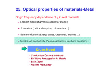
25. Optical properties of materials-MetalDrude Model Conduction Current in MetalsEM Wave Propagation in MetalsSkin DepthPlasma Frequency
Drude modelz Drude model : Lorenz model (Harmonic oscillator model) without restoration force(that is, free electrons which are not bound to a particular nucleus)Remind! Linear Dielectric Response of Matter
ConductionConduction CurrentCurrent inin MetalsMetalsThe equation of motion of a free electron (not bound to a particular nucleus; C 0),m drd2r eEme 2 C r eτ dtdtLorentz model(Harmonic oscillator model) meIfC 0dv me γ v e Edt(τ Drude model(free-electron model)The current density is defined :C AJ N ev 2 s im 2 mSubstituting in the equation of motion we obtain : N e2 dJ γJ Edt me 1γ: relaxation time 10 14 s)
N e2 dJ γJ Edtm e Assume that the applied electric field and the conduction current density are given by :E E0 exp ( i ω t )J J 0 exp ( i ω t )Local approximationto the current-field relationSubstituting into the equation of motion we obtain :d J 0 exp ( i ω t ) dt γ J 0 exp ( i ω t ) i ω J 0 exp ( i ω t ) γ J 0 exp ( i ω t ) N e2 E0 exp ( i ω t ) me Multiplying through by exp ( i ω t ) : N e2 ( i ω γ ) J 0 E0 ,m e or equivalently N e2 ( i ω γ ) J E me
N e2 ( i ω γ ) J E me For static fields (ω 0 ) , N e2 J E σ E , whereγm e N e2σ : static conductivitymeγFor the general case of an oscillating applied field : N e 2 / meσσ J : dynamic conductivity E σ ω E , where σ ω ωγωγγω i1/1/ii()() For very low frequencies, (ω γ ) 1,the dynamic conductivity is purely real and the electrons follow the electric field .As the frequency of the applied field increases, the inertia of electrons introducesa phase lag in the electron response to the field , and the dynamic conductivity is complex.( )For very high frequencies, (ω γ ) 1, J i σ E e 2 σ Eiπthe dynamic conductivity is purely imaginaryand the electron oscillations are 90 out of phase with the applied field .
PropagationPropagation ofof EMEM WavesWaves inin MetalsMetalsMaxwell ' s relations give us the following wave equation for metals :1 2 E1 J E 2 2 c tε 0 c 2 t2P 0, J 0 σBut , J E 1i/ωγ) (Substituting in the wave equation we obtain :1 2 E1 E 2 2 c tε 0 c22 Eσ iωγ1/() tThe wave equation is satisfied by electric fields of the form :()E E0 exp i k r ωt k 2 σ ω μ0 i ,c2i/ 1ωγ() ω2where c 2 1ε 0 μ0
SkinSkin DepthDepth atat lowlow frequencyfrequencyConsider the case where ω is small enough that k 2 is given by :k 2 σ ω μ0 π iiexpσωμ 0 i σ ω μ0c2i1/ωγ () 2 ω2Then , k σ ω μ0 π π π π exp i σ ω μ0 exp i σ ω μ0 cos i sin σ ω μ0 (1 i )2 2 4 4 4 kR kI σ ω μ02 σ c 2 μ0 2ω c nR nI k R , I ω σ2ωε 0In the metal , for a wave propagating in the z direction : z E E0 exp ikz E0 exp ( k I z ) exp i ( k R z ωt ) E0 exp exp i ( k R z ωt ) δ ( )The skin depth δ is given by :1 δ kI2σ ω μ0 For copper the static conductivity σ 5.76 10 Ω m7 12ε 0 c 2σω 1C2 s 5.76 10 δ 0.66 μ mJ m7
RefractiveRefractive IndexIndex ofof aa metalmetal σ ω μ0 Now consider again the general case, k 2 i c1i/ωγ) (2ω2 σ c 2 μ0σ c 2 μ0iγ n 2 k 1 i 1 i iωγ 1/1/iiωωγωωγ ) ) ( (γ σ c 2 μ02 n 1 2ω iω γc222 N e2 2N e2The plasma frequency is defined , ω γ σ c μ0 γ c μ0 meε 0mγ e 2p2The refractive index of the conductive medium is given by,n 1 2ω p2ω2 iω γ,whereωp N e2meε 0: Plasma frequency
If the electrons in a plasma are displaced from a uniform background of ions,electric fields will be built up in such a direction as to restore the neutrality of the plasmaby pulling the electrons back to their original positions.Because of their inertia, the electrons will overshoot and oscillate around their equilibrium positionswith a characteristic frequency known as the plasma frequency.E s σ o / ε o Ne (δ x ) / ε o : electrostatic field by small charge separation δ xδ x δ xo exp( iω p t ) : small-amplitude oscillationd 2 (δ x )m ( e ) E s2dt ωp mω 2p Ne 2mε oNe 2εo ω 2pNe 2 mε o
plasmawavelength)wavelength)λc λ p 2πcωpBorn and Wolf, Optics, page 627.
RefractiveRefractive IndexIndex ofof aa metalmetaln 1 ω22pω iω γ2For a high frequency (ω γ ),n2 1 ω 2pω2by neglecting γ .ω ω p : n is complex and radiation is attenuated.Æ EM waves with lower frequencies are reflected/absorbed at metal surfaces.ω ω p : n is real and radiation is not attenuated(transparent).Æ EM waves with higher frequencies can propagate through metals.
DispersionDispersion ofof RefractiveRefractive IndexIndex forfor coppercopper
Dielectric constant of metal given by Drude modelε (ω ) ε R iε I n 2 (nR inI ) 2 1 ω p2ω 2 iωγ (nR2 nI2 ) i 2nR nI ω p2 ω p2γ 1 2 i ω γ 2 ω 3 ωγ 2 ω γ 1τ ω p2 ω p2ε (ω ) 1 2 i 3 ω ω /γ
Ideal case : metal as a free-electron gas no decay (infinite relaxation time) no interband transitions2 ωpτ ε (ω ) 1 2 ε (ω ) γ 0 ω ωεr 1 ω2p20
AnAn applicationapplication ofof DrudeDrude modelmodel:: SurfaceSurface plasmonsplasmonsPlasma wave (oscillation) density fluctuation of charged particlesPlasmon plasma wave with well defined oscillation frequency (energy)Plasmon in metals collective oscillation of free electrons with well defined energySurface plasmons Plasmons on metal surfaces
Plasma waves (plasmons)Plasma oscillation density fluctuation of free electrons Plasmons propagating through bulk media with a resonance at ωp---Æ Bulk Plasmonsωpdrudek - Ne 2 mε 0Plasmons confined but propagating on surfacesÆ Surface Plasmons (SP)Plasmons confined at nanoparticles with a resonance atÆ Localized Surface Plasmonsdrudeω particle1 Ne 2 3 mε 0
Dispersion relation for EM waves in electron gas (bulk plasmons) Dispersion relation:ω ω (k )
Dispersion relation for surface plasmonsεdεmTM waveZ 0Z 0 At the boundary (continuity of the tangential Ex, Hy, and the normal Dz):Exm ExdH ym H ydε m Ezm ε d Ezd
Dispersion relation for surface plasmons( ik zi H yi ,0, ik xi H yi )k zi H yi ωε i E xi( iωε i E xi ,0, iωε i E zi )k zm H ym ωε m E xmk zd H yd ωε d E xdExm ExdH ym H ydk zmεmH ym k zdεdH ydk zmεm k zdεd
Dispersion relation for surface plasmons For any EM wave:kzi ω 2k 2 ε i k x2 k zi2 , where k x k xm k xd c kkxSP Dispersion Relationkx ε mε dc εm εdω
Dispersionrelation for surface plasmonsDispersion relation:1/ 2x-direction:ω ε mε d k x k 'x ik "x c εm εd z-direction: ω k ε i k x2 c 22ziε m ε m' iε m"ω For a bound SP mode:kzi must be imaginary: εm εd 0 ω ω k zi ε i k x2 i k x2 ε i c c 2 for z 0- for z 0k’x must be real: εm 0So,ε ε d'm1/ 2 k zi k 'zi ik zi c εm εd ε2i2 ω kx ε i c
Plot of the dispersion relation Plot of the dielectric constants:ωp2ε m (ω ) 1 2ω Plot of the dispersion relation:ε mε dkx c εm εdωk x k sp When ε m ε d , k x , ω ωsp ωp1 ε dω(ω 2 ω p )ε dc(1 ε d )ω 2 ω p22
Surfaceplasmonplasmon dispersiondispersion relation:Surfacerelationω ε εk x m dc εm εdωω 2 ω p2 c 2 k x2ck x1/ 2 εd1/ 2 k zi c εm εd Radiative modes(ε'm 0)ω ε i2real kxreal kzωpQuasi-bound modes( εd ε'm 0)ωpimaginary kxreal kz1 εdzxDielectric:εdBound modes(ε'm εd)real kximaginary kzMetal: εm εm' εm"λx λΛx λRe kx 2π / λ
Surface plasmon 응용Barnes et al., Nature (2003)
Metal waveguidesSurface plasmonicwaveguidesSeveral1 cm long, 15 nm thin and 8 micron wide gold stripes guiding LRSPPs전자신호전자신호3-6 mm long control electrodeslow driving powers (approx. 100 mW) and high extinction ratios (approx. 30 dB)response times (approx. 0.5 ms)광 신호total (fiber-to-fiber)insertion loss of approx.금속선8 dB when using single-mode fibers광 신호
Asymmetric mode : field enhancement at a metallic tipErErEzEzM. I. Stockman, “Nanofocusing of Optical Energy in Tapered Plasmonic Waveguides,” Phys. Rev. Lett. 93, 137404 (2004)]
Nano-scale light guiding
MetalMetal NanoparticleNanoparticle WaveguidesWaveguidesMaier et al., Adv. Mater. 13, 1501 (2001)
NanoNano PlasmonicsPlasmonics
Nano-Photonics BasedNano-PhotonicsBased onon PlasmonicsPlasmonicsBy Prof. M. BrongersmaNanoscale integrated circuits with the operatingspeed of photonics can be possible!
A World of NanoPlasmonicsLong-range( cm)waveguidesOn-chip lightsource cmShort-range( nm)waveguidesPhotonic integrated circuitNanophotonicsNano-electronicsHarry Atwater, California Institute of TechnologyCould such an Architecture be Realized withMetal rather than Dielectric Waveguide Technology?
Optical properties of materials-Metal . M. I. Stockman, “Nanofocusing of Optical Energy in Tapered Plasmonic Waveguides,” Phys. Rev. Lett. 93, 137404 (2004)] Nano-scale light gu