Transcription
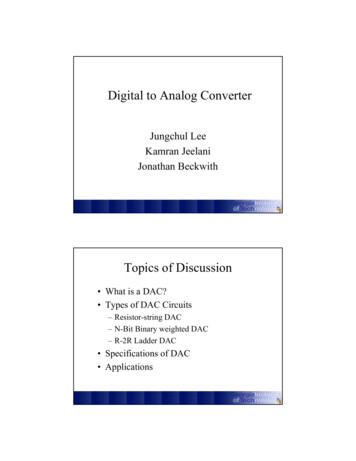
Digital to Analog ConverterJungchul LeeKamran JeelaniJonathan BeckwithTopics of Discussion What is a DAC? Types of DAC Circuits– Resistor-string DAC– N-Bit Binary weighted DAC– R-2R Ladder DAC Specifications of DAC Applications1
What is a DAC? Digital-to-Analog Converter: An electronic device, often anintegrated circuit, that converts a digital number into acorresponding analog voltage or current. Relation between analog signal and digital equivalentnVa bi 2 i Vrefi 1 AD conversion – Va - bi (encoder) ex) Transducer interface DA conversion – bi - Va (decoder) ex) motor, heater controlDAC configurations Assume the analog signal is a voltageDN-1, DN-2D1, D0 N-bit digital wordVRefAnalog voltage signal VOutDAC Vref*D/2NVOut2
Types of DAC Circuits1. Resistor-string2. N-Bit Binary Weighted Resistor3. R-2R LadderA Resistor-string DACV RefExample of 3 bit resistor-string DACR1RRequired component01- a resistor stringR01R- a set of switches – select output to use0- opamp – buffer1RVo01R0N 11RV0 VRef 01Ri 00B2B1bi2i 1B03
Resistor String DAC Example How many resistors and switches would be required toimplement an 8 bit resistor-string DAC?# of resistors 2N 28 256Ans)N 1i8# of switches 2 2 1 255i 0Impractical for converters with more than a few bits ofresolutionN-Bit Binary Weighted ResistorR/2121212122R4RN3I0124V outI0 VR i 12(bii 1)R8R LSBR52 1-MSB2 (N-1)RV0 -R f I0V Ref4
N-bit binary weighted Example Find output voltage, current, and resolutionfor a binary weighted resistor DAC of 4 bits- given conditionR 10 kΩ, Rf 5 kΩ, VR -10 VApplied binary word is 1001Example SolutionsRf R/25 kΩ3R-24Vout? 512 BitR21 Bit2R20 Bit4R228R10 kΩ3 Bit-10 V311331311 0 0 1 – binary inputVR5
Example Solutions (Cont.)Ans) 10 V 1001 0414243Ω 2 10 2 10 2 10 2 104 0.001125 AI0 V0 R f I0 (5 103 Ω) ( 0.001125A) 5.625VResolution LSB VRef 10V 4 0.625V2n2Example Solutions (Cont.)DN-1, DN-2 D1, D0 VRefVOutDAC Vref*D/2NVOut Binary Word input 10012 910 # of input combination : 24 16 Vout Vref * D/2N 10*9/16 5.625 V6
Limitations of the Binary Weighted DAC1. If R 10 kΩ, 8 bits DAC, and VRef 10 VR8 28-1*(10 kΩ) 1280 kΩI8 VRef/R8 10V/1280 kΩ 7.8 µAOp-amps that can handle those currents are rare and expensive.2. If R 10 Ω and VRef 10 VR1 21-1*(10 Ω) 10 ΩI1 VRef/R1 10V/10 Ω 1 AThis current is more than a typical op-amp can handle.R-2R Resistor Ladder DACVsRRR2R2R2R2R2RBit 3Bit 2Bit 1Bit 0RVout - Simplest type of DAC Requires only two precision resistance value (R and 2R)7
R-2R Resistor Ladder DACV3V2V1V0VsRR2RR2R2R2R2RBit 3Bit 2Bit 1Bit 0Each Bit controls a switch betweenground and the inverting input of theop ampThe switch is connected to ground ifthe corresponding bit 0RVout 4 Bit ConverterR-2R DAC ExampleEx. Convert 0001 to analogV3V2V1V0VsRR2RR2R2R2R2RBit 2Bit 1Bit 0Switch for bit 0 is connected toop amp input. All other switchesconnected to ground2RBit 32RR-OOO1 Digital Value:Vout8
R-2R DAC Example (cont.)V3VsV2V1V0RR2RR2R2R2R2RBit 3Bit 2Bit 1Bit 0Find EquivalentResistanceR-Vout Non-inverting input isconnected to ground.Therefore, inverting inputis at virtual groundR-2R DAC Example (cont.)V3V2RV1RV0V02RR2R2R2R2RBit 3Bit 2Bit 1Bit 02R2RRBit 0 -VsVoutReq 2R // 2R RApply voltage division:V0 V1 x Req(Req R)V0 ½ V19
R-2R DAC Example (cont.)V3VsV2V1RRV02RR2R2R2R2RBit 3Bit 2Bit 1Bit 0We have shown that V0 ½ V1Similarly, It can be proven that :R -VoutV1 ½ V2ANDV2 ½ V3Therefore:V0 1/8 V3 1/8 VsR-2R DAC Example (cont.)VsV3V2V1V0RRR2R2R2RBit3Bit 2 Bit 1 Bit 02R2RRVout -V0 is the input to the inverting amplifier circuit, which has a gain of:Av -R/2R -1/2Therefore, the analog output voltage corresponding to the binary input 0001 is:Vout0 Av (V0) (-1/2)(1/8*Vs)Vout0 -1/16 Vs10
R-2R DAC Example (cont.)We have shown that the analog output voltage for the digital input 0001 is:Vout0 -1/16 VsSimilarly, it can be show that:For input 0010:Vout1 -1/8 VsFor input 0100:Vout2 -1/4 VsFor input 1000:Vout3 -1/2 VsThe output for any combination of bits comprising the input binarynumber can now be found using the principle of superposition:Vout b3Vout3 b2Vout2 b1Vout1 b0Vout0General DAC CharacteristicsThere are six key parameters you should consider whenchoosing a DAC. Reference VoltageResolutionLinearitySpeedSettling TimeError11
Reference VoltageTo a large extent, the characteristics of a DAC are definedby its reference voltage. Non-multiplier DAC: Vref is fixed (specified by themanufacturer) Multiplier DAC: Vref is provided via an external sourceFull Scale VoltageDefined as the output when the digital input word is all1’s. 2N 1 V fs Vref N 2 12
ResolutionResolution is a measure of precision, not accuracy. It is defined asthe voltage change corresponding to changing the LSB. Many options in the 8-16 bit range, with 12 bits being a typicalcost / resolution trade off. More bitsMore stepsGreater ResolutionResolution VLSB VRef / 2N*where N is the number of bitsLinearityVoltage output Ideally, a DAC will produce a linear relationshipbetween a binary word and analog output00000011010201131004101511061117Digital Input Signal (3-bit)13
SpeedUsually specified as conversion or sampling rate. High speed DACs are typically defined as 1MS/s (1Mhz) Some current 12-16 bit DACs can reach the 1GHz range Conversion of input signal is limited by– Clock speed of the input signal– Settling time of the DACSettling Time Ideally, an instantaneous change in analog voltage would occurwhen a new binary word enters into a DAC. Settling time is the time taken by the DAC to reach ½ of the LSBof its new voltage. Components include delay, slew time, and ring time. Fast converters reduce slew time, but usually result in longer ringtimes. Delay time is normally a small term.14
Settling Time (cont.)Cause of Delay Time, Settling Time, and Ring TimeR-2R Resistor Ladder DACVsRRR2R2R2R2R2RBit 3Bit 2Bit 1Bit 0R -Delay time is caused bythe time it takes tochange these switchesbased on input bits.VoutSettling time and Ringtime is determined bythe op-amp’s slew rate15
Possible ErrorBecause we do not live in an “ideal” world, considerations forpossible error should be made. Non-Linearity– Integral– Differential Non Monotonicity Offset Error Gain ErrorIntegral Non-linearity Defined as the deviation of a DAC's transfer function from a straight line.The straight line can be a best approximation to the actual transfer function, or a linedrawn between the transfer function's end points (after subtracting the gain and offseterrors16
Differential Non-Linearity The difference between an actual step height and the ideal value of1LSB. Should be less than or equal to one to insure monotonicity.Non-Monotonicity A monotonic DAC yields an increase in output as input increases. If a differential non-linearity of greater than 1LSB occurs, increasingthe digital input may actually result in a decreased output.76Analog 611071118Digital Input17
Gain Error Defined as the difference between the ideal max output voltage and the actual max outputvoltage (after subtracting offset error). Changes the slope of the output, thereby creating the same percentage error for each step. Expressed in mV as a percentage of the maximum output.Offset Error The offset error equals the analog output when the digital signal is zero. Typically defined in absolute millivolts with (10mV being acceptable).18
Cause of Non-Linearity, Gain error, and Offset errorR-2R Resistor Ladder DACNon-linearity is caused bythe resistors. Resistors inD/A converters need to bematched but manufacturingexact resistors is difficult.RRR2R2R2R2R2RBit 3Bit 2Bit 1Bit 0R -VsVoutGain Error and OffsetError is caused by op-ampand or op-amp’s feedbackresistorDAC Applications DAC’s can be found in any device that interfaces digital and analog circuitry Analog Displays Digital Control Systems Digital Audio Communications Countless other applications19
References Digital-Analog Converters Are a "Bit" Analog – Maxim m/appnote number/1055/ln/en) Component and Measurement Advances Ensure 16-Bit DAC Settling Time– Jim Williams, Linear Technology July 1998 Introduction to Mechatronics and Measurement systems – David G.Alciatore and Michael B. Histand, McGrawHill Mechatronics-Electronic control systems in mechanical and electricalengineering-W. Bolton, Longman Introduction to Electronic Circuit Design-Richard R. Spencer andMohammed S. Ghausi, PrenticeHallQuestions ?20
integrated circuit, that converts a digital number into a corresponding analog voltage or current. Relation between analog signal and digital equivalent n a i re i f i1 V b 2 V AD conversion – Va- bi (encoder) ex) Transducer interface DA conversion – bi-