Transcription
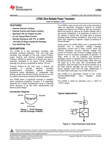
LP395www.ti.comSNOSBF3C – APRIL 1998 – REVISED MARCH 2013LP395 Ultra Reliable Power TransistorCheck for Samples: LP395FEATURES1 2Internal Thermal LimitingInternal Current and Power LimitingSpecified 100 mA Output Current0.5 μA Typical Base CurrentDirectly Interfaces with TTL or CMOS 36 Volts On Base Causes No Damage2 μs Switching TimeDESCRIPTIONThe LP395 is a fast monolithic transistor withcomplete overload protection. This very high gaintransistor has included on the chip, current limiting,power limiting, and thermal overload protection,making it difficult to destroy from almost any type ofoverload. Available in an epoxy TO-92 transistorpackage this device is specified to deliver 100 mA.Thermal limiting at the chip level, a feature eprotectionagainstoverload.Excessive power dissipation or inadequate heatsinking causes the thermal limiting circuitry to turn offthe device preventing excessive die temperature.The LP395 offers a significant increase in reliabilitywhile simplifying protection circuitry. It is especiallyattractive as a small incandescent lamp or solenoiddriver because of its low drive requirements andblowout-proof design.Connection DiagramThe LP395 is easy to use and only a few precautionsneed be observed. Excessive collector to emittervoltage can destroy the LP395 as with any transistor.When the device is used as an emitter follower with alow source impedance, it is necessary to insert a 4.7kΩ resistor in series with the base lead to preventpossible emitter follower oscillations. Also since it hasgood high frequency response, supply by-passing isrecommended.Areas where the LP395 differs from a standard NPNtransistor are in saturation voltage, leakage(quiescent) current and in base current. Since theinternal protection circuitry requires voltage andcurrent to function, the minimum voltage across thedevice in the on condition (saturated) is typically 1.6Volts, while in the off condition the quiescent(leakage) current is typically 200 μA. Base current inthis device flows out of the base lead, rather than intothe base as is the case with conventional NPNtransistors. Also the base can be driven positive up to36 Volts without damage, but will draw current ifdriven negative more than 0.6 Volts. Additionally, ifthe base lead is left open, the LP395 will turn on.The LP395 is a low-power version of the .The LP395 is rated for operation over a 40 C to 125 C range.Typical ApplicationsFigure 1. TO-92 PackageSee NS Package LP0003AFigure 2. Fully Protected Lamp Driver12Please be aware that an important notice concerning availability, standard warranty, and use in critical applications ofTexas Instruments semiconductor products and disclaimers thereto appears at the end of this data sheet.All trademarks are the property of their respective owners.PRODUCTION DATA information is current as of publication date.Products conform to specifications per the terms of the TexasInstruments standard warranty. Production processing does notnecessarily include testing of all parameters.Copyright 1998–2013, Texas Instruments Incorporated
LP395SNOSBF3C – APRIL 1998 – REVISED MARCH 2013www.ti.comThese devices have limited built-in ESD protection. The leads should be shorted together or the device placed in conductive foamduring storage or handling to prevent electrostatic damage to the MOS gates.ABSOLUTE MAXIMUM RATINGS (1)Collector to Emitter Voltage36VCollector to Base Voltage36VBase to Emitter Voltage (Forward)36VBase to Emitter Voltage (Reverse)10VBase to Emitter Current (Reverse)20 mACollector Current LimitInternally LimitedPower DissipationInternally LimitedOperating Temperature Range 40 C to 125 CStorage Temperature Range 65 C to 150 CLead Temp. (Soldering, 10 seconds)(1)260 CAbsolute Maximum Ratings indicate limits beyond which damage to the device may occur. Operating Ratings indicate conditions forwhich the device is functional, but do not ensure specific performance limits.ELECTRICAL CHARACTERISTICSSymbolVCEParameterCollector to EmitterConditionsTypical0.5 mA IC 100 mATested Limit Design Limit(1)(2)Units(Limit)3636V(Max)(3)Operating VoltageICLCollector Current Limit(4)VBE 2V, VCE 36V452520mA(Min)VBE 2V, VCE 15V906050mA(Min)mA(Min)VBE 2V, 2V VCE 6V130100100IBBase Current0 IC 100 mA 0.3 2.0 2.5μA(Max)IQQuiescent CurrentVBE 0V, 0 VCE 36V0.240.500.60mA(Max)VCE(SAT)Saturation VoltageVBE 2V, IC 100 mA1.822.002.10V(Max)BVBEBase to Emitter Break-0 VCE 36V, IB 2 μA3636V(Min)0.790.90V(Max)1.40V (Max)down VoltageVBE(4)Base to Emitter Voltage(5)tSSwitching TimeIC 5 mAIC 100 mA0.69(4)VCE 20V, RL 200Ω1.02μs2VBE 0V, 2V, 0VθJAThermal Resistance0.4″ leads soldered toJunction to Ambientprinted circuit board0.125″ leads soldered toprinted circuit board(1)(2)(3)(4)(5)2150180 C/W(Max)130160 C/W(Max)Specified and 100% production tested.Specified (but not 100% production tested) over the operating temperature and supply voltage ranges. These limits are not used tocalculate outgoing quality levels.Parameters identified with boldface type apply at temp. extremes. All other numbers, unless noted apply at 25 C.These numbers apply for pulse testing with a low duty cycle.Base positive with respect to emitter.Submit Documentation FeedbackCopyright 1998–2013, Texas Instruments IncorporatedProduct Folder Links: LP395
LP395www.ti.comSNOSBF3C – APRIL 1998 – REVISED MARCH 2013SIMPLIFIED CIRCUITAPPLICATIONS INFORMATIONOne failure mode incandescent lamps may experience is one in which the filament resistance drops to a very lowvalue before it actually blows out. This is especially rough on most solid-state lamp drivers and in most cases alamp failure of this type will also cause the lamp driver to fail. Because of its high gain and blowout-proof design,the LP395 is an ideal candidate for reliably driving small incandescent lamps. Additionally, the current limitingcharacteristics of the LP395 are advantageous as it serves to limit the cold filament inrush current, thusincreasing lamp life.Submit Documentation FeedbackCopyright 1998–2013, Texas Instruments IncorporatedProduct Folder Links: LP3953
LP395SNOSBF3C – APRIL 1998 – REVISED MARCH 2013www.ti.comTYPICAL PERFORMANCE CHARACTERISTICS45 Volt Transfer Function36 Volt Transfer FunctionFigure 3.Figure 4.Collector CharacteristicsAvailable Collector CurrentFigure 5.Figure 6.Quiescent Collector CurrentSaturation VoltageFigure 7.Figure 8.Submit Documentation FeedbackCopyright 1998–2013, Texas Instruments IncorporatedProduct Folder Links: LP395
LP395www.ti.comSNOSBF3C – APRIL 1998 – REVISED MARCH 2013TYPICAL PERFORMANCE CHARACTERISTICS (continued)Collector Current ThresholdFigure 9.Submit Documentation FeedbackCopyright 1998–2013, Texas Instruments IncorporatedProduct Folder Links: LP3955
LP395SNOSBF3C – APRIL 1998 – REVISED MARCH 2013www.ti.comTYPICAL APPLICATIONSFigure 10. Lamp Flasher(Short Circuit Proof)Figure 11. Optically IsolatedSwitchFigure 12. Two TerminalCurrent LimiterFigure 13. Composite PNP6Submit Documentation FeedbackCopyright 1998–2013, Texas Instruments IncorporatedProduct Folder Links: LP395
LP395www.ti.comSNOSBF3C – APRIL 1998 – REVISED MARCH 2013REVISION HISTORYChanges from Revision B (March 2013) to Revision C PageChanged layout of National Data Sheet to TI format . 6Submit Documentation FeedbackCopyright 1998–2013, Texas Instruments IncorporatedProduct Folder Links: LP3957
PACKAGE OPTION ADDENDUMwww.ti.com6-Jul-2014PACKAGING INFORMATIONOrderable DeviceStatus(1)Package Type Package Pins PackageDrawingQtyEco PlanLead/Ball FinishMSL Peak Temp(2)(6)(3)Op Temp ( C)Device Marking(4/5)LP395Z/LFT1ACTIVETO-92LP32000Green (RoHS& no Sb/Br)CU SNN / A for Pkg TypeLP395ZLP395Z/LFT4ACTIVETO-92LP32000Green (RoHS& no Sb/Br)CU SNN / A for Pkg TypeLP395ZLP395Z/NOPBACTIVETO-92LP31800Green (RoHS& no Sb/Br)CU SNN / A for Pkg Type-40 to 125LP395Z(1)The marketing status values are defined as follows:ACTIVE: Product device recommended for new designs.LIFEBUY: TI has announced that the device will be discontinued, and a lifetime-buy period is in effect.NRND: Not recommended for new designs. Device is in production to support existing customers, but TI does not recommend using this part in a new design.PREVIEW: Device has been announced but is not in production. Samples may or may not be available.OBSOLETE: TI has discontinued the production of the device.(2)Eco Plan - The planned eco-friendly classification: Pb-Free (RoHS), Pb-Free (RoHS Exempt), or Green (RoHS & no Sb/Br) - please check http://www.ti.com/productcontent for the latest availabilityinformation and additional product content details.TBD: The Pb-Free/Green conversion plan has not been defined.Pb-Free (RoHS): TI's terms "Lead-Free" or "Pb-Free" mean semiconductor products that are compatible with the current RoHS requirements for all 6 substances, including the requirement thatlead not exceed 0.1% by weight in homogeneous materials. Where designed to be soldered at high temperatures, TI Pb-Free products are suitable for use in specified lead-free processes.Pb-Free (RoHS Exempt): This component has a RoHS exemption for either 1) lead-based flip-chip solder bumps used between the die and package, or 2) lead-based die adhesive used betweenthe die and leadframe. The component is otherwise considered Pb-Free (RoHS compatible) as defined above.Green (RoHS & no Sb/Br): TI defines "Green" to mean Pb-Free (RoHS compatible), and free of Bromine (Br) and Antimony (Sb) based flame retardants (Br or Sb do not exceed 0.1% by weightin homogeneous material)(3)MSL, Peak Temp. - The Moisture Sensitivity Level rating according to the JEDEC industry standard classifications, and peak solder temperature.(4)There may be additional marking, which relates to the logo, the lot trace code information, or the environmental category on the device.(5)Multiple Device Markings will be inside parentheses. Only one Device Marking contained in parentheses and separated by a " " will appear on a device. If a line is indented then it is a continuationof the previous line and the two combined represent the entire Device Marking for that device.(6)Lead/Ball Finish - Orderable Devices may have multiple material finish options. Finish options are separated by a vertical ruled line. Lead/Ball Finish values may wrap to two lines if the finishvalue exceeds the maximum column width.Important Information and Disclaimer:The information provided on this page represents TI's knowledge and belief as of the date that it is provided. TI bases its knowledge and belief on informationprovided by third parties, and makes no representation or warranty as to the accuracy of such information. Efforts are underway to better integrate information from third parties. TI has taken andAddendum-Page 1Samples
PACKAGE OPTION ADDENDUMwww.ti.com6-Jul-2014continues to take reasonable steps to provide representative and accurate information but may not have conducted destructive testing or chemical analysis on incoming materials and chemicals.TI and TI suppliers consider certain information to be proprietary, and thus CAS numbers and other limited information may not be available for release.In no event shall TI's liability arising out of such information exceed the total purchase price of the TI part(s) at issue in this document sold by TI to Customer on an annual basis.Addendum-Page 2
IMPORTANT NOTICETexas Instruments Incorporated and its subsidiaries (TI) reserve the right to make corrections, enhancements, improvements and otherchanges to its semiconductor products and services per JESD46, latest issue, and to discontinue any product or service per JESD48, latestissue. Buyers should obtain the latest relevant information before placing orders and should verify that such information is current andcomplete. All semiconductor products (also referred to herein as “components”) are sold subject to TI’s terms and conditions of salesupplied at the time of order acknowledgment.TI warrants performance of its components to the specifications applicable at the time of sale, in accordance with the warranty in TI’s termsand conditions of sale of semiconductor products. Testing and other quality control techniques are used to the extent TI deems necessaryto support this warranty. Except where mandated by applicable law, testing of all parameters of each component is not necessarilyperformed.TI assumes no liability for applications assistance or the design of Buyers’ products. Buyers are responsible for their products andapplications using TI components. To minimize the risks associated with Buyers’ products and applications, Buyers should provideadequate design and operating safeguards.TI does not warrant or represent that any license, either express or implied, is granted under any patent right, copyright, mask work right, orother intellectual property right relating to any combination, machine, or process in which TI components or services are used. Informationpublished by TI regarding third-party products or services does not constitute a license to use such products or services or a warranty orendorsement thereof. Use of such information may require a license from a third party under the patents or other intellectual property of thethird party, or a license from TI under the patents or other intellectual property of TI.Reproduction of significant portions of TI information in TI data books or data sheets is permissible only if reproduction is without alterationand is accompanied by all associated warranties, conditions, limitations, and notices. TI is not responsible or liable for such altereddocumentation. Information of third parties may be subject to additional restrictions.Resale of TI components or services with statements different from or beyond the parameters stated by TI for that component or servicevoids all express and any implied warranties for the associated TI component or service and is an unfair and deceptive business practice.TI is not responsible or liable for any such statements.Buyer acknowledges and agrees that it is solely responsible for compliance with all legal, regulatory and safety-related requirementsconcerning its products, and any use of TI components in its applications, notwithstanding any applications-related information or supportthat may be provided by TI. Buyer represents and agrees that it has all the necessary expertise to create and implement safeguards whichanticipate dangerous consequences of failures, monitor failures and their consequences, lessen the likelihood of failures that might causeharm and take appropriate remedial actions. Buyer will fully indemnify TI and its representatives against any damages arising out of the useof any TI components in safety-critical applications.In some cases, TI components may be promoted specifically to facilitate safety-related applications. With such components, TI’s goal is tohelp enable customers to design and create their own end-product solutions that meet applicable functional safety standards andrequirements. Nonetheless, such components are subject to these terms.No TI components are authorized for use in FDA Class III (or similar life-critical medical equipment) unless authorized officers of the partieshave executed a special agreement specifically governing such use.Only those TI components which TI has specifically designated as military grade or “enhanced plastic” are designed and intended for use inmilitary/aerospace applications or environments. Buyer acknowledges and agrees that any military or aerospace use of TI componentswhich have not been so designated is solely at the Buyer's risk, and that Buyer is solely responsible for compliance with all legal andregulatory requirements in connection with such use.TI has specifically designated certain components as meeting ISO/TS16949 requirements, mainly for automotive use. In any case of use ofnon-designated products, TI will not be responsible for any failure to meet dioAutomotive and fier.ti.comCommunications and Telecomwww.ti.com/communicationsData Convertersdataconverter.ti.comComputers and Peripheralswww.ti.com/computersDLP Productswww.dlp.comConsumer ergy and Lightingwww.ti.com/energyClocks and wer Mgmtpower.ti.comSpace, Avionics and ollersmicrocontroller.ti.comVideo and Imagingwww.ti.com/videoRFIDwww.ti-rfid.comOMAP Applications Processorswww.ti.com/omapTI E2E Communitye2e.ti.comWireless Connectivitywww.ti.com/wirelessconnectivityMailing Address: Texas Instruments, Post Office Box 655303, Dallas, Texas 75265Copyright 2014, Texas Instruments Incorporated
The LP395 is a fast monolithic transistor with internal protection circuitry requires voltage and complete overload protection. This very high gain current to function, the minimum voltage across the transistor has included on the chip, current limiting, device in the on condition (saturated) is typically 1.6