Transcription
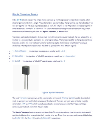
Bipolar Transistor BasicsIn the Diode tutorials we saw that simple diodes are made up from two pieces of semiconductor material, eithersilicon or germanium to form a simple PN-junction and we also learnt about their properties and characteristics. If wenow join together two individual signal diodes back-to-back, this will give us two PN-junctions connected together inseries that share a common P or N terminal. The fusion of these two diodes produces a three layer, two junction,three terminal device forming the basis of a Bipolar Transistor, or BJT for short.Transistors are three terminal active devices made from different semiconductor materials that can act as either aninsulator or a conductor by the application of a small signal voltage. The transistor's ability to change between thesetwo states enables it to have two basic functions: "switching" (digital electronics) or "amplification" (analogueelectronics). Then bipolar transistors have the ability to operate within three different regions: 1. Active Region - the transistor operates as an amplifier and Ic β.Ib 2. Saturation - the transistor is "fully-ON" operating as a switch and Ic I(saturation) 3. Cut-off - the transistor is "fully-OFF" operating as a switch and Ic 0Typical Bipolar TransistorThe word Transistor is an acronym, and is a combination of the words Transfer Varistor used to describe theirmode of operation way back in their early days of development. There are two basic types of bipolar transistorconstruction, NPN and PNP, which basically describes the physical arrangement of the P-type and N-typesemiconductor materials from which they are made.The Bipolar Transistor basic construction consists of two PN-junctions producing three connecting terminals witheach terminal being given a name to identify it from the other two. These three terminals are known and labelled asthe Emitter ( E ), the Base ( B ) and the Collector ( C ) respectively.
Bipolar Transistors are current regulating devices that control the amount of current flowing through them inproportion to the amount of biasing voltage applied to their base terminal acting like a current-controlled switch. Theprinciple of operation of the two transistor types NPN and PNP, is exactly the same the only difference being in theirbiasing and the polarity of the power supply for each type.Bipolar Transistor ConstructionThe construction and circuit symbols for both the NPN and PNP bipolar transistor are given above with the arrow inthe circuit symbol always showing the direction of "conventional current flow" between the base terminal and itsemitter terminal. The direction of the arrow always points from the positive P-type region to the negative N-typeregion for both transistor types, exactly the same as for the standard diode symbol.Bipolar Transistor Configurations
As the Bipolar Transistor is a three terminal device, there are basically three possible ways to connect it within anelectronic circuit with one terminal being common to both the input and output. Each method of connectionresponding differently to its input signal within a circuit as the static characteristics of the transistor vary with eachcircuit arrangement. 1. Common Base Configuration - has Voltage Gain but no Current Gain. 2. Common Emitter Configuration - has both Current and Voltage Gain. 3. Common Collector Configuration - has Current Gain but no Voltage Gain.The Common Base (CB) ConfigurationAs its name suggests, in the Common Base or grounded base configuration, the BASE connection is common toboth the input signal AND the output signal with the input signal being applied between the base and the emitterterminals. The corresponding output signal is taken from between the base and the collector terminals as shown withthe base terminal grounded or connected to a fixed reference voltage point. The input current flowing into the emitteris quite large as its the sum of both the base current and collector current respectively therefore, the collector currentoutput is less than the emitter current input resulting in a current gain for this type of circuit of "1" (unity) or less, inother words the common base configuration "attenuates" the input signal.The Common Base Transistor CircuitThis type of amplifier configuration is a non-inverting voltage amplifier circuit, in that the signal voltages Vin and Voutare in-phase. This type of transistor arrangement is not very common due to its unusually high voltage gaincharacteristics. Its output characteristics represent that of a forward biased diode while the input characteristicsrepresent that of an illuminated photo-diode. Also this type of bipolar transistor configuration has a high ratio of outputto input resistance or more importantly "load" resistance (RL) to "input" resistance (Rin) giving it a value of"Resistance Gain". Then the voltage gain (Av for a common base configuration is therefore given as:Common Base Voltage Gain
The common base circuit is generally only used in single stage amplifier circuits such as microphone pre-amplifier orradio frequency (Rf) amplifiers due to its very good high frequency response.The Common Emitter (CE) ConfigurationIn the Common Emitter or grounded emitter configuration, the input signal is applied between the base, while theoutput is taken from between the collector and the emitter as shown. This type of configuration is the most commonlyused circuit for transistor based amplifiers and which represents the "normal" method of bipolar transistor connection.The common emitter amplifier configuration produces the highest current and power gain of all the three bipolartransistor configurations. This is mainly because the input impedance is LOW as it is connected to a forward-biasedPN-junction, while the output impedance is HIGH as it is taken from a reverse-biased PN-junction.The Common Emitter Amplifier CircuitIn this type of configuration, the current flowing out of the transistor must be equal to the currents flowing into thetransistor as the emitter current is given as Ie Ic Ib. Also, as the load resistance (RL) is connected in series withthe collector, the current gain of the common emitter transistor configuration is quite large as it is the ratio of Ic/Ib andis given the Greek symbol of Beta, (β). As the emitter current for a common emitter configuration is defined asIe Ic Ib, the ratio of Ic/Ie is called Alpha, given the Greek symbol of α. Note: that the value of Alpha will alwaysbe less than unity.Since the electrical relationship between these three currents, Ib, Ic and Ie is determined by the physical constructionof the transistor itself, any small change in the base current (Ib), will result in a much larger change in the collector
current (Ic). Then, small changes in current flowing in the base will thus control the current in the emitter-collectorcircuit. Typically, Beta has a value between 20 and 200 for most general purpose transistors.By combining the expressions for both Alpha, α and Beta, β the mathematical relationship between theseparameters and therefore the current gain of the transistor can be given as:Where: "Ic" is the current flowing into the collector terminal, "Ib" is the current flowing into the base terminal and "Ie"is the current flowing out of the emitter terminal.Then to summarise, this type of bipolar transistor configuration has a greater input impedance, current and powergain than that of the common base configuration but its voltage gain is much lower. The common emitteroconfiguration is an inverting amplifier circuit resulting in the output signal being 180 out-of-phase with the inputvoltage signal.The Common Collector (CC) ConfigurationIn the Common Collector or grounded collector configuration, the collector is now common through the supply. Theinput signal is connected directly to the base, while the output is taken from the emitter load as shown. This type ofconfiguration is commonly known as a Voltage Follower or Emitter Follower circuit. The emitter followerconfiguration is very useful for impedance matching applications because of the very high input impedance, in theregion of hundreds of thousands of Ohms while having a relatively low output impedance.The Common Collector Transistor Circuit
The common emitter configuration has a current gain approximately equal to the β value of the transistor itself. In thecommon collector configuration the load resistance is situated in series with the emitter so its current is equal to thatof the emitter current. As the emitter current is the combination of the collector AND the base current combined, theload resistance in this type of transistor configuration also has both the collector current and the input current of thebase flowing through it. Then the current gain of the circuit is given as:The Common Collector Current GainThis type of bipolar transistor configuration is a non-inverting circuit in that the signal voltages of Vin and Vout are inphase. It has a voltage gain that is always less than "1" (unity). The load resistance of the common collector transistorreceives both the base and collector currents giving a large current gain (as with the common emitter configuration)therefore, providing good current amplification with very little voltage gain.
Bipolar Transistor SummaryThen to summarise, the behaviour of the bipolar transistor in each one of the above circuit configurations is verydifferent and produces different circuit characteristics with regards to input impedance, output impedance and gainwhether this is voltage gain, current gain or power gain and this is summarised in the table below.Bipolar Transistor CharacteristicsThe static characteristics for a Bipolar Transistor can be divided into the following three main groups.Input Characteristics:-Common Base Common Emitter -ΔVEB / ΔIEΔVBE / ΔIBOutput Characteristics:-Common Base Common Emitter -ΔVC / ΔICΔVC / ΔICTransfer Characteristics:- Common Base Common Emitter -ΔIC / ΔIEΔIC / ΔIBwith the characteristics of the different transistor configurations given in the following ollectorInput ImpedanceLowMediumHighOutput ImpedanceVery HighHighLowoooPhase Angle01800Voltage GainHighMediumLowCurrent GainLowMediumHighPower GainLowVery HighMediumIn the next tutorial about Bipolar Transistors, we will look at the NPN Transistor in more detail when used in thecommon emitter configuration as an amplifier as this is the most widely used configuration due to its flexibility andhigh gain. We will also plot the output characteristics curves commonly associated with amplifier circuits as a functionof the collector current to the base current.The NPN Transistor
In the previous tutorial we saw that the standard Bipolar Transistor or BJT, comes in two basic forms. An NPN(Negative-Positive-Negative) type and a PNP (Positive-Negative-Positive) type, with the most commonly usedtransistor type being the NPN Transistor. We also learnt that the transistor junctions can be biased in one of threedifferent ways - Common Base, Common Emitter and Common Collector. In this tutorial we will look more closelyat the "Common Emitter" configuration using NPN Transistors with an example of the construction of a NPNtransistor along with the transistors current flow characteristics is given below.An NPN Transistor ConfigurationNote: Conventional current flow.We know that the transistor is a "current" operated device (Beta model) and that a large current ( Ic ) flows freelythrough the device between the collector and the emitter terminals when the transistor is switched "fully-ON".However, this only happens when a small biasing current ( Ib ) is flowing into the base terminal of the transistor at thesame time thus allowing the Base to act as a sort of current control input. The transistor current in an NPN transistoris the ratio of these two currents ( Ic/Ib ), called the DC Current Gain of the device and is given the symbol of hfe ornowadays Beta, ( β ). The value of β can be large up to 200 for standard transistors, and it is this large ratio betweenIc and Ib that makes the NPN transistor a useful amplifying device when used in its active region as Ib provides theinput and Ic provides the output. Note that Beta has no units as it is a ratio.Also, the current gain of the transistor from the Collector terminal to the Emitter terminal, Ic/Ie, is called Alpha, ( α ),and is a function of the transistor itself (electrons diffusing across the junction). As the emitter current Ie is theproduct of a very small base current plus a very large collector current, the value of alpha α, is very close to unity,and for a typical low-power signal transistor this value ranges from about 0.950 to 0.999α and β Relationship in a NPN Transistor
By combining the two parameters α and β we can produce two mathematical expressions that gives the relationshipbetween the different currents flowing in the transistor.The values of Beta vary from about 20 for high current power transistors to well over 1000 for high frequency lowpower type bipolar transistors. The value of Beta for most standard NPN transistors can be found in themanufactures datasheets but generally range between 50 - 200.The equation above for Beta can also be re-arranged to make Ic as the subject, and with a zero base current ( Ib 0 ) the resultant collector current Ic will also be zero, ( β x 0 ). Also when the base current is high the corresponding
collector current will also be high resulting in the base current controlling the collector current. One of the mostimportant properties of the Bipolar Junction Transistor is that a small base current can control a much largercollector current. Consider the following example.Example No1An NPN Transistor has a DC current gain, (Beta) value of 200. Calculate the base current Ib required to switch aresistive load of 4mA.Therefore, β 200, Ic 4mA and Ib 20µA.One o
The transistor's ability to change between these two states enables it to have two basic functions: "switching" (digital electronics) or "amplification" (analogue electronics). Then bipolar transistors have the ability to operate within three different regions: 1. Active Region - the transistor operates as an amplifier and . Ic β.Ib 2. Saturation -the transistor is "fully ON" operating as a switch and