Transcription
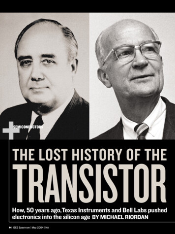
TRANSISTORSEMICONDUCTORSTHE LOST HISTORY OF THEHow, 50 years ago,Texas Instruments and Bell Labs pushedelectronics into the silicon age BY MICHAEL RIORDAN44 IEEE Spectrum May 2004 NA
he speaker’s words were at once laconic and electrifying.“Contrary to what my colleagues have told you about thebleak prospects for silicon transistors,” he proclaimed inhis matter-of-fact voice, “I happen to have a few of them herein my pocket.”Silicon transistors? Did he say silicon transistors?Yes—among the few in the world at that moment. It was10 May 1954.A long and till-then uneventful session on silicon devices hadbeen winding down at the Institute of Radio Engineers (IRE)National Conference on Airborne Electronics, in Dayton, Ohio.There, a parade of engineers and scientists were lamenting thesobering challenges of developing and eventually manufacturing silicon transistors. Amid the torpor, scattered attendees werestifling yawns, glancing at watches, and nodding off. But that wasbefore Gordon Teal of Texas Instruments Inc. made his surprising announcement—and jaws dropped in disbelief.“Did you say you have silicon transistors in production?”asked a stupefied listener about 10 rows back in the audience,which now began to perk up noticeably.“Yes, we have three types of silicon transistors in production,”TTeal replied, pulling several out of his pocket to the general amazement and envy of the crowd. Then, in a bit of quaint but effective razzle-dazzle, he cranked up a record player, which beganblaring out the swinging sounds of Artie Shaw’s big-band hit,“Summit Ridge Drive.” Amplified by germanium transistors, themusic died out instantly as Teal dunked one into a beaker ofhot oil. But when he repeated his demonstration immersing a silicon transistor instead, the music played on without faltering.As his talk ended, Teal mentioned that copies of his paper onthe subject, innocuously titled “Some Recent Developments inSilicon and Germanium Materials and Devices,” were availablenear the rear door. A crowd stampeded back to get them, leavingthe final speaker of the session without an audience. Minutes later,a Raytheon engineer was overheard in the lobby shouting into atelephone: “They’ve got the silicon transistor down in Texas!”IN THE BEGINNING: Gordon Teal [left] directed the development of the silicon transistor atTexas Instruments. William Shockley [middle] led the team at Bell Telephone Laboratories thatdeveloped the very first transistor, which was made of germanium. TI’s silicon device with itsthree long leads became famous, making the Texas upstart the sole supplier of silicon transistorsfor several years in the 1950s. Morris Tanenbaum [right] at Bell Labs actually made the firstsilicon transistor, but he felt “it didn’t look attractive” from a manufacturing point of view.May 2004 IEEE Spectrum NA 45
At the time, the silicon transistor seemed to be one of the firstmajor breakthroughs in transistor development not to occur at BellTelephone Laboratories in Murray Hill, N.J., where physicists JohnBardeen and Walter Brattain had invented the transistor in December1947. Their device featured two closely spaced metal points jabbeddelicately into a germanium surface—hence its name, the “pointcontact” transistor. They called one point the “emitter” and the otherpoint the “collector,” while a third contact, known as the “base,”was applied to the back side of the germanium sliver. A positive electrical bias on the emitter enhanced the conductivity of the germanium just beneath the collector point, amplifying the output currentthat flowed to it from the base.Bell Labs achieved a long string of firstsin the years following that momentousinvention, which it announced six monthslater at a 30 June 1948 press conference inNew York City. Among its major advanceswas the so-called junction transistor, firstconceived the previous January by WilliamShockley, who led the group that includedBardeen and Brattain. He figured that muchbetter transistor performance and reliability could be realized by eliminating the fragile point contacts and instead forming theemitter, base, and collector as a single semiconductor sandwich with three different layers [see sidebar,“Transistors 101: The Junction Transistor”]. Current flowing fromemitter to collector in Shockley’s device could be modulated by aninput signal on the base.Teal (then working at Bell Labs) and his fellow physical chemistMorgan Sparks successfully fabricated the first working junction transistor from a germanium crystal in April 1950. But—partlybecause the frequency response of early junction transistors wasinferior to that of point-contact devices—Bell Labs held offannouncing this achievement for over a year, until 4 July 1951. Fiveyears later, Bardeen, Brattain, and Shockley shared the Nobel Prizefor inventing this revolutionary solid-state amplifier.Their brilliant pioneering work has overshadowed much of thesubsequent development years of the transistor, including thecrucial change from germanium to silicon in the mid-1950s. Thatshift in semiconductor material proved essential to the device’sglorious future as the fundamental building block of virtually allof today’s integrated circuits. For germanium, to put it simply, wasjust not up to the task.The material does have advantages: it is far less reactive thansilicon and much easier to work with because of its lower meltingtemperature. And current carriers—electrons and holes—flow throughgermanium more rapidly than through silicon, which leads to higherfrequency response. But germanium also has serious limitations. Forexample, it has a low band gap (0.67 electron volts versus 1.12 eV forsilicon), the energy required to knock electrons out of atoms into theconduction band. So transistors made of this silvery element havemuch higher leakage currents: as the temperature increases, their delicately balanced junctions become literally drowned in a swarmingsea of free electrons. Above about 75 C, germanium transistors quitworking altogether. These limitations proved bothersome to radiomanufacturers and especially the armed services, which needed stable, reliable equipment that would perform in extreme conditions.Nowhere were these concerns appreciated more than at Bell Labs,which led the way into silicon semiconductor research during theearly 1950s. Working in its chemical physics department with technician Ernie Buehler, Teal grew single crystals of silicon and “doped”them with tiny impurities to make solid-state diodes inFebruary 1951, publishing the results a year later. He added specificimpurity atoms to the molten silicon to alter the electrical properties of crystals drawn from it. Elements from the fifth columnof the periodic table—arsenic or antimony, for example—create anexcess of electrons in the tetrahedral crystal structure, yieldingn-type silicon. Elements from the third column, such as boron orgallium, create a deficit of electrons (usually regarded as an excessof holes), yielding p-type silicon. By adding first one kind of impurity and then the other to the molten silicon from which they slowlywithdrew the crystal, Teal and Buehler formed transition regionscalled pn junctions between the two types of silicon. Small bars cutacross these junctions act as diodes whena potential is applied across them throughelectrical contacts on the two ends.Meanwhile, Calvin Fuller was beginningexperiments in an adjacent lab on diffusing impurity atoms from hot gases into thegermanium or silicon surface—one of themajor technology milestones on the road tothe integrated circuit. By December 1953Fuller was so successful that Shockleystarted building a new research team toattempt to fabricate silicon transistors usingthe technique. And early in 1954, Fuller andGerald Pearson formed pn junctions by diffusing a thin layer of boron atoms into a wafer of n-type silicon, making a hole-rich p-layer on its surface. These large-area diodes generated substantial current when sunlight fell on them. On 25 April,Bell Labs trumpeted this achievement as the “solar battery,” thefirst photovoltaic cell operating at efficiencies near 10 percent.“They’ve gotthe silicontransistordown in Texas!”46 IEEE Spectrum May 2004 NABy then TI had made its first silicon transistor—under Teal’sgeneral direction. Back at Bell Labs, he had become homesick for hisnative Texas, where he had grown up a devout Baptist in South Dallasand pursued his undergraduate studies in mathematics and chemistry at Baylor University, in Waco. Restless in Murray Hill, N.J., andlooking for more responsibility, Teal responded to an ad in TheNew York Times for a research director at TI. He met with TI vicepresident Pat Haggerty, who offered him the position. He began thereon 1 January 1953, bringing with him his vast expertise in growingand doping semiconductor crystals.Under Haggerty’s leadership, TI was moving aggressively intomilitary electronics, then burgeoning with the Cold War in fullswing. The Dallas company had been founded during the 1930s asGeophysical Services Inc., developing and producing reflectionseismographs for the oil industry. During World War II, it snaggeda U.S. Navy contract to supply airborne submarine-detectionequipment; afterward it continued to expand its activities in military electronics, reorganizing itself as Texas Instruments Inc. in1951. By the time Teal arrived, the firm had almost 1800 employees and was generating about US 25 million in annual sales.The company was also beginning to manufacture what were calledgrown-junction germanium transistors under the direction of engineer Mark Shepherd. He had attended a 1951 Bell Labs symposium ontransistor technology with Haggerty, where he listened to a Teal workshop on growing semiconductor crystals. In early 1952, after muchwheedling and cajoling by Haggerty, TI purchased a patent licenseto produce transistors from Western Electric Co., AT&T’s manufacturing arm, for 25 000. By the end of that year, it was already manufacturing and selling them under Shepherd’s leadership.Early the next year, Teal was back in Dallas organizing TI’sPREVIOUS SPREAD: TEXAS INSTRUMENTS (TEAL, SHEPHERD, AND TRANSISTOR); MORRIS TANENBAUM
TRANSISTORS 101: THE JUNCTION TRANSISTORJOHN MACNEILLTo understand how a transistor works, first consider the lowlydiode. It is a simple union of the two most fundamental kinds ofsemiconductor, known as n-type and p-type. Both conductcurrent, but the n-type does it with electrons, while the p-typedepends on electron deficiencies, better known as holes.Joining these two types of semiconductors forms what isknown as a pn junction at their boundary. This is the core of asemiconductor diode, which conducts current in one direction.Connect a battery’s positive terminal to the n-type material[figure A, top] and electrons are attracted to that terminal, whileholes in the p-type material move toward the negative terminal. Inother words, charge carriers stream away from the junction,expanding a barren volume, aptly called the depletion region. Thediode is said to be reverse-biased, and hardly any current flows.Now reverse the battery connections [figure A, bottom].Electrons in the n-type material move toward the junction and areconstantly replenished by the battery. Meanwhile, holes in thep-type material stream toward the junction, repelled by the positive battery terminal. The depletion region shrinks tremendouslyas holes and electrons combine at the junction, neutralizing oneanother, as more stream in on either side from the battery. Thediode is said to be forward-biased; current flows easily. Thus, adiode can control the direction of current, but not how large it is.A transistor, on the other hand, can control how much currentgoes through it and also act as an amplifier. The simplest transistor has three parts: an emitter, a base, and a collector. Think ofthe transistor as a sandwich of two pn junctions back to back[figure B] in either npn or pnp order; they operate similarly.In an npn transistor, for example, the n-type emitter hasmany extra electrons, the relatively thin p-type base has a smallnumber of holes, and the n-type collector has a moderate number of electrons. (Junction transistors are also known as bipolardevices because, in the emitter, holes and electrons flow inopposite directions.) A transistor amplifier takes a small, varyingvoltage—an input signal—between the base and the emitter, anduses it to control a larger current flowing from the emitter to thecollector. That’s the output. The key agents in this amplificationare the depletion regions. With two pn junctions in the device,there are two depletion regions: one between the emitter and thebase, the other between the base and the collector.First, the emitter-base diode is forward-biased by a voltagesource [left in figure B]. Electrons flow from the emitter into thebase. The base-collector diode, on the other hand, is reversebiased, so that holes will not flow into the base, which wouldintercept any electrons coming across from the emitter andtherefore block current from flowing through the device.With this setup, the current through the transistor, from emitter to collector, is controlled by the depletion region around theemitter-base junction. When it is thick, the current is choked off;when it is thin, lots of current flows through the device. But holdon—when it is thin, and electrons shoot across the emitter-basejunction, aren’t they blocked by the fat depletion region aroundthe base-collector junction? No—the base is narrow, so themomentum of the electrons pouring in from the emitter bringsthem close to that junction. From there, the positive voltage at thejunction then sweeps most of the electrons into the collector.Only a few are lost in the base as they move into the vacant holes.The transistor is designed so that the flow of electrons fromemitter to collector is very sensitive to the current into the base.This is done by making the base very thin (so electrons don’thave far to go before reaching the collector) and using low doping (electrons cannot easily find vacant holes to fill). The voltageacross the base-emitter junction provides the electric field thatdrives electrons from the base into the collector.With the emitter-base junction forward-biased, a varying voltage put on top of it—an input signal—varies the depletion region,which in turn varies a relatively large current flowing through thedevice. Add a load resistor in the collector circuit, and that smallvarying input produces a much larger varying collector voltage:the transistor amplifies the signal at the base. Depending on thecircuit, the result will be current, voltage, or power amplification.Although bipolar junction transistors have been surpassedfor many applications by various forms of field-effect transistors,bipolars remain popular for applications involving highfrequency signals. They’re found in countless modern electronicdevices, including broadband Internet modems, set-topboxes, DVD players, and CD-ROMs.—Alfred Rosenblatt FIGURE A-Wide depletion regionn materialp materialHolesReverse-biasedpn junctionElectronsVery low current flow- Narrow depletion regionn materialp materialForward-biasedpn junctionCFIGURE BC ln materialB lBVp material- VHoleflowElectronn material flowB lVEBase lECollector-V1HoleflowElectronEmitter flowlEEMay 2004 IEEE Spectrum NA 47
research department. Haggerty had hired him to build a team ofscientists and engineers that could generate enough ideas and technologies to keep the firm poised at the leading edge of the exploding semiconductor industry. Teal was up to the challenge. He wasintroverted and difficult to work with, but also smart and stubborn.These qualities had served him well at Bell Labs, where he pursued his crystal-growing research in the late 1940s, working doggedlyafter hours with almost no support from management. Perhapsmost important, this pioneering research had made him a minorcelebrity in the fledgling industry, which would prove crucial in hiring bright young people for a group he had to create from scratch.“We could never have attracted the stable of people that we didwithout him,” Shepherd admitted in a 1993 interview. “And we gotsome really outstanding scientists in those days.”Among his new hires was Willis Adcock, like Teal a physicalchemist with a Ph.D. from Brown University, in Providence, R.I. Hehad been working for a natural gas companyin Oklahoma and joined TI early in 1953.Adcock began leading a small research groupfocused on the task of fabricating “grownjunction silicon single-crystal and smallsignal transistors that would meet militaryenvironmental conditions,” according to Teal,who viewed this as the principal short-termgoal for his new research department.It was no easy task at the time. Becauseof a high melting temperature of 1415 Cand its great reactivity, the molten siliconfrom which crystals are drawn interactswith just about any crucible that can contain it. Even fused quartz slowly reactswith the melt, contaminating it with oxygen and other impurities that subsequently find their way into the silicon crystal, degrading its electrical performance. And most of the silicon samples thenavailable from suppliers came with substantial impurities.Unlike germanium, which could be purified using zone-refiningtechniques so that impurities could be reduced to about one partper billion, the purest silicon available in those days had much higherlevels. And while silicon pn junctions had been fabricated for morethan a decade, ever since Russell Ohl first achieved this feat atBell Labs in 1940, making a successful npn or pnp junction transistor from this semiconductor material was far more difficult. [See“The Origins of the pn Junction,” IEEE Spectrum, June 1997.] Themain problem was the extinction of so-called minority carriers(electrons in p-type or holes in n-type layers) due to impurities inthe base layer. Electrons will easily “recombine” with holes at anyimpurity centers within the base. Consequently, too few of theseminority carriers could survive while crossing this daunting bridgebetween emitter and collector to achieve sufficient current gain, oramplification, in silicon. The only solution to this problem, otherthan struggling to purify the silicon, was to make the base layerextremely thin so that the minority carriers would have some chanceof making it from one side to the other.Adcock, Teal, and their team wrestled with these problems forover a year. Then, in April 1954, using a special, high-purity siliconpurchased from DuPont at 500 a pound, they managed to grow asuitable npn structure with an emitter region carefully doped toenhance current gain and a p-type base layer about 1-mil (25 micrometers) thick. Cutting a half-inch (1.27-centimeter) bar from this crystal and attachingelectrical contacts on the morning of14 April, Adcock’s group prepared to testit. Soon Haggerty got an excited call fromTeal urging him to come see a demonstration. A few minutes later, “I was observingtransistor action in that first grown-junctiontransistor,” Haggerty recalled at TI’s25th-anniversary celebrations in 1979. It wasa defining moment for the budding semiconductor company. Realizing that anothercompany might well achieve the same breakthrough, Teal hurriedly wrote a paper forpresentation at the Dayton conference. Andheld his breath after Bell Labs announcedthe silicon solar battery later that month.Smart, stubborn, and introverted, GordonTeal was up tothe challenge TRANSISTOR FIRSTS: Bell Labs’ junction transistor, of germanium, was fabricated in 1950 [left]. Texas Instruments’ commercial silicon transistor came four years later.48 IEEE Spectrum May 2004 NALEFT: LUCENT TECHNOLOGIES INC./BELL LABS; RIGHT: TEXAS INSTRUMENTSAnother company, in fact, had already fabricated a working silicon transistor a few months earlier. In January 1954, MorrisTanenbaum made one while working as a member of Shockley’sresearch group at Bell Labs. But the world’s dominant semiconductor company kept this achievement under wraps, while theTexas upstart rushed to announce it.Tanenbaum had come to Bell Labs in June 1952 after earning degrees
ating it at up to 500 megahertz. Tanenbaum spearheaded the effortto duplicate this device in silicon, succeeding on 17 March 1955,with an npn transistor that worked at up to 120 MHz.Thus, there was little enthusiasm for the rate-grown silicontransistors that he had developed, and Bell Labs made no effort topublicize the achievement. Tanenbaum presented his results at theIRE Solid-State Device Research Conference in June 1954. Duringthe question-and-answer session afterward, he recalls, Teal mentioned similar work that had been done at TI—but was cagey aboutspecifics. Later that year Tanenbaum submitted a paper about hisresearch on rate-grown silicon transistors to the Journal of AppliedPhysics, where it was finally published in June 1955.By then the semiconductor industry was on the verge of yetanother fundamental shift. At the 1955 Solid-State Device ResearchConference held that same month, few people mentioned rategrown transistors. Everyone there was talking excitedly about thenewest breakthrough: diffusion. And Shockley was getting ready toleave Bell Labs to start his own semiconductor company focusedon silicon transistors.SILICON PRECURSOR: Gordon Teal (then at Bell Labs) [left] and fellow physical chemist MorganSparks successfully fabricated the first working junction transistor from a germanium crystal.AT&T ARCHIVESin chemistry and physical chemistry at Johns Hopkins University,in Baltimore, and Princeton University, in New Jersey. He started outin the chemical physics department, growing large single crystals ofvarious semiconductors and testing their properties. In late 1953Shockley invited him to join the team being formed to push towardsilicon transistors. Tanenbaum continued working with Buehler, Teal’sformer technician, whom he describes as “a master craftsman inbuilding apparatus and growing semiconductor crystals.”Buehler was working on a technique known as rate growing. Therate at which impurity atoms (such as gallium and antimony) areincorporated from the melt into the crystal depends to a great extenton the crystal’s growth rate—on how rapidly it is being pulled fromthe melt. Both impurities are present in the melt simultaneously,but the rate at which either one crystallizes out depends on thepulling speed. This process enabled the team to make much narrower base layers, just 13 to 25 micrometers (µm) thick, which provedto be crucial in limiting the extinction of minority carriers.Tanenbaum cut a half-inch bar from one high-purity silicon crystal that Buehler had grown using special samples from DuPont; thenhe attached an aluminum lead to the narrow base layer and carefullyreheated the silicon to restore the layer’s p-type behavior. On26 January 1954, according to his logbook, he achieved sufficientlyhigh electron current and hence amplification in an npn silicon transistor. “I believe these were the first silicon transistors ever fabricated,” says Tanenbaum, savoring the moment in an interview nearlyhalf a century later.“When we made these first [silicon] transistors,” he continues, “we thought about patenting the process but determinedfor two reasons that it wasn’t worth the effort.” For one, othershad developed and used similar techniques. And he really did notlike the rate-growing process, which had already been patentedby General Electric Co. “It just wasn’t controllable,” he adds. “Froma manufacturing point of view, it just didn’t look attractive.”At the time, Shockley’s group was concentrating on adaptingthe new diffusion process pioneered by Fuller to the fabricationof germanium and silicon transistors. Diffusion seemed muchmore promising—as indeed it proved to be—because it was substantially more controllable and could yield much narrower baselayers, just micrometers thick, and hence transistors that work athigher frequencies. In July 1954 Charles Lee made a successful germanium transistor at Bell Labs using diffusion techniques, oper- It is hardly surprising that the silicon transistor was inventedtwice, in two seemingly independent achievements just months apart.By 1954 the crucial underlying technologies of silicon purification andcrystal growth were at a point where the silicon transistor was perhaps inevitable, given the market demands—which were quite different for the two companies. TI was focused on military markets fortransistors as replacements for the bulkier and far more fragile vacuum tubes. The U.S. armed services, among its biggest customers,were willing to pay a big premium for transistors that performed uniformly and flawlessly over a wide range of conditions. Bell Labs’ largest“customer” was AT&T’s Bell Telephone System, which needed rugged,long-lived semiconductor switches that were truly “off” when theywere supposed to be off. Because of high leakage currents, especially at elevated temperatures, germanium transistors simply couldnot satisfy either of these important customers.It is also obvious that the two achievements had common technological roots reaching back to the pioneering crystal-growthresearch of Teal and Buehler at Bell Labs from 1949 to 1952. Tealbrought this expertise with him to TI, although perhaps not therate-growing techniques developed a bit later by Buehler. The twogroups both benefited from the fact that DuPont saw a growingmarket for high-purity, “semiconductor-grade” silicon and wasbeginning to supply small samples of the stuff in 1954. In bothcases, the road to the silicon transistor had to cross a narrow, highpurity bridge made of the element.Amidst all else that was happening at Bell Labs in the early 1950s,the first silicon transistor may not have seemed important enoughto merit the same public attention given earlier transistors and thesolar cell. At the time, the managers were likely looking ahead eagerlyto what they considered the real breakthrough: transistors fabricatedusing diffusion that operated at over 100 MHz. And overconfidencemay have played a role, too. Bell Labs had habitually kept mum formonths after its earlier breakthroughs, thereby permitting its scientists and engineers to work out most of the patentable ramifications before going public.Whatever the case, the delay allowed fledgling Texas Instrumentsto leap forward and claim victory in this race. And it stood alone asthe first company to manufacture silicon transistors in volume. Thanksto its foresight and aggressiveness, TI had the silicon transistor market essentially to itself for the next few years—and started down the road to becoming the international giant we know today.May 2004 IEEE Spectrum NA 49
At the time, the silicon transistor seemed to be one of the first major breakthroughs in transistor development not to occur at Bell Telephone Laboratories in Murray Hill, N.J., where physicists John Bardeen and Walter Brattain had invented the transistor in December 1947. Their device featured two closely spaced metal points jabbed