Transcription
GENERAL ELECTRIC TRANSISTOR MANUAL third edition f General Electric CompanySemiconductor Products1224 West Genesee StreetSyracuse, New York
IThe circuit diagrams included in this manual are included forillustration of typical transistor applications and are not intendedas constructional information. For this reason, wattage ratings ofresistors and voltage ratings of capacitors are not necessarily given.Similarly, shielding techniques and alignment methods which maybe necessary in some circuit layouts are not indicated. Althoughreasonable care has been taken in their preparation to insure theirtechnical correctness, no responsibility is assumed by the GeneralElectric Company for any consequences of their use.The semiconductor devices and arrangements disclosed hereinmay be covered by patents of General Electric Company or others.Neither the disclosure of any information herein nor the sale ofsemiconductor devices by General Electric Company conveys anylicense under patent claims covering combinations of semiconductordevices with other devices or elements. In the absence of an expresswritten agreement to the contrary General Electric Company assumes no liability for patent infringement arising out of any useof the semiconductor devices with other devices or elements by anypurchaser of semiconductor devices or others.ICopyright 1958by theGeneral Electric CompanyIIII
contentsPage BASIC SEMICONDUCTO R THEORY. . TRANSISTOR CONSTRUCTION TECHNIQUES. . 8Major Parameters . . . . . . . . . . . . . . . . . . . . . . . . . . . . . . . . . . . . . . . . . 11Rectifier Construction . . . . . . . . . . . . . . . . . . . . . . . . . . . . . . . . . . . . . 13 "5BIASING . . . 15BASIC AMPLIFIERS . .Single Stage Audio Amplifier . . . . . . . . . . . . . . . . . . . . . . . . . . . . . . .Two Stage R-C Coupled Amplifier . . . . . . . . . . . . . . . . . . . . . . . . . .Class B Push-Pull Output Stages . .Class A Output Stages . . . . . . . . . . . . . . . . . . . . . . . . . . . . . . . . . . . . .Class A Driver Stages . .Design Charts . . .Amplifier Circuit Diagrams . . . . . . . . . . . . . . . . . . . . . . . . . . . . . . . . .1818181920212126HI-FI CIRCUITS . .Preamplifiers . . . . . . . . . . . . . . . . . . . . . . . . . . . . . . . . . . . . . . . . . . . .Hybrid Preamplifier. . . . . . . . . . . . . . . . . . . . . . . . . . . . . . . . . . . . . . .Tone Controls . . . . . . . . . . . . . . . . . . . . . . . . . . . . . . . . . . . . . . . . . . .Power Amplifiers . . : . . . . . . . . .Stereophonic Tape System . . . . . . . . . . . . . . . . . . . . . . . . . . . . . . . . .Hi-Fi Circuit Diagrams . .30303132343536RADIO CIRCUITS . .Autodyne Converters. . . . . . . . . . . . . . . . . . . . . . . . . . . . . . . . . . . . . .IF Amplifiers . . . . . . . . . . . . . . . . . . . . . . . . . . . . . . . . . . . . . . . . . . . .Automatic Volume Controls. . . . . . . . . . . . . . . . . . . . . . . . . . . . . . . .Reflex Circuits . . . . . . . . . . . . . . . . . . . . . . . . . . . . . . . . . . . . . . . . . . .Complete Radio Circuit Diagrams. . . . . . . . . . . . . . . . . . . . . . . . . . .383839404344Continued - following page
IPageUNIJUNCTION TRANSISTOR CIRCUITS . .Theory of Operation . . . . . . . . . . . . . . . . . . . . . . . . . . . . . . . . . . . . . .Parameters - Definition and Measurement. . . . . . . . . . . . . . . . . . . .Relaxation Oscillator . . . . . . . . . . . . . . . . . . . . . . . . . . . . . . . . . . . . . .Sawtooth Wave Generator . . . . . . . . . . . . . . . . . . . . . . . . . . . . . . . . .Multivibrator . . .Hybrid Multivibrator . . . . . . . . . . . . . . . . . . . . . . . . . . . . . . . . . . . . .Relay Delay . . . . . . . . . . . . . . . . . . . . . . . . . . . . . . . . . . . . . . . . . . . . .5656575960606262TRANSISTOR SWITCHES . .Temperature Effects on Switching Circuits. . .Power Dissipation . . . . . . . . . . . . . . . . . . . . . . . . . . . . . . . . . . . . . . . .Saturation . . . . . . . . . . . . . . . . . . . . . . . . . . . . . . . . . . . . . . . . . . . . . . . .Transient Response Time .Flip-Flop Design Procedures . . . . . . . . . . . . . . . . . . . . . . . . . . . . . .Triggering . . . . . . . . . . . . . . . . . . . . . . . . . . . . . . . . . . . . . . . . . . . . . .63646868737787LOGIC . . .Binary Arithmetic . . . . . . . . . . . . . . . . . . . . . . . . . . . . . . . . . . . . . . .9198TETRODE TRANSISTORS . . . . . . . .99SILICON CONTROLLED RECTIFIER . 103POWER SUPPLIES . . . 105Circuits . . . . . . . . . . . . . . . . . . . . . . . . . . . . . . . . . . . . . . . . . . . . . . . 108TRANSISTOR SPECIFICATION S . .How to Read a Specification Sheet . . .Explanation of Parameter Symbols . . .G-E Transistor Summary . . .G-E Transistor Specifications . . .Registered JETEC Transistor Types with Interchangeability.Information . . . . . . .G-E Outline Drawings . . .llOllOll3ll5ll6150161CIRCUIT DIAGRAM INDEX . . . 165167Notes on the Circuit Diagrams . .READING LIST . . 168r IIIIII
BASIC SEMICONDUCTOR THEORYTransistors and junction rectifiers are the natural outgrowth of our rapidly advancing technology and the need for electronic devices with small size and high efficiencyand reliability. They are made from materials known as semiconductors - materialsthat will pass more current than an insulator, but not as much as a metal. The twomaterials now being utilized in the manufacture of semiconductor products areGermanium and Silicon .It is possible to change the electrical characteristics of semiconductor materials byadding closely controlled amounts of certain impurities. Impurities such as arsenicand antimony cause a surplus of electrons, or free negative charges, while others suchas gallium and indium cause a deficiency of electrons, which may be considered asholes in the crystalline structure, and act as mobile positive charges.A crystal with a surplus of holes, or positive active electric "particles" is known asp-type while a crystal with a surplus of electrons, or negative active electric particlesis known as n-type. As might be expected, when a positive charge and a negativecharge meet in the crystal, they combine and cease to exist as mobile charge carriers the excess mobile electron meets a mobile electron deficiency or hole and fills the hole,becoming a fixed part of the crystalline structure .Therefore, in a semiconductor material such as silicon or germanium, we have amaterial which is a very poor conductor of electricity unless we add mobile chargecarriers, and we can add either positive or negative charge carriers. The significanceof this will become apparent when we consider what happens when we join a crystalof p-type and a crystal of n-type material together forming a distinct boundary, orjunction, between the two types, as in Figure 1. -- P -- NTYPE TYPEJUNCTIONFIGURE 1This crystal is now capable of passing current readily in one direction while blockingcurrent in the opposite direction and we have a useful electronic device, a rectifier . pBNFIGURE 2When a battery is attached as shown .in Figure 2 the electrons will be pushedtowards the junction by the negative voltage of the battery and combine with holesattracted towards the junction by the battery's negative voltage. Electrons constantlyenter the crystal at the n-terminal to replenish the electrons that have combined withholes, and electrons leave the p-terminal to replenish the hole supply of the p-typeportion of the crystal, and current flows.5
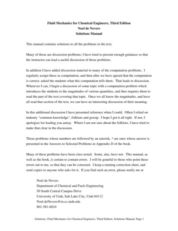
IBASIC SEMICONDUCTOR THEORYIf we reverse the polarity of the battery as in Figure 3 we have the followingsituation: pBN FIGURE 3Now the positive and negative particles are drawn away from the junction by thebattery's voltage, leaving the section of the crystal near the junction practically voidof charge carriers and crystal effectively blocks current. A few random charge carriersdo remain in the junction area allowing a minute current to pass. This current is knownas "leakage current" and is usually in the order of a few microamperes.We have seen how semiconductors are capable of rectifying current by the use of asingle junction within a crystal. By adding a second junction and making a P-N-P orN-P-N sandwich of N and P types we have a device capable of amplification knownas a transistor.The transistor may be compared to a triode tube in some ways, so let's quicklyreview the triode tube. The tube represented in Figure 4 has three distinct elements:(IfFIGURE 41. The cathode, which emits electrons; 2. The plate which collects the emitted electrons, and 3. The control grid, which controls the charge concentration -of the spacesA and B separating the elements by altering the charge of these spaces. When a largefixed voltage is applied between the cathode and plate and a small varying voltageis applied to the control grid, the plate current varies as much as it would if we madelarge changes in the plate voltage, giving us a device capable of amplifying voltage.Now consider the transistor. Again we have three elements, separated by junctionsas shown in Figure 5.NEMITTERBASEFIGURE 56COLLECTOR IIIII-
BASIC SEMICONDUCTOR THEORYHere the emitter emits electrons, the collector collects electrons and the base controlsthe flow of electrons by controlling the charge concentration in the base region, · soin the broadest sense, the function of the three elements in the triode tube and the transistor are similar. However, in the transistor we are amplifying current, not voltage, andits operation is not really as analogous to the tube's operation as this comparison shows.Let's look a little closer at how a transistor works. First of all we will put thetransistor in a circuit as in Figure 6 .EMITTER JUNCTIONCOLLECTOR JUNCTIONNEMITTERNBA SECOLLECTOR . FIGURE 6Here we see that the emitter junction will pass current easily, because it has a forwardbias. The collector junction however, will not pass current from the collector to base,because this junction is back biased. These bias conditions are necessary for transistoroperation. It is found that the majority of the current flows between the emitter and thecollector because of the large number of electrons from the emitter which diffusethrough the very thin base region and into the collector without combining with theholes in the base. As the base is made more positive, more electrons are pulled out ofthe emitter and are made available for diffusion into the collector.If the base is made less positive, less electrons are pulled from the emitter, so lessreach the collector. The electrons that enter the base, but do not reach the collector,combine with holes in the base and contribute to the base current, reducing the gainof the transistor. To reduce the base current, the base is kept as thin as possible(usually less than a thousandths of an inch thick) and the hole content kept to a minimum by using high-purity material, or in other words, the base material is only slightly"p" type material.The ratio of the collector current to the base current is called beta, usually shownon specification sheets as hFE, and the ratio of the collector current to the emittercurrent is called alpha, usually shown as hFB. Of course it is desirable to have the alphaof a transistor as high as possible and alphas of 0.95 to 0.99 are common in commercial transistors.No current (except a small leakage current) will flow in the collector circuit unlesscurrent is introduced into the emitter. Since very little voltage (.1 to .5 volts) is neededto cause appreciable current flow into the emitter, the input power is very low. Almostall the emitter current (emitter current times alpha) will flow in the collector circuitwhere the voltage can be as high as 45 volts. Therefore, a relatively large amount ofpower can be controlled in an external load and the power gain (Ge) of a transistor(power out/power in) can be up to 40,000 in some applications.7
TRANSISTOR CONSTRUCTION TECHNIQUESThe most common type of junction transistor is the PNP diffused alloyed type.This transistor is made by taking a wafer of "N" type germanium, mounting it on aholder and pressing indium dots into each side. The assembly is then heated in afurnace until the indium melts and alloys with the germanium forming a "P" layerwithin the "N" type germanium. The complete assembly is shown by Figure 7.fiIFIGURE 7By changing the size of the indium dots and the depth to which the indium isalloyed into the base material, it is possible to obtain a transistor optimized either foraudio amplifiers or high speed switching. In addition, by starting with P type germanium, it is possible to make a NPN transistor. With the alloy type of structure, it ispossible to pass currents of up to 112 an ampere through the transistor. This structureis not generally suitable for high frequency linear amplifiers since the indium dotsproduce a high capacitance between collector and base making the unit inherentlyunstable at high frequencies.The rate grown transistor is produced by an entirely different technique. A barof germanium is grown from a bath of molten germanium so doped that t
as a transistor. I The transistor may be compared to a triode tube in some ways, so let's quickly ( review the triode tube. The tube represented in Figure 4 has three distinct elements: I FIGURE 4 1. The cathode, which emits electrons; 2. The plate collects the emitted elec trons, and 3. The control grid, which controls the charge concentration -of the spaces