Transcription
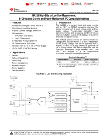
ProductFolderSample &BuySupport &CommunityTools OS547A – JUNE 2011 – REVISED AUGUST 2015INA226 High-Side or Low-Side Measurement,Bi-Directional Current and Power Monitor with I2C Compatible Interface1 Features3 Description The INA226 is a current shunt and power monitorwith an I2C - or SMBUS-compatible interface. Thedevice monitors both a shunt voltage drop and bussupply voltage. Programmable calibration value,conversion times, and averaging, combined with aninternal multiplier, enable direct readouts of current inamperes and power in watts.1 Senses Bus Voltages From 0 V to 36 VHigh-Side or Low-Side SensingReports Current, Voltage, and PowerHigh Accuracy:– 0.1% Gain Error (Max)– 10 μV Offset (Max)Configurable Averaging Options16 Programmable AddressesOperates from 2.7-V to 5.5-V Power Supply10-Pin, DGS (VSSOP) PackageThe INA226 senses current on common-mode busvoltages that can vary from 0 V to 36 V, independentof the supply voltage. The device operates from asingle 2.7-V to 5.5-V supply, drawing a typical of 330μA of supply current. The device is specified over theoperating temperature range between –40 C and125 C and features up to 16 programmableaddresses on the I2C-compatible interface.2 Applications ServersTelecom EquipmentComputingPower ManagementBattery ChargersPower SuppliesTest EquipmentDevice Information(1)PART NUMBERINA226PACKAGEVSSOP (10)BODY SIZE (NOM)3.00 mm x 3.00 mm(1) For all available packages, see the orderable addendum atthe end of the datasheet.High-Side or Low-Side Sensing ApplicationPower Supply(0 V to 36 V)CBYPASS0.1 mFHighSideShuntVS(Supply Voltage)VBUSSDASCL LoadPower RegisterV2VIN LowSideShuntCurrent RegisterADCIVIN–Voltage RegisterI C or SMBusCompatibleInterfaceAlertA0Alert RegisterA1GND1An IMPORTANT NOTICE at the end of this data sheet addresses availability, warranty, changes, use in safety-critical applications,intellectual property matters and other important disclaimers. PRODUCTION DATA.
INA226SBOS547A – JUNE 2011 – REVISED AUGUST 2015www.ti.comTable of Contents1234567Features .Applications .Description .Revision History.Pin Configuration and Functions lute Maximum Ratings .ESD Ratings.Recommended Operating Conditions.Thermal Information .Electrical Characteristics.Typical Characteristics .Detailed Description . 107.17.27.37.4Overview .Functional Block Diagram .Feature Description.Device Functional Modes.101010137.5 Programming . 157.6 Register Maps . 218Application and Implementation . 288.1 Application Information. 288.2 Typical Applications . 289 Power Supply Recommendations. 3010 Layout. 3010.1 Layout Guidelines . 3010.2 Layout Example . 3011 Device and Documentation Support . 3111.111.211.311.411.5Device Support .Community Resources.Trademarks .Electrostatic Discharge Caution .Glossary .313131313112 Mechanical, Packaging, and OrderableInformation . 314 Revision HistoryChanges from Original (June 2011) to Revision A 2PageAdded Handling Rating table, Feature Description section, Device Functional Modes, Application andImplementation section, Power Supply Recommendations section, Layout section, Device and DocumentationSupport section, and Mechanical, Packaging, and Orderable Information section . 1Submit Documentation FeedbackCopyright 2011–2015, Texas Instruments IncorporatedProduct Folder Links: INA226
INA226www.ti.comSBOS547A – JUNE 2011 – REVISED AUGUST 20155 Pin Configuration and FunctionsDGS Package10-Pin VSSOPTop ViewA1 110 IN A029 IN–Alert38 VBUSSDA47 GNDSCL56 VSPin FunctionsPINNAMENO.I/ODESCRIPTIONA02Digital inputAddress pin. Connect to GND, SCL, SDA, or VS. Table 2 shows pin settings and corresponding addresses.A11Digital inputAddress pin. Connect to GND, SCL, SDA, or VS. Table 2 shows pin settings and corresponding addresses.Alert3Digital outputGND7AnalogIN 10Analog inputConnect to supply side of shunt resistor.IN–9Analog inputConnect to load side of shunt resistor.SCL5Digital inputSerial bus clock line, open-drain input.SDA4Digital I/OVBUS8Analog inputVS6AnalogMulti-functional alert, open-drain output.Ground.Serial bus data line, open-drain input/output.Bus voltage input.Power supply, 2.7 V to 5.5 V.Submit Documentation FeedbackCopyright 2011–2015, Texas Instruments IncorporatedProduct Folder Links: INA2263
INA226SBOS547A – JUNE 2011 – REVISED AUGUST 2015www.ti.com6 Specifications6.1 Absolute Maximum Ratingsover operating free-air temperature range (unless otherwise noted)(1)MINVVSMAXUNIT6VSupply voltage–4040–0.340VVBUS–0.340VVSDAGND – 0.36VVSCLGND – 0.3VVS 0.3V5mAAnalog Inputs,IN , IN–Differential (VIN – VIN-)(2)Common-Mode (VIN VIN-) / 2VIINInput current into any pinIOUTOpen-drain digital output current10mATJJunction temperature150 CTstgStorage temperature range150 C(1)(2)–65Stresses beyond those listed under Absolute Maximum Ratings may cause permanent damage to the device. These are stress ratingsonly, which do not imply functional operation of the device at these or any other conditions beyond those indicated under RecommendedOperating Conditions. Exposure to absolute-maximum-rated conditions for extended periods may affect device reliability.IN and IN– may have a differential voltage between –40 V and 40 V. However, the voltage at these pins must not exceed the range–0.3 V to 40 V.6.2 ESD RatingsVALUEHuman body model (HBM), per ANSI/ESDA/JEDEC JS-001, all pinsElectrostaticdischargeV(ESD)(1)(2)(1)UNIT 2500Charged device model (CDM), per JEDEC specification JESD22-C101, allpins (2) 1000Machine model (MM) 150VJEDEC document JEP155 states that 500-V HBM allows safe manufacturing with a standard ESD control process.JEDEC document JEP157 states that 250-V CDM allows safe manufacturing with a standard ESD control process.6.3 Recommended Operating Conditionsover operating free-air temperature range (unless otherwise noted)MINNOMVCMCommon-mode input voltage12VVSOperating supply voltage3.3TAOperating free-air temperatureMAXUNITVV–40125 C6.4 Thermal InformationINA226THERMAL METRIC(1)DGS (VSSOP)UNIT10 PINSRθJAJunction-to-ambient thermal resistance171.4 C/WRθJC(top)Junction-to-case (top) thermal resistance42.9 C/WRθJBJunction-to-board thermal resistance91.8 C/WψJTJunction-to-top characterization parameter1.5 C/WψJBJunction-to-board characterization parameter90.2 C/WRθJC(bot)Junction-to-case (bottom) thermal resistancen/a C/W(1)4For more information about traditional and new thermal metrics, see the Semiconductor and IC Package Thermal Metrics applicationreport, SPRA953.Submit Documentation FeedbackCopyright 2011–2015, Texas Instruments IncorporatedProduct Folder Links: INA226
INA226www.ti.comSBOS547A – JUNE 2011 – REVISED AUGUST 20156.5 Electrical CharacteristicsTA 25 C, VVS 3.3 V, VIN 12 V, VSENSE (VIN – VIN–) 0 mV and VVBUS 12 V, unless otherwise notedPARAMETERTEST CONDITIONSMINTYPMAXUNITmVINPUTShunt voltage input range–81.917581.92Bus voltage input range (1)0360 V VIN 36 VCMRRCommon-mode rejectionVOSShunt offset voltage, RTI (2)PSRRVOSShunt offset voltage, RTI (2) vstemperature–40 C TA 125 CShunt offset voltage, RTI (2) vsPower supply2.7 V VS 5.5 VBus offset voltage, RTI(2)Bus offset voltage, RTI (2) vstemperature(2)PSRRBus offset voltage, RTIsupplyIBInput bias current (IIN , IIN– pins)–40 C TA 125 Cvs powerVBUS input impedanceInput leakage(3)126V140dB 2.5 10μV0.020.1μV/ CμV/V2.5 1.25 7.51040mVμV/ C0.5mV/V10μA830kΩ(IN pin) (IN– pin),Power-down mode0.116BitsShunt voltage2.5μVμA0.5DC ACCURACYADC native resolution1 LSB step sizeBus voltageShunt voltage gain errorShunt voltage gain error vstemperature–40 C TA 125 CBus voltage gain errorBus voltage gain error vstemperature–40 C TA 125 CDifferential nonlinearitytCTADC conversion time1.25mV0.02%0.1%10500.02%0.1%1050 0.1ppm/ Cppm/ CLSBCT bit 000140154CT bit 001204224CT bit 010332365CT bit 011588646CT bit 1001.11.21CT bit 1012.1162.328CT bit 1104.1564.572CT bit 1118.2449.0682835μsmsSMBusSMBus timeout (4)(1)(2)(3)(4)msWhile the input range is 36 V, the full-scale range of the ADC scaling is 40.96 V. See the Basic ADC Functions section. Do not applymore than 36 V.RTI Referred-to-input.Input leakage is positive (current flowing into the pin) for the conditions shown at the top of this table. Negative leakage currents canoccur under different input conditions.SMBus timeout in the INA226 resets the interface any time SCL is low for more than 28 ms.Submit Documentation FeedbackCopyright 2011–2015, Texas Instruments IncorporatedProduct Folder Links: INA2265
INA226SBOS547A – JUNE 2011 – REVISED AUGUST 2015www.ti.comElectrical Characteristics (continued)TA 25 C, VVS 3.3 V, VIN 12 V, VSENSE (VIN – VIN–) 0 mV and VVBUS 12 V, unless otherwise notedPARAMETERTEST CONDITIONSMINTYPMAXUNITDIGITAL INPUT/OUTPUTInput capacitanceLeakage input current30 V VSCL VVS ,0 V VSDA VVS,0 V VAlert VVS ,0 V VA0 VVS ,0 V VA1 VVS0.1pF1μAVIHHigh-level input voltage0.7 VVS6VVILLow-level input voltage–0.50.3 VVSVVOLLow-level output voltage, SDA, Alert00.4IOL 3 mAHysteresis500VmVPOWER SUPPLYOperating supply rangeIQVPOR65.5VQuiescent current2.7330420μAQuiescent current, power-down(shutdown) mode0.52μAPower-on reset threshold2Submit Documentation FeedbackVCopyright 2011–2015, Texas Instruments IncorporatedProduct Folder Links: INA226
INA226www.ti.comSBOS547A – JUNE 2011 – REVISED AUGUST 20156.6 Typical CharacteristicsAt TA 25 C, VVS 3.3 V, VIN 12 V, VSENSE (VIN – VIN–) 0 mV and VVBUS 12 V, unless otherwise noted.0 10PopulationGain (dB) 20 30 40G00110864Input Offset Voltage (mV)Figure 2. Shunt Input Offset Voltage Production DistributionFigure 1. Frequency Response170Common Mode Rejection Ratio (dB) 1 1.2 1.4Offset (µV)2100k010k-21001kFrequency (Hz)-410-61-10 60-8 50 1.6 1.8 2 2.2 2.4 50 2502550Temperature ( C)75100160150140 50125 250G003Figure 3. Shunt Input Offset Voltage vs Temperature2550Temperature ( C)75100125G004Figure 4. Shunt Input Common-Mode Rejection Ratio vsTemperature600PopulationGain Error (m%)500400300200100806040200-20-40-60-80-1001000 50 2502550Temperature ( C)75100125G007Input Gain Error (m%)Figure 5. Shunt Input Gain Error Production DistributionFigure 6. Shunt Input Gain Error vs TemperatureSubmit Documentation FeedbackCopyright 2011–2015, Texas Instruments IncorporatedProduct Folder Links: INA2267
INA226SBOS547A – JUNE 2011 – REVISED AUGUST 2015www.ti.comTypical Characteristics (continued)At TA 25 C, VVS 3.3 V, VIN 12 V, VSENSE (VIN – VIN–) 0 mV and VVBUS 12 V, unless otherwise noted.300200PopulationGain Error Common Mode Input Voltage (V)-34-4.50-7.5 50-60Input Offset Voltage (mV)Figure 8. Bus Input Offset Voltage Production DistributionFigure 7. Shunt Input Gain Error vs Common-Mode Voltage 0.6PopulationOffset (mV) 0.8 1.0G00910080604012520100075-202550Temperature ( C)-400-60 25-100 1.4 50-80 1.2Input Gain Error (m%)Figure 10. Bus Input Gain Error Production DistributionFigure 9. Bus Input Offset Voltage vs Temperature60025Input Bias Current (µA)Gain Error (m%)5004003002001000 50 2502550Temperature ( C)751001510500G012Figure 11. Bus Input Gain Error vs Temperature812520481216202428Common Mode Input Voltage (V)3236G012Figure 12. Input Bias Current vs Common-Mode VoltageSubmit Documentation FeedbackCopyright 2011–2015, Texas Instruments IncorporatedProduct Folder Links: INA226
INA226www.ti.comSBOS547A – JUNE 2011 – REVISED AUGUST 2015Typical Characteristics (continued)At TA 25 C, VVS 3.3 V, VIN 12 V, VSENSE (VIN – VIN–) 0 mV and VVBUS 12 V, unless otherwise noted.260Input Bias Current Shutdown (nA)Input Bias Current (µA)2422201816 50 2502550Temperature ( C)7510014010060 250G013Figure 13. Input Bias Current vs Temperature2550Temperature ( C)75100125G014Figure 14. Input Bias Current vs Temperature, Shutdown1.2Quiescent Current Shutdown (µA)Quiescent Current (µA)18020 50125500400300200100 50220 2502550Temperature ( C)7510010.80.60.40.2 50125 250G015Figure 15. Active IQ vs Temperature2550Temperature ( C)75100125G016Figure 16. Shutdown IQ vs Temperature500300250Shutdown IQ (mA)IQ 01,00010,000Frequency (kHz)Frequency (kHz)Figure 17. Active IQ vs I2C Clock FrequencyFigure 18. Shutdown IQ vs I2C Clock FrequencySubmit Documentation FeedbackCopyright 2011–2015, Texas Instruments IncorporatedProduct Folder Links: INA2269
INA226SBOS547A – JUNE 2011 – REVISED AUGUST 2015www.ti.com7 Detailed Description7.1 OverviewThe INA226 is a digital current sense amplifier with an I2C- and SMBus-compatible interface. It provides digitalcurrent, voltage, and power readings necessary for accurate decision-making in precisely-controlled systems.Programmable registers allow flexible configuration for measurement resolution as well as continuous-versustriggered operation. Detailed register information appears at the end of this data sheet, beginning with Table 4.See the Functional Block Diagram section for a block diagram of the INA226 device.7.2 Functional Block DiagramPower(1)Bus Voltage(1) Shunt VoltageChannelCurrent(1)ADCBus VoltageChannelCalibration(2) Shunt Voltage(1)Data Registers(1) Read-only(2) Read/write7.3 Feature Description7.3.1 Basic ADC FunctionsThe INA226 device performs two measurements on the power-supply bus of interest. The voltage developedfrom the load current that flows through a shunt resistor creates a shunt voltage that is measured at the IN andIN– pins. The device can also measure the power supply bus voltage by connecting this voltage to the VBUS pin.The differential shunt voltage is measured with respect to the IN– pin while the bus voltage is measured withrespect to ground.The device is typically powered by a separate supply that can range from 2.7 V to 5.5 V. The bus that is beingmonitored can range in voltage from 0 V to 36 V. Based on the fixed 1.25-mV LSB for the Bus Voltage Registerthat a full-scale register results in a 40.96 V value.NOTEDo not apply more than 36 V of actual voltage to the input pins.There are no special considerations for power-supply sequencing because the common-mode input range andpower-supply voltage are independent of each other; therefore, the bus voltage can be present with the supplyvoltage off, and vice-versa.The device takes two measurements, shunt voltage and bus voltage. It then converts these measurements tocurrent, based on the Calibration Register value, and then calculates power. Refer to the Programming theCalibration Register section for additional information on programming the Calibration Register.10Submit Documentation FeedbackCopyright 2011–2015, Texas Instruments IncorporatedProduct Folder Links: INA226
INA226www.ti.comSBOS547A – JUNE 2011 – REVISED AUGUST 2015Feature Description (continued)The device has two operating modes, continuous and triggered, that determine how the ADC operates followingthese conversions. When the device is in the normal operating mode (that is, MODE bits of the ConfigurationRegister (00h) are set to '111'), it continuously converts a shunt voltage reading followed by a bus voltagereading. After the shunt voltage reading, the current value is calculated (based on Equation 3). This current valueis then used to calculate the power result (using Equation 4). These values are subsequently stored in anaccumulator, and the measurement/calculation sequence repeats until the number of averages set in theConfiguration Register (00h) is reached. Following every sequence, the present set of values measured andcalculated are appended to previously collected values. After all of the averaging has been completed, the finalvalues for shunt voltage, bus voltage, current, and power are updated in the corresponding registers that canthen be read. These values remain in the data output registers until they are replaced by the next fully completedconversion results. Reading the data output registers does not affect a conversion in progress.The mode control in the Conversion Register (00h) also permits selecting modes to convert only the shuntvoltage or the bus voltage in order to further allow the user to configure the monitoring function to fit the specificapplication requirements.All current and power calculations are performed in the background and do not contribute to conversion time.In triggered mode, writing any of the triggered convert modes into the Configuration Register (00h) (that is,MODE bits of the Configuration Register (00h) are set to ‘001’, ‘010’, or ‘011’) triggers a single-shot conversion.This action produces a single set of measurements; thus, to trigger another single-shot conversion, theConfiguration Register (00h) must be written to a second time, even if the mode does not change.In addition to the two operating modes (continuous and triggered), the device also has a power-down mode thatreduces the quiescent current and turns off current into the device inputs, reducing the impact of supply drainwhen the device is not being used. Full recovery from power-down mode requires 40µs. The registers of thedevice can be written to and read from while the device is in power-down mode. The device remains in powerdown mode until one of the active modes settings are written into the Configuration Register (00h) .Although the device can be read at any time, and the data from the last conversion remain available, theConversion Ready flag bit (Mask/Enable Register, CVRF bit) is provided to help coordinate one-shot or triggeredconversions. The Conversion Ready flag (CVRF) bit is set after all conversions, averaging, and multiplicationoperations are complete.The Conversion Ready flag (CVRF) bit clears under these conditions: Writing to the Configuration Register (00h), except when configuring the MODE bits for power-down mode; or Reading the Mask/Enable Register (06h)7.3.1.1 Power CalculationThe Current and Power are calculated following shunt voltage and bus voltage measurements as shown inFigure 19. Current is calculated following a shunt voltage measurement based on the value set in the CalibrationRegister. If there is no value loaded into the Calibration Register, the current value stored is zero. Power iscalculated following the bus voltage measurement based on the previous current calculation and bus voltagemeasurement. If there is no value loaded in the Calibration Register, the power value stored is also zero. Again,these calculations are performed in the background and do not add to the overall conversion time. These currentand power values are considered intermediate results (unless the averaging is set to 1) and are stored in aninternal accumulation register, not the corresponding output registers. Following every measured sample, thenewly-calculated values for current and power are appended to this accumulation register until all of the sampleshave been measured and averaged based on the number of averages set in the Configuration Register (00h).Submit Documentation FeedbackCopyright 2011–2015, Texas Instruments IncorporatedProduct Folder Links: INA22611
INA226SBOS547A – JUNE 2011 – REVISED AUGUST 2015www.ti.comFeature Description (continued)Bus and Power Limit DetectFollowing Every Bus Voltage ConversionCurrent Limit Detect FollowingEvery Shunt Voltage VIPVIPVPPower AverageBus Voltage AverageShunt Voltage AverageFigure 19. Power Calculation SchemeIn addition to the current and power accumulating after every sample, the shunt and bus voltage measurementsare also collected. After all of the samples have been measured and the corresponding current and powercalculations have been made, the accumulated average for each of these parameters is then loaded to thecorresponding output registers, where they can then be read.7.3.1.2 Alert PinThe INA226 has a single Alert Limit Register (07h), that allows the Alert pin to be programmed to respond to asingle user-defined event or to a Conversion Ready notification if desired. The Mask/Enable Register allows theuser to select from one of the five available functions to monitor and/or set the Conversion Ready bit to controlthe response of the Alert pin. Based on the function being monitored, the user would then enter a value into theAlert Limit Register to set the corresponding threshold value that asserts the Alert pin.The Alert pin allows for one of several available alert functions to be monitored to determine if a user-definedthreshold has been exceeded. The five alert functions that can be monitored are: Shunt Voltage Over-Limit (SOL) Shunt Voltage Under-Limit (SUL) Bus Voltage Over-Limit (BOL) Bus Voltage Under-Limit (BUL) Power Over-Limit (POL)The Alert pin is an open-drain output. This pin is asserted when the alert function selected in the Mask/EnableRegister exceeds the value programmed into the Alert Limit Register. Only one of these alert functions can beenabled and monitored at a time. If multiple alert functions are enabled, the selected function in the highestsignificant bit position takes priority and responds to the Alert Limit Register value. For example, if the ShuntVoltage Over-Limit function and the Shunt Voltage Under-Limit function are both selected, the Alert pin assertswhen the Shunt Voltage Register exceeds the value in the Alert Limit Register.The Conversion Ready state of the device can also be monitored at the Alert pin to inform the user when thedevice has completed the previous conversion and is ready to begin a new conversion. Conversion Ready canbe monitored at the Alert pin along with one of the alert functions. If an alert function and the Conversion Readyare both enabled to be monitored at the Alert pin, after the Alert pin is asserted, the Mask/Enable Register mustbe read following the alert to determine the source of the alert. By reading the Conversion Ready Flag (CVRF, bit3), and the Alert Function Flag (AFF, bit 4) in the Mask/Enable Register, the source of the alert can bedetermined. If the Conversion Ready feature is not desired and the CNVR bit is not set, the Alert pin onlyresponds to an exceeded alert limit based on the alert function enabled.If the alert function is not used, the Alert pin can be left floating without impacting the operation of the device.12Submit Documentation FeedbackCopyright 2011–2015, Texas Instruments IncorporatedProduct Folder Links: INA226
INA226www.ti.comSBOS547A – JUNE 2011 – REVISED AUGUST 2015Feature Description (continued)Refer to Figure 19 to see the relative timing of when the value in the Alert Limit Register is compared to thecorresponding converted value. For example, if the alert function that is enabled is Shunt Voltage Over-Limit(SOL), following every shunt voltage conversion the value in the Alert Limit Register is compared to themeasured shunt voltage to determine if the measurements has exceeded the programmed limit. The AFF, bit 4 ofthe Mask/Enable Register, asserts high any time the measured voltage exceeds the value programmed into theAlert Limit Register. In addition to the AFF being asserted, the Alert pin is asserted based on the Alert Polarity Bit(APOL, bit 1 of the Mask/Enable Register). If the Alert Latch is enabled, the AFF and Alert pin remain asserteduntil either the Configuration Register (00h) is written to or the Mask/Enable Register is read.The Bus Voltage alert functions compare the measured bus voltage to the Alert Limit Register following everybus voltage conversion and assert the AFF bit and Alert pin if the limit threshold is exceeded.The Power Over-Limit alert function is also compared to the calculated power value following every bus voltagemeasurement conversion and asserts the AFF bit and Alert pin if the limit threshold is exceeded.7.4 Device Functional Modes7.4.1 Averaging and Conversion Time ConsiderationsThe INA226 device offers programmable conversion times (tCT) for both the shunt voltage and bus voltagemeasurements. The conversion times for these measurements can be selected from as fast as 140 μs to as longas 8.244 ms. The conversion time settings, along with the programmable averaging mode, allow the device to beconfigured to optimize the available timing requirements in a given application. For example, if a system requiresthat data be read every 5ms, the device could be configured with the conversion times set to 588 μs for bothshunt and bus voltage measurements and the averaging mode set to 4. This configuration results in the dataupdating approximately every 4.7ms. The device could also be configured with a different conversion time settingfor the shunt and bus voltage measurements. This type of approach is common in applications where the busvoltage tends to be relatively stable. This situation can allow for the time focused on the bus voltagemeasurement to be reduced relative to the shunt voltage measurement. The shunt voltage conversion time couldbe set to 4.156 ms with the bus voltage conversion time set to 588 μs, with the averaging mode set to 1. Thisconfiguration also results in data updating approximately every 4.7 ms.There are trade-offs associated with the settings for conversion time and the averaging mode used. Theaveraging feature can significantly improve the measurement accuracy by effectively filtering the signal. Thisapproach allows the device to reduce any noise in the measurement that may be caused by noise coupling intothe signal. A greater number of averages enables the device to be more effective in reducing the noisecomponent of the measurement.The conversion times selected can also have an impact on the measurement accuracy. Figure 20 shows multipleconversion times to illustrate the impact of noise on the measurement. In order to achieve the highest accuracymeasurement possible, use a combination of the longest allowable conversion times and highest number ofaverages, based on the timing requirements of the system.10mV/divConversion Time: 140msConversion Time: 1.1msConversion Time: 8.244ms02004006008001000Number of ConversionsFigure 20. Noise vs Conversion TimeSubmit Documentation FeedbackCopyright 2011–2015, Texas Instruments IncorporatedProduct Folder Links: INA22613
INA226SBOS547A – JUNE 2011 – REVISED AUGUST 2015www.ti.comDevice Functional Modes (continued)7.4.2 Filtering and Input ConsiderationsMeasuring current is often noisy, and such noise can be difficult to define. The INA226 device offers severaloptions for filtering by allowing the conversion times and number of averages to be selected independently in theConfiguration Register (00h). The conversion times can be set independently for the shunt voltage and busvoltage measurements to allow added flexibility in configuring the monitoring of the power-supply bus.The internal ADC is based on a delta-sigma (ΔΣ) front-end with a 500 kHz ( 30%) typical sampling rate. Thisarchitecture has good inherent noise rejection; however, transients that occur at or very close to the samplingrate harmonics can cause problems. Because these signals are at 1 MHz and higher, they can be managed byincorporating filtering at the input of the device. The high frequency enables the use of low-value series resistorson the filter with negligible effects on measurement accuracy. In general, filtering the device input is onlynecessary if there are transients at exact harmonics of the 500 kHz ( 30%) sampling rate (greater than 1 MHz).Filter using the lowest possible series resistance (typically 10 Ω or less) and a ceramic capacitor. Recommendedvalues for this capacitor are between 0.1 μF and 1 μF. Figure 21 shows the device with a filter added at theinput.Overload conditions are another consideration for the device inputs. The device inputs are specified to tolerate40 V across the inputs. A large differential scenario might be a short to ground on the load side of the shunt. Thistype of event can result in full power-supply voltage across the shunt (as long the power supply or energystorage capacitors support it). Removing a short to ground can result in inductive kickbacks that could exceedthe 40-V differential and common-mode rating of the device. Inductive kickback voltages are best controlled byZener-type transient-absorbing devices (commonly called transzorbs) combined with sufficient energy storagecapacita
INA226 www.ti.com SBOS547A -JUNE 2011-REVISED AUGUST 2015 6.5 Electrical Characteristics TA 25 C, VVS 3.3 V, VIN 12 V, VSENSE (VIN - VIN-) 0 mV and VVBUS 12 V, unless otherwise noted PARAMETER TEST CONDITIONS MIN TYP MAX UNIT INPUT Shunt voltage input range -81.9175 81.92 mV Bus voltage input range(1) 0 36 V CMRR Common-mode rejection 0 V VIN 36 V 126 140 dB