Transcription
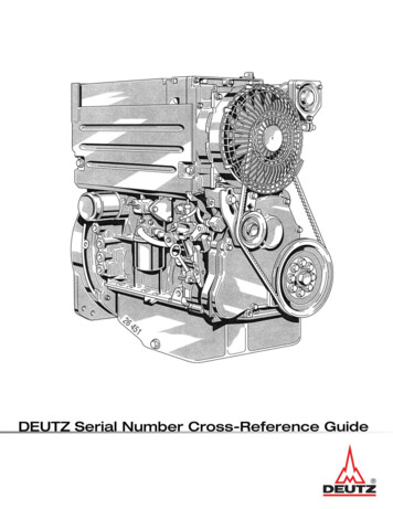
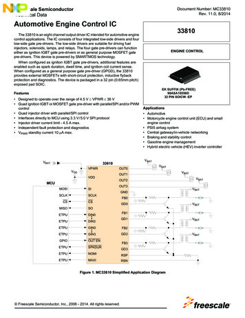
Freescale Semiconductor Technical DataDocument Number: MC33810Rev. 11.0, 8/2014Automotive Engine Control IC33810The 33810 is an eight channel output driver IC intended for automotive enginecontrol applications. The IC consists of four integrated low-side drivers and fourlow-side gate pre-drivers. The low-side drivers are suitable for driving fuelinjectors, solenoids, lamps, and relays. The four gate pre-drivers can functioneither as ignition IGBT gate pre-drivers or as general purpose MOSFET gatepre-drivers. This device is powered by SMARTMOS technology.When configured as ignition IGBT gate pre-drivers, additional features areenabled such as spark duration, dwell time, and ignition coil current sense.When configured as a general purpose gate pre-driver (GPGD), the 33810provides external MOSFETs with short-circuit protection, inductive flybackprotection and diagnostics. The device is packaged in a 32 pin (0.65mm pitch)exposed pad SOIC.ENGINE CONTROLEK SUFFIX (Pb-FREE)98ASA10556D32 PIN SOICW -EPFeatures Designed to operate over the range of 4.5 V VPWR 36 V Quad ignition IGBT or MOSFET gate pre-driver with parallel/SPI and/or PWMcontrol Quad injector driver with parallel/SPI control Interfaces directly to MCU using 3.3 V / 5.0 V SPI protocol Injector driver current limit - 4.5 A max. Independent fault protection and diagnostics VPWR standby current 10 A SOSOETPUDIN0Applications Automotive Motorcycle engine control unit (ECU) and smallengine control PSI5 airbag system Central gateway/in-vehicle networking Braking and stability control Gasoline engine management Hybrid electric vehicle (HEV) inverter TFB1GD1ETPUDIN3ETPUGIN0FB2ETPUGIN3GD2GPIOOUT ENETPUSPKDURETPUNOMIETPUMAXIFB3GD3RSPRSNFigure 1. MC33810 Simplified Application Diagram Freescale Semiconductor, Inc., 2006 - 2014. All rights reserved.VBATVBATVBAT
ORDERABLE PARTSORDERABLE PARTSThis section describes the part numbers available to be purchased along with their differences. Valid orderable part numbers areprovided on the web. To determine the orderable part numbers for this device, go to http://www.freescale.com and perform a part numbersearch for the following device numbers.Table 1. Orderable Part VariationsPart NumberMCZ33810EKNotesTemperature (TA)(1)-40 C to 125 CPackage32 SOICW-EPNotes1. To order parts in Tape & Reel, add the R2 suffix to the part number.338102Analog Integrated Circuit Device Data Freescale Semiconductor
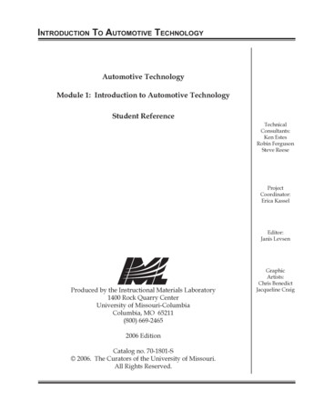
INTERNAL BLOCK DIAGRAMINTERNAL BLOCK DIAGRAMVPWRVDDVDDVDD 50 µA 50 µACSSISCLKOUTENVPWR, VDDV8.0 AnalogV2.5 LogicPOR, OvervoltageUndervoltageLOGIC CONTROL 15 µAVDD 15 T2OUT3Outputs 0 to 3SOGate ControlDIN0 50 µAPARALLELCONTROLVOC1DIN1 – 50 µARSlLimitExposedPadPWMCONTROLLERDIN275 µACurrent LimitTemperature LimitShort/Open 50 µA 50 µANOMI,MAXIDACSPARK DURATION –SPI –SPIGIN0Open Secondary 50 µASPARKDACGIN1 VPWR FB0FB1FB2FB3100 µAVLVCDIN3VOCGPGDOnly 50 µAGATE DRIVECONTROLGIN2 50 µANOMI –DAC –DAC 5 0µASPKDURMAXIGPGDClampGD0GD1GD2GD3GIN3 50 µAVDDLow VClampRSPRSNNOMIMAXIExposed PadGNDFigure 2. 33810 Simplified Internal Block Diagram33810Analog Integrated Circuit Device Data Freescale Semiconductor3
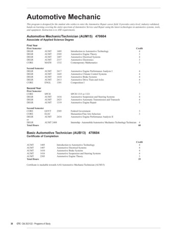
PIN CONNECTIONSPIN CONNECTIONSTransparent Top N1GIN2GIN3SPKDURGD3FB3OUT3Figure 3. 33810 Pin ConnectionsA functional description of each pin can be found in the Functional Pin Description section beginning on page 14.Table 2. 33810 Pin DefinitionsPin NumberPin NamePin FunctionFormal NameDefinition1, 16, 32, 17OUT0, OUT1,OUT2, OUT3OutputLow-side InjectorDriver OutputThese pins are the Open drain low-side injector driver outputs.2, 15, 31, 18FB0, FB1,FB2, FB3InputFeedback VoltageSenseIn IGBT ignition gate pre-driver mode, these feedback inputs monitor the IGBT'scollector voltage to provide the spark duration timer control signal.3, 14, 30,19GD0, GD1,GD2, GD3OutputGate Drive OutputIGBT/GPGD outputs are controlled by GIN0 - 3. Pull-up and pull-down currentsources are used to provide a controlled slew rate to an external IGBT or MOSFETconnected as a low-side driver.4CSInputChip SelectThe Chip Select input pin is an active low signal sent by the MCU to indicate thedevice is being addressed. This input requires CMOS logic levels and has aninternal active pull-up current source.5SCLKInputSerial Clock InputThe SCLK input pin is used to clock the serial data on the SI and SO pins in andout while being addressed by the CS.6SIInputSerial Input DataThe SI input pin is used to receive serial data from the MCU.7SOOutputSerial Output DataThe SO output pin is used to transmit serial data from the device to the MCU.8VDDInputDigital Logic SupplyVoltageThe VDD input supply voltage determines the interface voltage levels between thedevice and the MCU, and is used to supply power to the Serial Out buffer (SO),SPKDUR buffer, MAXI, NOMI, and pull-up current source for the Chip Select (CS).9OUTENInputOutput EnableThe Output Enable pin (OUTEN) is an active low input. When the OUTEN pin is low,the device outputs are active. The outputs are disabled when OUTEN is high.10, 11, 12, 13DIN0,DIN1,DIN2,DIN3InputDriver Input 0, DriverInput 1, Driver Input 2,Driver Input 320SPKDUROutput24, 23, 22, 21GIN0,GIN1,GIN2,GIN3Input25VPWRInputActive high input control for injector outputs OUT0 - 3. The parallel input data islogically ORed with the corresponding SPI input data register contents.This pin is the Spark Duration Output. This open drain output is low while feedbackSpark Duration Output inputs FB0 - 3 are above the programmed spark detection threshold.Gate Driver Input 0Gate Driver Input 1Gate Driver Input 2Gate Driver Input 3These pins are the active high input control for IGBT/GPGD outputs GD0 - 3. Theparallel input data is logically ORed with the corresponding SPI input data registercontents in GPGD mode only.Analog Supply Voltage VPWR is the main voltage input for all internal analog bias circuitry.338104Analog Integrated Circuit Device Data Freescale Semiconductor
PIN CONNECTIONSTable 2. 33810 Pin Definitions (continued)Pin NumberPin NamePin FunctionFormal Name26RSPInputResistor SensePositiveThis pin is the Positive input of a current sense amplifier.27RSNInputResistor SenseNegativeThis pin is the Negative input of a current sense amplifier.28NOMIOutputNominal Ignition CoilCurrentThis pin is the Nominal Ignition Coil Current output flag. This output is assertedwhen the IGBT Collector-Emitter current exceeds the level selected by the DAC.OutputMaximum Ignition CoilCurrentThis pin is the Maximum Ignition Coil Current output flag. This output is assertedwhen the IGBT Collector-Emitter current exceeds the selected level of the DAC.This signal also latches off the gate pre-drive outputs when configured as a GPGD.The MAXI current level is determined by the voltage drop across an external senseresistor connected to pins RSP and RSN.GroundThe exposed pad is the only ground reference for analog, digital and power groundconnections. As such, it must be soldered directly to a low-impedance ground planefor both electrical and thermal considerations. For more information about thispackage, see application note AN2409 on the Freescale web site,www.freescale.com29Exposed Pad(bottom ofpackage)MAXIGNDGroundDefinition33810Analog Integrated Circuit Device Data Freescale Semiconductor5
ELECTRICAL CHARACTERISTICSMAXIMUM RATINGSELECTRICAL CHARACTERISTICSMAXIMUM RATINGSTable 3. Maximum RatingsAll voltages are with respect to ground unless otherwise noted.SymbolRatingsValueUnitNotesVPWR Supply Voltage-1.5 to 45VDC(1)VDDVDD Supply Voltage-0.3 to 7.0VDC(1)VILVIHSPI Interface and Logic Input Voltage (CS, SI, SO, SCLK, OUTEN, DIN0 - DIN3,GIN0 - GIN3, SPKDUR, NOMI, MAXI, RSP,RSN)-0.3 to VDDVDCVFBIGBT/GPGD Drain Voltage (VFB0 to VFB3)-1.5 to 60VDCInjector Output Voltage (OUTx)-1.5 to 60VDCGPGD Output Voltage (GDx)ELECTRICAL RATINGSVPWRVOUTXVGDx-0.3 to 10VDCECLAMPOutput Clamp Energy (OUT0 to OUT3)(Single Pulse)TJUNCTION 150 C, IOUT 1.5 A100mJECLAMPOutput Clamp Energy (OUT0 to OUT3)(Continuous Pulse)TJUNCTION 125 C, IOUT 1.0 A (Max Injector frequency is 70 Hz)100mJIOSSSSOutput Continuous Current (OUT0 to OUT3)TJUNCTION 150 C2.0AVRSXMaximum Voltage for RSN and RSP inputs-0.3 - VDDVDC–Frequency of SPI Operation (VDD 5.0 V)6.0MHzVESD1VESD2VESD3ESD VoltageHuman Body Model (HBM)Machine Model (MM)Charge Device Model (CDM) 2000 200 750V(2), (3)THERMAL RATINGSTATJTCTSTGPDTSOLDERR JAR JLR JCOperating TemperatureAmbientJunction2Case-40 to 125-40 to 150-40 to 125 CStorage Temperature-55 to 150 CPower Dissipation (TA 25 C)1.7WPeak Package Flow Temperature During Solder MountingEW Suffix245Thermal ResistanceJunction-to-AmbientJunction- to-LeadJunction-to-Flag758.01.2 C C/WNotes1. Exceeding these limits may cause malfunction or permanent damage to the device.2. ESD data available upon request.3. ESD testing is performed in accordance with the Human Body Model (HBM) (AEC-Q100-002), the Machine Model (MM) (AEC-Q100-003), andthe Charge Device Model (CDM), Robotic (AEC-Q100-011).338106Analog Integrated Circuit Device Data Freescale Semiconductor
ELECTRICAL CHARACTERISTICSSTATIC ELECTRICAL CHARACTERISTICSSTATIC ELECTRICAL CHARACTERISTICSTable 4. Static Electrical CharacteristicsCharacteristics noted under conditions of 3.0 V VDD 5.5 V, 6.0 V VPWR 32 V, -40 C TC 125 C, and calibrated timers, unlessotherwise noted. Typical values reflect the parameter’s approx. average value with VPWR 13 V, TA 25 ��3632V(4)POWER INPUT (VDD, VPWR)VPWR (FO)Supply VoltageFully Operational Full Parameter SpecificationIVPWR (ON)Supply CurrentAll Outputs Disabled (Normal mode)–10.014.0mAIVPWR (SS)Sleep State Supply Current (Must have VDD 0.8 V for Sleep state),VPWR 32 V–1530 AVPWR(OV)VPWR Overvoltage Shutdown Threshold Voltage36.53942VVPWR(OV-HYS)VPWR Overvoltage Shutdown Hysteresis Voltage0.51.53.0VVPWR(UV)VPWR Undervoltage Shutdown Threshold Voltage3.04.04.4VVPWR(UV-HYS)VPWR Undervoltage Shutdown Hysteresis Voltage100200300mVVPWR Low Operating Voltage (Low-voltage reported via the SPI)5.3–8.99VVDDVDD Supply Voltage3.0–5.5VIVDDVDD Supply CurrentStatic condition and does not include VDD current out of �–VPWR(LOV)VDD(UV)VDD Supply Undervoltage (Sleep state) Threshold Voltage(5)(6)(7)(8)INJECTOR DRIVER OUTPUTS (OUT 0:3)RDS (ON)Drain-to-Source ON ResistanceIOUT 1.0 A, TJ 125 C, VPWR 13 V IOUT 1.0 A, TJ 25 C, VPWR 13 V IOUT 1.0 A, TJ -40 C, VPWR 13 VIOUT (LIM)Output Self Limiting Current3.0–6.0AOutput Fault Detection Voltage ThresholdOutputs Programmed OFF (Open Load)Outputs Programmed ON (Short to Battery)2.02.53.0V40407575115115 AVOUT(FLT-TH) I(OFF)OCOOutput OFF Open Load Detection CurrentVDRAIN 18 V, Outputs Programmed OFFI(ON)OCOOutput ON Open Load Detection CurrentCurrent less then specification value considered open20100200mAOutput Clamp Voltage 1ID 20 mA485358VVOC1VDRAIN 32 V, Outputs Programmed OFF (-40 C)(9)Notes4. These parameters are guaranteed by design but not production tested. Fully operational means driver outputs toggle as expected with inputtoggling. SPI is guaranteed to be operational when VPWR 4.5 V. SPI may not report correctly when VPWR 4.5 V.5.6.7.Overvoltage thresholds minimum and maximum include hysteresis.Undervoltage thresholds minimum and maximum include hysteresis.Device is functional provided TJ is less than 150 C. Some table parameters may be out of specification.8.9.Device in Sleep state, returns from Sleep state with Power On Reset.Output fault detection thresholds with outputs programmed OFF. Output fault detect thresholds are the same for output open and shorts.33810Analog Integrated Circuit Device Data Freescale Semiconductor7
ELECTRICAL CHARACTERISTICSSTATIC ELECTRICAL CHARACTERISTICSTable 4. Static Electrical Characteristics (continued)Characteristics noted under conditions of 3.0 V VDD 5.5 V, 6.0 V VPWR 32 V, -40 C TC 125 C, and calibrated timers, unlessotherwise noted. Typical values reflect the parameter’s approx. average value with VPWR 13 V, TA 25 �–3000––10Overtemperature Shutdown155–185 C(10)Overtemperature Shutdown Hysteresis5.01015 C(10)4.80.07.00.3759.00.5VINJECTOR DRIVER OUTPUTS (OUT 0:3) (Continued)IOUT (LKG)TLIMTLIM (HYS)Output Leakage CurrentVDD 5.0 V, VDRAIN 24 V, Open Load Detection CurrentDisabledVDD 5.0 V, VDRAIN VOC - 1.0 V, Open Load Detection CurrentDisabledVDD 0 V, VDRAIN 24 V, Sleep State AIGNITION (IGBT) GATE DRIVER PARAMETERS (GD 0:3 FB0:3)V GS (ON)V GS (OFF)Gate Driver Output VoltageIGD 500 AIGD -500 AR GS (PULLDOWN)Sleep Mode Gate to Source Resistor100200300K IFBX (LKG)Sleep Mode FBx Pin Leakage CurrentVDD 0 V, VFBx 24 V,––1.0 AIFBX(FLT-SNS)Feedback Sense Current (FBx Input Current)FBx 32 V, Outputs Programmed OFF––1.0 AI GATEDRIVEGate Drive Source Current (1.0 VGD 3.0)650780950 AGate Drive Turn OFF Resistance500–1000 VPWR 13VVRDS(ON)SOFT SHUTDOWN FUNCTION (VOLTAGES REFERENCED TO IGBT COLLECTOR)VLVCLow Voltage Flyback ClampDriver Command OFF, Soft Shutdown Enabled, GDx 2.0 VVTH-RISESpark Duration Comparator Threshold (referenced to IC Ground Tab)Rising Edge Relative to VPWRVTH-FALLSpark Duration Comparator Threshold (referenced to IC Ground Tab)Falling Edge Relative to VPWR, Default 5.5 V assuming idealexternal 10:1 voltage divider. Voltage measured at high end ofdivider, not at pin. Tolerance of divider not included.VTH-RISEOpen Secondary Comparator Threshold (referenced from primary torising edge relative to GND). No hysteresis with 10:1 voltage divider.VPWR 9.0 VPWR .5–15.5V(11)VNotes10. This parameter is guaranteed by design but not production tested.11. Assuming ideal external 10:1 Voltage Divider. Tolerance of 10:1 Voltage Divider is not included. Voltage is measured on the high end of the divider- not at the pin. 10:1 N.3.A 10:1 Voltage Divider is produced using two resistors with a 9:1 resistance ratio by the basic formula:VOUTR1------------------ ---------------------VINR1 R2Where R2 9XR1338108Analog Integrated Circuit Device Data Freescale Semiconductor
ELECTRICAL CHARACTERISTICSSTATIC ELECTRICAL CHARACTERISTICSTable 4. Static Electrical Characteristics (continued)Characteristics noted under conditions of 3.0 V VDD 5.5 V, 6.0 V VPWR 32 V, -40 C TC 125 C, and calibrated timers, unlessotherwise noted. Typical values reflect the parameter’s approx. average value with VPWR 13 V, TA 25 AXITRIPTAMAXI Trip Threshold Accuracy - Steady State Condition6.0 A across 0.02 (RSP - RSN 120 mV) 21 A across 0.04 (RSP - RSN 840 mV)–-7.5––7.5–%MAXITRIPODMAXI Trip Point During Overlapping Dwell-35– 35%Input Bias CurrentRSP and RSN-50–50µAComparator Hysteresis VoltageNOMIMAXI4040––7070% of VTVCMVRCMVRInput Voltage Range (Maximum voltage between RSN and RSP)0.0–2.0V(12)VGNDOVRGround Offset Voltage RangeMaximum offset between RSN pin and IC Ground (Exposed Pad)-0.3–0.3V(12)Gate Drive Sink and Source Current1.02.05.0mAGate Drive Output VoltageIGD 1.0 mAIGD -1.0 mA4.80.07.00.29.00.5VVCURRENT SENSE COMPARATOR (RSP, RSN)NOMITRIPTAIBIASRSXNOMIHYSMAXIIHYSNOMI Trip Threshold Accuracy - Steady State Condition3.0 A across 0.02 (RSP - RSN 60 mV) 10.75 A across 0.04 (RSP - RSN 430 mV)GENERAL PURPOSE GATE PRE-DRIVER PARAMETERS (GD0:3)IGDV GS (ON)V GS (OFF)VDS(FLT-TH)Short to Battery Fault Detection Voltage ThresholdVDD 5.0 V, Outputs Programmed ON Programmable from 0.5 V to 3.0 V in 0.5 V increments. (Table 15)-35%– 35%VVDS(FLT-TH)Open Fault Detection Voltage Threshold (referenced to IC ground tab)VDD 5.0 V, Outputs Programmed OFF2.02.53.0VOutput OFF Open Load Detection CurrentFBx 18 V, Outputs Programmed OFF5075120 AOutput Clamp VoltageDriver Command OFF, Clamp Enabled, VGATE 2.0 V485358VIFBX(FLT-SNS)VOCDIGITAL INTERFACEVIHInput Logic High-voltage Thresholds0.7 x VDD–VDD 0.3VVILInput Logic Low-voltage ThresholdsGND - 0.3–0.2 x VDDV100–400mV––20pFVHYSCINInput Logic Voltage HysteresisInput Logic CapacitanceI LOGIC SSSleep Mode Input Logic CurrentVDD 0 V-10–10 AILOGIC PDInput Logic Pull-down Current0.8 to 5.0 V (DINX and GINX)3050100 AInput Logic Pull-down Current0.8 to 5.0 V (SI)5.01525 AInput Logic Pull-up Current on OUTENOUTEN 0.0 V, VDD 5.0 V-30-50-100 AISI PDIOUTEN PUNotes12. This parameter is guaranteed by design, but not production tested.33810Analog Integrated Circuit Device Data Freescale Semiconductor9
ELECTRICAL CHARACTERISTICSSTATIC ELECTRICAL CHARACTERISTICSTable 4. Static Electrical Characteristics (continued)Characteristics noted under conditions of 3.0 V VDD 5.5 V, 6.0 V VPWR 32 V, -40 C TC 125 C, and calibrated timers, unlessotherwise noted. Typical values reflect the parameter’s approx. average value with VPWR 13 V, TA 25 C.SymbolCharacteristicMinTypMaxUnit––50 ANotesDIGITAL INTERFACE (CONTINUED)IOUTEN(LKG)OUTEN Leakage Current to VDDOUTEN 5.0 V, VDD 0 VI SCLKSCLK Pull-down CurrentVSCLK VDD5.01525 AI TRISOTri-state SO Output0 to 5.0 V-10–10 ACS Input CurrentCS VDD-50–50 AICS PUCS Pull-up CurrentCS 0 V-30-50-100 AICS(LKG)CS Leakage Current to VDDCS 5.0 V, VDD 0 V––50 ASO Input Capacitance in Tri-state ModeICSCSO–20–pFVSO HIGHSO High State Output VoltageISO-HIGH -1.0 mAVDD - 0.4––VVSO LOWSO Low State Output VoltageISO-LOW 1.0 mA––0.4VNOMI, MAXI in V10 Mode Pull-down CurrentNOMI, MAXI 0.8 V, VDD 5.0 V3070100 AVSPKDUR LOSPKDUR Output VoltageISPKDUR 1.0 mA––0.4VISPKDUR PVOutput Pull-up Current for SPKDUR3050100 AIPDVI HIGHNOMI, MAXI High State Output VoltageINOMI-HIGH -1.0 mA IMAXI-HIGH -1.0 mAVDD - 0.4––VVI LOWNOMI, MAXI Low State Output VoltageINOMI-LOW 250 µA IMAXI-LOW 250 µA––0.4V3381010Analog Integrated Circuit Device Data Freescale Semiconductor
ELECTRICAL CHARACTERISTICSDYNAMIC ELECTRICAL CHARACTERISTICSDYNAMIC ELECTRICAL CHARACTERISTICSTable 5. Dynamic Electrical CharacteristicsCharacteristics noted under conditions of 3.0 V VDD 5.5 V, 6.0 V VPWR 32 V, -40 C TC 125 C, and calibrated timers, unlessotherwise noted. Where applicable, typical values reflect the parameter’s approximate average value with VPWR 13 V, TA 25 C.SymbolCharacteristicMinTypMaxUnitRequired Low State Duration on VPWR for Undervoltage DetectVPWR 0.2 V1.0–– sRequired Low State Duration on VDD for Power On ResetVDD 0.2 V1.0–– sOutput ON Current Limit Fault Filter Timer (Short to Battery Fault)306090µsOutput ON Open Circuit Fault Filter Timer3.07.512ms–1015msNotesPOWER INPUTtUVt RESETINJECTOR DRIVERStSCt(ON)OCtREFOutput Retry Timert(OFF)OCOutput OFF Open Circuit Fault Filter Timer100–400µst SR(RISE)Output Slew Rate (No faster than 1.5 s from OFF to ON and ON toOFF)RLOAD 14 VLOAD 14 V1.05.010V/ st SR(FALL)Output Slew RateRLOAD 14 VLOAD 14 V1.05.010V/ stPHLPropagation Delay (Input Rising Edge OR CS to Output Falling Edge)Input at 50%VDD to Output voltage 90% of VLOAD–1.05.0µstPLHPropagation Delay (Input Falling Edge OR CS to Output Rising Edge)Input at 50%VDD to Output voltage 10% of VLOAD–1.05.0µsIGNITION & GENERAL PURPOSE GATE PRE-DRIVER PARAMETERStPLHPropagation Delay (GINx Input Rising Edge OR CS to Output RisingEdge)Input at 50%VDD to Output voltage 10% of V GS (ON)–0.21.0µstPHLPropagation Delay (Input Falling Edge OR CS to Output Falling Edge)Input at 50%VDD to Output voltage 90% of V GS (ON)–0.21.0µsOpen Secondary Fault Timer Accuracy (uncalibrated)-35–35%Maximum Dwell Timer Accuracy (uncalibrated)-35–35%End of Spark Filter Accuracy (uncalibrated)-35–35%IGNITION PARAMETERS(13)Notes13. This parameter is guaranteed by design, however, it is not production tested.33810Analog Integrated Circuit Device Data Freescale Semiconductor11
ELECTRICAL CHARACTERISTICSDYNAMIC ELECTRICAL CHARACTERISTICSTable 5. Dynamic Electrical Characteristics (continued)Characteristics noted under conditions of 3.0 V VDD 5.5 V, 6.0 V VPWR 32 V, -40 C TC 125 C, and calibrated timers, unlessotherwise noted. Where applicable, typical values reflect the parameter’s approximate average value with VPWR 13 V, TA 25 C.SymbolCharacteristicMinTypMaxUnitNotesGENERAL PURPOSE GATE PRE-DRIVER PARAMETERSShort to Battery Fault Detection Filter Timer AccuracyVDD High, Outputs Programmed ONProgrammable from 30 µs to 960 µs in replicating incrementsTolerance of timer after using calibration commandTolerance of timer before using calibration commandVDS(FLT-TH)t(OFF)OCPWMFREQPWMFREQGDSHRT DCOutput OFF Open Circuit Fault Filter TimerVDD 5.0 V, Outputs OFFTolerance of timer before using calibration commandPWM Frequency 10 Hz to 1.28 kHz Tolerance After Using CalibrationCommandPWM Frequency 10 Hz to 1.28 kHz Tolerance Before UsingCalibration CommandGate Driver Short Fault Duty CycleSPI DIGITAL INTERFACE TIMING%-10-35–– 10 35100–400-10%–10%-35%–35%–1.03.0%µs(14)t LEADFalling Edge of CS to Rising Edge of SCLKRequired Setup Time100––nst LAGFalling Edge of SCLK to Rising Edge of CSRequired Setup Time50––nst SI (SU)SI to Rising Edge of SCLKRequired Setup Time16––nst SI (HOLD)Rising Edge of SCLK to SIRequired Hold Time20––nst R (SI)SI, CS, SCLK Signal Rise Time–5.0–ns(15)t F (SI)SI, CS, SCLK Signal Fall Time–5.0–ns(16)t SO (EN)Time from Falling Edge of CS Low-impedance––55ns(17)t SO (DIS)Time from Rising Edge of CS to SO High-impedance––55ns(18)Time from Falling Edge of SCLK to SO Data Valid–2555ns(19)1.0––µst VALIDtSTRSequential Transfer RateTime required between data transfersDIGITAL INTERFACEt TIMERCalibrated Timer Accuracy––10%t TIMERUn-calibrated Timer Accuracy––35%Notes14.15.16.17.18.19.These parameters are guaranteed by design. Production test equipment uses 1.0 MHz, 5.0 V SPI interface.This parameter is guaranteed by design, however, it is not production tested.Rise and Fall time of incoming SI, CS and SCLK signals suggested for design consideration to prevent the occurrence of double pulsing.Time required for valid output status data to be available on SO pin.Time required for output states data to be terminated at SO pin.Time required to obtain valid data out from SO following the fall of SCLK with 200 pF load.3381012Analog Integrated Circuit Device Data Freescale Semiconductor
ELECTRICAL CHARACTERISTICSTIMING DIAGRAMSTIMING DIAGRAMSCS0.2 VDDtLAGtLEAD0.7 VDD0.2 VDDSCLKtSI(SU)SI0.7 VDD0.2 VDDtSI(HOLD)MSB INtSO(EN)SO0.7 VDD0.2 VDDtVALIDtSO(DIS)LSB OUTMSB OUTFigure 4. SPI Timing Diagram33810Analog Integrated Circuit Device Data Freescale Semiconductor13
FUNCTIONAL DESCRIPTIONFUNCTIONAL PIN DESCRIPTIONFUNCTIONAL DESCRIPTIONFUNCTIONAL PIN DESCRIPTIONANALOG SUPPLY VOLTAGE (VPWR)The VPWR pin is the battery input to the 33810. The VPWR pin requires external reverse battery and transient protection. All IC analogcurrent and internal logic current is provided from the VPWR pin. With VDD applied to the IC, the application of VPWR performs a POR.DIGITAL LOGIC SUPPLY VOLTAGE (VDD)The VDD input pin is used to determine communication logic levels between the microprocessor and the 33810. Current from VDD isused to drive SO output and the pull-up current for CS. VDD must be applied for Normal mode operation. Removing VDD from the IC placesthe device in Sleep mode. With VPWR applied to the IC, the application of VDD performs a POR.GROUND (GND)The bottom pad or FLAG provides the only ground connection for the IC. The VPWR and VDD supplies are both referenced to the GNDpad. The GND pad is used for both de-coupling the power supplies as well as power ground for the output drivers. Although the silicondie is epoxy attached to the top side of the pad, the pad must be grounded for proper electrical operation.SERIAL CLOCK INPUT (SCLK)The system clock (SCLK) pin clocks the internal shift register of the 33810. The SI data is latched into the input shift register on therising edge of SCLK signal. The SO pin shifts status bits out on the falling edge of SCLK. The SO data is available for the MCU to readon the rising edge of SCLK. With CS in a logic high state, signals on the SCLK and SI pins are ignored and the SO pin is tri-state.CHIP SELECT (CS)The system MCU selects the 33810 to receive communication using the chip select (CS) pin. With the CS in a logic low state, commandwords may be sent to the 33810 via the serial input (SI) pin, and status information is received by the MCU via the serial output (SO) pin.The falling edge of CS enables the SO output and transfers status information into the SO buffer.Rising edge of the CS initiates the following operation:Disables the SO driver (high-impedance)Activates the received command word, allowing the 33810 to activate/deactivate output drivers.To avoid any spurious data, it is essential the high-to-low and low-to-high transitions of the CS signal occur only when SCLK is in alogic low state. Internal to the 33810 device is an active pull-up to VDD on CS.SERIAL INPUT DATA (SI)The SI pin is used for serial instruction data input. SI information is latched into the input register on the rising edge of SCLK. A logichigh state present on SI programs a logic [1] in the command word on the rising edge of the CS signal. To program a complete word,16 bits of information or multiples of eight there of must be entered into the device.SERIAL OUTPUT DATA (SO)The SO pin is the output from the shift register. The SO pin remains tri-stated until the CS pin transitions to a logic low state. All normaloperating drivers are reported as a logic [0], all faulted drivers are reported as a logic [1]. The negative transition of CS enables the SOdriver.The SI / SO shifting of the data follows a first-in-first-out protocol, with both input and output words transferring the most significant bit(MSB) first.OUTPUT ENABLE (OUTEN)The OUTEN pin is an active low input. When the OUTEN pin is low, all the device outputs are active. The outputs are all disabled whenOUTEN pin is high. SPI and parallel communications are still active in either state of OUTEN.FEEDBACK VOLTAGE SENSOR (FB0-FB3)The FBx pin has multiple functions for control and diagnostics of the external MOSFET/IGBT ignition gate driver. In Ignition (IGBT)mode, the feedback inputs monitor the IGBT's collector voltage to provide the Spark Duration Timer control signal. The Spark DurationTimer monitors this input to determine if the secondary clamp function should be activated. In secondary clamp mode, the IGBT's collectorvoltage is internally clamped to VPWR 11 V.3381014Analog Integrated Circuit Device Data Freescale Semiconductor
FUNCTIONAL DESCRIPTIONFUNCTIONAL PIN DESCRIPTIONIn the GPGD mode, this input monitors the drain of an external MOSFET to provide short-circuit and open circuit detection by monitoringthe MOSFET's drain to source voltage. The filter timer and threshold voltage are easily programmed through SPI (See Table 21 andTable 22 for SPI messages). In GPGD mode the FBx pin also provides a drain to gate clamp for fast turn OFF of inductive loads andexternal MOSFET protection.GATE DRIVER OUTPUT (GD0-GD3)The GDX pins are the gate drive outputs for an external MOSFET or IGBT. Internal to the device is a Gate to Source resistor designedto hold the external device in the OFF state while the device is in the POR or Sleep state.LOW-SIDE INJECTOR DRIVER OUTPUT (OUT0 - OUT3)OUT0 - OUT3 are the open drain low-side (Injector) driver outputs. The drain voltage is actively clamped during turn OFF of inductiveloads. These outputs can be connected in parallel for higher current loads provided the turn OFF energy rating is not exceeded.RESISTOR SENSE POSITIVE (RSP)Resistor Sense Positive - Positive input of a current sense amplifier. The ignition coil current is monitored by sensing the voltage acrossan external resistor connected between RSP and RSN. The output of the current sense amplifier feeds the inputs of the NOMI and MAXIcomparators.Note: RSN and RSP must be grounded in V10 mode.RESISTOR SENSE NEGATIVE (RSN)Resistor Sense Negative - Negative input of a current sense amplifier. The ignition coil current is monitored by sensing the voltageacross an external resistor connected to RSP and RSN. The output of the current sense amplifier feeds the inputs of the NOMI and MAXIcomparators.Note: RSN and RSP must be grounded in V10 mode.NOMINAL IGNITION COIL CURRENT (NOMI)Nominal ignition coil current output flag. This output is asserted when the output current exceeds the level selected by the DAC. NOMIcan be configured as an input pin for V10 mode applications where the gate drive needs to be latched off by another device’s MAXI currentsense amplifier output. The NOMI input latches off gate drivers 5 and 6 when configured as a V10 mode ignition gate driver See Figure 11.SPARK DURATION OUTPUT (SPKDUR)SPKDUR is the Spark Duration output. This open drain output is low while feedback inputs FB0 through FB3 are above the programmedSpark Detection Threshold. This output indicates an ignition flyback event. Each feedback input (FB0 - FB3) is logically ORed to drive theSPKDUR output. There is a 50 A pull up current source connected internally to the SPKDUR pin.MAXIMUM IGNITION COIL CURRENT (MAXI)Maximum ignition coil current output flag. This output is asserted when the output ignition coil current exceeds the selected level of theDAC. This signal also latches off the gate drive outputs when configured as an ignition gate driver. The MAXI current level is determinedby the voltage drop across an external sense resistor connected to pins RSP and RSN.MAXI can be configured as an input pin for V10 applications where the gate drive needs to be latched off by a
Automotive Engine Control IC The 33810 is an eight channel output driver IC intended for automotive engine control applications. The IC consists of four integrated low-side drivers and four low-side gate pre-drivers. The low-side drivers are suitable for driving fuel injectors, solenoids, lamps, and relays. The four gate pre-drivers can function