Transcription
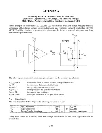
ADP3120ADual Bootstrapped, 12 VMOSFET Driver with OutputDisableThe ADP3120A is a single Phase 12 V MOSFET gate driversoptimized to drive the gates of both high side and low side powerMOSFETs in a synchronous buck converter. The high side andlow side driver is capable of driving a 3000 pF load with a 45 nspropagation delay and a 25 ns transition time.With a wide operating voltage range, high or low side MOSFETgate drive voltage can be optimized for the best efficiency. Internaladaptive nonoverlap circuitry further reduces switching losses bypreventing simultaneous conduction of both MOSFETs.The floating top driver design can accommodate VBST voltages ashigh as 35 V, with transient voltages as high as 40 V. Both gate outputscan be driven low by applying a low logic level to the Output Disable(OD) pin. An Undervoltage Lockout function ensures that both driveroutputs are low when the supply voltage is low, and a ThermalShutdown function provides the IC with overtemperature protection.www.onsemi.comMARKINGDIAGRAMS8811 All In One Synchronous Buck DriverBootstrapped High Side DriveOne PWM Signal Generates Both DrivesAnticross Conduction Protection CircuitryOD for Disabling the Driver Outputs Meets CPU VR Requirementwhen Used with Patented FlexModet ControllerThese are Pb Free Devices1ALYWG8L3CALYWGG Assembly Location Wafer Lot Year Work Week Pb Free PackagePIN 1 Multiphase Desktop CPU Supplies Single Supply Synchronous Buck Converters1DFN8MN SUFFIXCASE 506BJFeatures 3120AALYWGSO 8D SUFFIXCASE 7518BSTINDRVHSWNODPGNDVCCDRVL(Top View)ORDERING INFORMATIONDevicePackageShipping†ADP3120AJRZSO 8(Pb Free)98 Units / RailADP3120AJRZ RLSO 8(Pb Free)2500 / Tape &ReelADP3120AJCPZ RLDFN8(Pb Free)3000 / Tape &Reel†For information on tape and reel specifications,including part orientation and tape sizes, pleaserefer to our Tape and Reel Packaging SpecificationBrochure, BRD8011/D. Semiconductor Components Industries, LLC, 2012August, 2018 Rev. 51Publication Order Number:ADP3120A/D
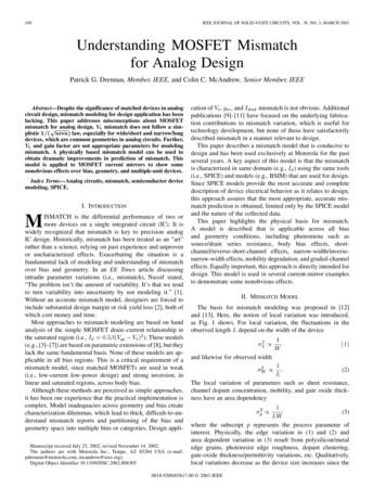
ONITORNON OVERLAPTIMERSMIN DRVLOFF TIMERFigure 1. Block DiagramPIN DESCRIPTIONSO 8DFN8SymbolDescription11BSTUpper MOSFET Floating Bootstrap Supply. A capacitor connected between BST and SW pins holdsthis bootstrap voltage for the high side MOSFET as it is switched. The recommended capacitor valueis between 100 nF and 1.0 mF. An external diode is required with the ADP3120A.22INLogic Level Input. This pin has primary control of the drive outputs.33ODOutput Disable. When low, normal operation is disabled forcing DRVH and DRVL low.44VCCInput Supply. A 1.0 mF ceramic capacitor should be connected from this pin to PGND.55DRVLOutput drive for the lower MOSFET.66PGNDPower Ground. Should be closely connected to the source of the lower MOSFET.77SWNSwitch Node. Connect to the source of the upper MOSFET.88DRVHOutput drive for the upper MOSFET.www.onsemi.com2
ADP3120AMAXIMUM RATINGSRatingValueUnitOperating Ambient Temperature, TA 20 to 85 COperating Junction Temperature, TJ (Note 1) 20 to 150 C45123 C/W C/W7.555 C/W C/W 65 to 150 C260 peak C1 Package Thermal Resistance: SO 8Junction to Case, RqJCJunction to Ambient, RqJA (2 Layer Board)Package Thermal Resistance: DFN8 (Note 2)Junction to Case, RqJC (From die to exposed pad)Junction to Ambient, RqJAStorage Temperature Range, TSLead Temperature Soldering (10 sec): Reflow (SMD styles only)Pb Free (Note 3)JEDEC Moisture Sensitivity LevelSO 8 (260 peak profile)Stresses exceeding those listed in the Maximum Ratings t . N SOURCE2. N GATE3. P SOURCE4. P GATE5. P DRAIN6. P DRAIN7. N DRAIN8. N DRAINSTYLE 15:PIN 1. ANODE 12. ANODE 13. ANODE 14. ANODE 15. CATHODE, COMMON6. CATHODE, COMMON7. CATHODE, COMMON8. CATHODE, COMMONSTYLE 16:PIN 1. EMITTER, DIE #12. BASE, DIE #13. EMITTER, DIE #24. BASE, DIE #25. COLLECTOR, DIE #26. COLLECTOR, DIE #27. COLLECTOR, DIE #18. COLLECTOR, DIE #1STYLE 17:PIN 1. VCC2. V2OUT3. V1OUT4. TXE5. RXE6. VEE7. GND8. ACCSTYLE 18:PIN 1. ANODE2. ANODE3. SOURCE4. GATE5. DRAIN6. DRAIN7. CATHODE8. CATHODESTYLE 19:PIN 1. SOURCE 12. GATE 13. SOURCE 24. GATE 25. DRAIN 26. MIRROR 27. DRAIN 18. MIRROR 1STYLE 20:PIN 1. SOURCE (N)2. GATE (N)3. SOURCE (P)4. GATE (P)5. DRAIN6. DRAIN7. DRAIN8. DRAINSTYLE 21:PIN 1. CATHODE 12. CATHODE 23. CATHODE 34. CATHODE 45. CATHODE 56. COMMON ANODE7. COMMON ANODE8. CATHODE 6STYLE 22:PIN 1. I/O LINE 12. COMMON CATHODE/VCC3. COMMON CATHODE/VCC4. I/O LINE 35. COMMON ANODE/GND6. I/O LINE 47. I/O LINE 58. COMMON ANODE/GNDSTYLE 23:PIN 1. LINE 1 IN2. COMMON ANODE/GND3. COMMON ANODE/GND4. LINE 2 IN5. LINE 2 OUT6. COMMON ANODE/GND7. COMMON ANODE/GND8. LINE 1 OUTSTYLE 24:PIN 1. BASE2. EMITTER3. COLLECTOR/ANODE4. COLLECTOR/ANODE5. CATHODE6. CATHODE7. COLLECTOR/ANODE8. COLLECTOR/ANODESTYLE 25:PIN 1. VIN2. N/C3. REXT4. GND5. IOUT6. IOUT7. IOUT8. IOUTSTYLE 26:PIN 1. GND2. dv/dt3. ENABLE4. ILIMIT5. SOURCE6. SOURCE7. SOURCE8. VCCSTYLE 29:PIN 1. BASE, DIE #12. EMITTER, #13. BASE, #24. EMITTER, #25. COLLECTOR, #26. COLLECTOR, #27. COLLECTOR, #18. COLLECTOR, #1STYLE 30:PIN 1. DRAIN 12. DRAIN 13. GATE 24. SOURCE 25. SOURCE 1/DRAIN 26. SOURCE 1/DRAIN 27. SOURCE 1/DRAIN 28. GATE 1DOCUMENT NUMBER:DESCRIPTION:98ASB42564BSOIC 8 NBSTYLE 27:PIN 1. ILIMIT2. OVLO3. UVLO4. INPUT 5. SOURCE6. SOURCE7. SOURCE8. DRAINSTYLE 28:PIN 1. SW TO GND2. DASIC OFF3. DASIC SW DET4. GND5. V MON6. VBULK7. VBULK8. VINElectronic versions are uncontrolled except when accessed directly from the Document Repository.Printed versions are uncontrolled except when stamped “CONTROLLED COPY” in red.PAGE 2 OF 2onsemi andare trademarks of Semiconductor Components Industries, LLC dba onsemi or its subsidiaries in the United States and/or other countries. onsemi reservesthe right to make changes without further notice to any products herein. onsemi makes no warranty, representation or guarantee regarding the suitability of its products for any particularpurpose, nor does onsemi assume any liability arising out of the application or use of any product or circuit, and specifically disclaims any and all liability, including without limitationspecial, consequential or incidental damages. onsemi does not convey any license under its patent rights nor the rights of others. Semiconductor Components Industries, LLC, 2019www.onsemi.com
onsemi,, and other names, marks, and brands are registered and/or common law trademarks of Semiconductor Components Industries, LLC dba “onsemi” or its affiliatesand/or subsidiaries in the United States and/or other countries. onsemi owns the rights to a number of patents, trademarks, copyrights, trade secrets, and other intellectual property.A listing of onsemi’s product/patent coverage may be accessed at www.onsemi.com/site/pdf/Patent Marking.pdf. onsemi reserves the right to make changes at any time to anyproducts or information herein, without notice. The information herein is provided “as is” and onsemi makes no warranty, representation or guarantee regarding the accuracy of theinformation, product features, availability, functionality, or suitability of its products for any particular purpose, nor does onsemi assume any liability arising out of the application or useof any product or circuit, and specifically disclaims any and all liability, including without limitation special, consequential or incidental damages. Buyer is responsible for its productsand applications using onsemi products, including compliance with all laws, regulations and safety requirements or standards, regardless of any support or applications informationprovided by onsemi. “Typical” parameters which may be provided in onsemi data sheets and/or specifications can and do vary in different applications and actual performance mayvary over time. All operating parameters, including “Typicals” must be validated for each customer application by customer’s technical experts. onsemi does not convey any licenseunder any of its intellectual property rights nor the rights of others. onsemi products are not designed, intended, or authorized for use as a critical component in life support systemsor any FDA Class 3 medical devices or medical devices with a same or similar classification in a foreign jurisdiction or any devices intended for implantation in the human body. ShouldBuyer purchase or use onsemi products for any such unintended or unauthorized application, Buyer shall indemnify and hold onsemi and its officers, employees, subsidiaries, affiliates,and distributors harmless against all claims, costs, damages, and expenses, and reasonable attorney fees arising out of, directly or indirectly, any claim of personal injury or deathassociated with such unintended or unauthorized use, even if such claim alleges that onsemi was negligent regarding the design or manufacture of the part. onsemi is an EqualOpportunity/Affirmative Action Employer. This literature is subject to all applicable copyright laws and is not for resale in any manner.PUBLICATION ORDERING INFORMATIONLITERATURE FULFILLMENT:Email Requests to: orderlit@onsemi.comonsemi Website: www.onsemi.com TECHNICAL SUPPORTNorth American Technical Support:Voice Mail: 1 800 282 9855 Toll Free USA/CanadaPhone: 011 421 33 790 2910Europe, Middle East and Africa Technical Support:Phone: 00421 33 790 2910For additional information, please contact your local Sales Representative
MOSFET Driver with Output Disable The ADP3120A is a single Phase 12 V MOSFET gate drivers optimized to drive the gates of both high side and low side power MOSFETs in a synchronous buck converter. The high side and low side driver is capable of driving a 3000 pF load with a 45 ns propagation delay and a 25 ns transition time.