Transcription
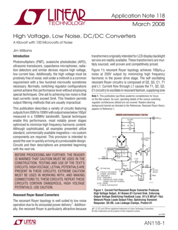
Application Note 118March 2008High Voltage, Low Noise, DC/DC ConvertersA Kilovolt with 100 Microvolts of NoiseJim WilliamsThis publication describes a variety of circuits featuringoutputs from 200V to 1000V with output noise below 100µVmeasured in a 100MHz bandwidth. Special techniquesenable this performance, most notably power stagesoptimized to minimize high frequency harmonic content.Although sophisticated, all examples presented utilizestandard, commercially available magnetics—no customcomponents are required. This provision is intended toassist the user in quickly arriving at a produceable design.Circuits and their descriptions are presented beginningwith the next ink.BEFORE PROCEEDING ANY FURTHER, THE READERIS WARNED THAT CAUTION MUST BE USED IN THECONSTRUCTION, TESTING AND USE OF THE TEXT’SCIRCUITS. HIGH VOLTAGE, LETHAL POTENTIALS AREPRESENT IN THESE CIRCUITS. EXTREME CAUTIONMUST BE USED IN WORKING WITH, AND MAKINGCONNECTIONS TO, THESE CIRCUITS. REPEAT: THESECIRCUITS CONTAIN DANGEROUS, HIGH VOLTAGEPOTENTIALS. USE CAUTION.Resonant Royer Based ConvertersThe resonant Royer topology is well suited to low noiseoperation due to its sinosoidal power delivery1. Additionally, the resonant Royer is particularly attractive becauseFigure 1’s resonant Royer topology achieves 100µVP-Pnoise at 250V output by minimizing high frequencyharmonic in the power drive stage. The self oscillatingresonant Royer circuitry is composed of Q2, Q3, C1, T1and L1. Current flow through L1 causes the T1, Q2, Q3,C1 circuitry to oscillate in resonant fashion, supplying sineNote 1. This publication sacrifices academic completeness for focuson the title subject. As such, operating details of the various switchingregulator architectures utilized are not covered. Readers desiringbackground tutorial are directed to the References. Resonant Royer theoryappears in Reference 1.DANGER! Lethal Potentials Present — See Text250VOUT1µF, 400V10k1µF, �FC15Vx23D5Q2Q3L1250µH ZDT1048 DUALIRLRO24Q1L1 CTX250-4, COILTRONICST1 210605R, COILTRONICS1µF WIMA MKS-40.22µF WIMA MKP-2D1-D4 TOSHIBA DUAL DIODE 1SS306.CONNECT EACH UNIT IN SERIES.D5-D6 2N4393* 1% METAL FILM RESISTOR10kD60.1µF430kLT1635VREF 0.2V Photomultipliers (PMT), avalanche photodiodes (APD),ultrasonic transducers, capacitance microphones, radiation detectors and similar devices require high voltage,low current bias. Additionally, the high voltage must bepristinely free of noise; well under a millivolt is a commonrequirement with a few hundred microvolts sometimesnecessary. Normally, switching regulator configurationscannot achieve this performance level without employingspecial techniques. One aid to achieving low noise is thatload currents rarely exceed 5mA. This freedom permitsoutput filtering methods that are usually impractical.transformers originally intended for LCD display backlightservice are readily available. These transformers are multiply sourced, well proven and competitively N118 F01Figure 1. Current Fed Resonant Royer Converter ProducesHigh Voltage Output. A1 Biases Q1 Current Sink, EnforcingOutput Voltage Stabilizing Feedback Loop. A1’s 0.001µF–1kΩNetwork Phase Leads Output Filter, Optimizing TransientResponse. D5-D6, Low Leakage Clamps, Protect A1L, LT, LTC and LTM are registered trademarks of Linear Technology Corporation.All other trademarks are the property of their respective owners.an118fbAN118-1
Application Note 118wave drive to T1’s primary with resultant sine-like highvoltage appearing across the secondary.The circuit’s low harmonic content combined with theRC output filter produces a transcendently clean output.Output noise (Figure 3) is just discernible in the monitoringinstrumentation’s 100µV noise floor3.T1’s rectified and filtered output is fed back to amplifierreference A1 which biases the Q1 current sink, completinga control loop around the Royer converter. L1 ensuresthat Q1 maintains constant current at high frequency.Milliampere level output current allows the 10k resistorin the output filter. This greatly aids filter performancewith minimal power loss.2 The RC path to A1’s negativeinput combines with the 0.1µF capacitor to compensateA1’s loop. D5 and D6, low leakage clamps, protect A1during start-up and transient events. Although Figure2’s collector waveforms are distorted, no high frequencycontent is present.Figure 4’s variant of Figure 1 maintains 100µV output noisewhile extending input supply range to 32V. Q1 may requireheat sinking at high input supply voltage. Converter andloop operation is as before although compensation components are re-established to accommodate the LT1431control element.Note 2. As previously mentioned, low current requirements permit certainfreedoms in the output filter and feedback network. See Appendix A forexamples and discussion.Note 3. Measurement technique and instrumentation choice for faithfullow level noise measurement requires diligence. See Appendices Bthrough E for practical considerations.DANGER! Lethal Potentials Present — See Text250VOUT1µF, 400VA 5V/DIV10k 1µF, 400VB 5V/DIV1M*D1-D40.001µF400V20µs/DIV10AN118 F026T1Figure 2. Resonant Royer Collector Waveforms Are DistortedSinosoids; No High Frequency Content is RLRO24Q1 ZDT1048 DUAL100µV/DIVAC COUPLED1k10kOUT0.2µFL1 CTX250-4, COILTRONICST1 210605R, COILTRONICS1µF WIMA MKS-40.22µF WIMA MKP-2D1-D4 TOSHIBA DUAL DIODE 1SS306.CONNECT EACH UNIT IN SERIES.D5-D6 1N4148* 1% METAL FILM RESISTOR10µs/DIV VLT1431COMPFBGND GND5kOUTPUTADJUST7.5k*AN118 F04AN118 F03Figure 3. Figure 1’s Output Noise is Just Discernable inMonitoring Instrumentation’s 100µV Noise FloorFigure 4. LT1431 Regulator Based Variant of Figure 1 Maintains100µV Output Noise While Extending Input Supply Range to 32V.Q1 May Require Heat Sinking at High Input Supply Voltagesan118fbAN118-2
Application Note 118DANGER! Lethal Potentials Present — See Text250VOUT1µF, 400V ZDT1048 DUALThe previous resonant Royer examples utilize linear control of converter current to furnish harmonic free drive.The trade off is decreased efficiency, particularly as inputvoltage scales. Improved efficiency is possible by employing switched mode current drive to the Royer converter.Unfortunately, such switched drive usually introducesnoise. As will be shown, this undesirable consequencecan be countered.10kL1 CTX250-4, COILTRONICST1 210605R, COILTRONICS1µF WIMA MKS-40.22µF WIMA MKP-2D1-D4 TOSHIBA DUAL DIODE1SS306. CONNECT EACHUNIT IN SERIES.D5-D6 1N4148* 1% METAL FILM RESISTOR1µF, 11MFB2.5kOUTPUTADJUSTMODERTVC20kSwitched Current Source Based Resonant RoyerConverters3.65k*1µFFigure 5 replaces the linearly operated current sink with aswitching regulator. The Royer converter and its loop are asbefore; Figure 6’s transistor collector waveshape (trace A)is similar to the other circuits. The high speed, switchmode current sink drive (trace B) efficiently feeds L1. Thisswitched operation improves efficiency but degrades outputnoise. Figure 7 shows switching regulator harmonic clearlyresponsible for 3mV peak to peak output noise – about 30times greater than the linearly operated circuits.Careful examination of Figure 7 reveals almost no Royerbased residue. The noise is dominated by switchingregulator artifacts. Eliminating this switching regulatororiginated noise while maintaining efficiency requiresspecial circuitry but is readily achievable.AN118 F05Figure 5. Replacing Linearly Operated Current Sink withSwitching Regulator Minimizes Heating Although Output NoiseIncreasesA 5V/DIVA 1mV/DIVAC COUPLEDB 5V/DIVA 20µs/DIVB 1µs/DIV(TRIGGERS ASYNCRONOUS)AN118 F06Figure 6. Resonant Royer Collector Waveshape (Trace A) isSimilar to Previous Circuits. High Speed, Switched Mode CurrentSink Drive (Trace B) Efficiency Feeds L1500ns/DIVAN118 F07Figure 7. Switching Regulator HarmonicResults in 3mVP-P Output Noisean118fbAN118-3
Application Note 118Low Noise Switching Regulator Driven ResonantRoyer ConvertersFigure 8 examplifies the aforementioned “special circuitry”.The resonant Royer converter and its loop are reminiscent of previous circuits. The fundamental difference isthe LT1534 switching regulator which utilizes controlledtransition times to retard high frequency harmonic whilemaintaining efficiency. This approach blends switching andlinear current sink benefits4. Voltage and current transition rate, set by RV and RI respectively, is a compromisebetween efficiency and noise reduction.Figure 9’s Royer collector waveshape (trace A) is nearlyidentical to the one produced by Figure 5’s circuit. TraceB, depicting LT1534 controlled transition times, markedlydeparts from its Figure 5 counterpart. These controlledtransition times dramatically reduce output noise (Figure10) to 150µVP-P — a 20x improvement vs Figure 7’sLTC3401 based results.Note 4. As stated, this forum must suffer brevity to maintain focus. TheLT1534’s controlled transition time operation mandates further study. SeeReference 3.DANGER! Lethal Potentials Present — See Text250VOUT1µF, 400V ZDT1048 DUALL2 COILCRAFT B08TL1 CTX250-4, COILTRONICST1 210605R, COILTRONICS1µF WIMA MKS-40.22µF WIMA MKP-2D1-D4 TOSHIBA DUAL DIODE1SS306. CONNECT EACHUNIT IN SERIES.D5-D6 1N4148* 1% METAL FILM RESISTOR1kB 5V/DIV1µF, 400V1M*0.002µF400VD1-D410A 20µs/DIVB 10µs/DIV(TRIGGERS ADJUSTL11N5817AN118 F09Figure 9. Resonant Royer Collector Waveshape(Trace A) is Identical to Figure 5’s LT3401 Circuit;LT1534 Current Sink’s Controlled Transition Times(Trace B) Attenuate High Frequency HarmonicT15A 5V/DIV4.53k*CT V820pFCOLFBA 100µV/DIVAC COUPLEDLT1534RT16.9k*GND VCPGND0.1µFL228nHRV33kRI33kAN118 F08Figure 8. LT1534’s Controlled Transition Times Retard HighFrequency Harmonic and Maintain Low Heat Dissipation.Approach Blends Switching and Linear Current Sink Benefits10µs/DIVAN118 F10Figure 10. Switched Current Sinks Controlled TransitionTimes Dramatically Lower Noise to 150µVP-P —A 20xImprovement vs Figure 7’s LTC3401 Resultsan118fbAN118-4
Application Note 118Figure 11 is essentially identical to Figure 8 except thatit produces a negative 1000V output. A1 provides lowimpedance, inverting feedback to the LT1534. Figure 12a’soutput noise measures inside 1mV. As before, resonantRoyer ripple dominates the noise — no high frequencycontent is detectable. It is worth noting that this noisefigure proportionally improves with increased filter capacitor values. For example, Figure 12b indicates only100µV noise with filter capacitor values increased by 10x,although capacitor physical size is large. The original values selected represent a reasonable compromise betweennoise performance and physical size.–1000VOUT0.015µF, 2kVDANGER! Lethal Potentials Present — See Text10k0.033µF, 2k9M**D1-D4106T1510.22µF820Ω35V5kOUTPUTADJUST ZDT1048 DUALCT8.06k*1N5817 V820pFCOLFBLT1006R1 5VL1 CTX150-4, COILTRONICST1 210609R, COILTRONICS0.033µF/0.015µF WIMA MKS-40.22µF WIMA MKP-2D1-D4 1N6529L2 COILCRAFT B08TD5-D6 1N4148* 1% METAL FILM RESISTOR** IRC, CGH-1, 1%2–5V4LT1534RT16.9k*GND VC PGND15µFL228nHRV24kRI39kAN118 F11Figure 11. Controlled Transition Time Switching Regulator Applied to a Negative Output,1000V Converter. A1 Provides Low Impedance, Inverting Feedback to LT1534A 100µV/DIVAC COUPLEDA 500µV/DIVAC COUPLED10µs/DIVAN118 F12aFigure 12a. –1000V Converter Output Noise MeasuresInside 1mV (1PPM-0.0001%) in 100MHz Bandwidth.Resonant Royer Related Ripple Dominates Residue—No High Frequency Content is Detectable10µs/DIVAN118 F12bFigure 12b. 10x Increase in Figure 11’s Filter Capacitor ValuesReduces Noise to 100µV. Penalty is Capacitor Physical Sizean118fbAN118-5
Application Note 118Controlled Transition Push-Pull ConvertersControlled transition techniques are also directly applicableto push-pull architectures. Figure 13 uses a controlledtransition push-pull regulator in a simple loop to controla 300V output converter. Symmetrical transformer driveand controlled switching edge times promote low outputnoise. The D1-D4 connected damper further minimizesresidual aberrations. In this case, inductors are used inthe output filter although appropriate resistor values couldbe employed.Figure 14 displays smooth transitions at the transformersecondary outputs (trace A is T1 Pin 4, trace B, T1 Pin 7).Absence of high frequency harmonic results in extremelylow noise. Figure 15’s fundamental related output residue approaches the 100µV measurement noise floor ina 100MHz bandpass. This is spectacularly low noiseperformance in any DC/DC converter and certainly inone providing high voltage. Here, at 300V output, noiserepresents less than 1 part in 3 million.Figure 16 is similar except that output range is variablefrom 0V to 300V. The LT1533 is replaced by an LT3439which contains no control elements. It simply drives thetransformer with 50% duty cycle, controlled switchingtransitions. Feedback control is enforced by A1-Q1-Q2driving current into T1’s primary center tap. A1 comparesa resistively derived portion of the output with a user supplied control voltage. The values shown produce a 0V to300V output in response to a 0V to 1V control voltage. AnRC network from Q2’s collector to A1’s positive input compensates the loop. Collector waveforms and output noisesignature are nearly identical to Figure 13. Output noise is100µVP-P over the entire 0V to 300V output range.DANGER! Lethal Potentials Present — See Text0.01µFL1330µH150ΩL2330µH300VOUT 10µF450VD1-D4A 200V/DIV 4.7µF450VB 200V/DIV47 (TIE 5-6)1M*T115V680pF V25VCOLA3COLBCT16.9k*2µs/DIVFigure 14. Transformer Secondary OutputsShow No High Frequency ArtifactsFB1kOUTPUT ADJUSTLT1533RT3.83k*0.1µFVCAN118 F14GND PGNDL328nHRV33kRI43kAN118 F13* 1% METAL FILM RESISTORL3 COILCRAFT B08TL1, L2 COILCRAFT LPS5010-334MLBD1-D4 1N6529T1 PICO 32195Figure 13. A Push-Pull Drive, Controlled Transition,300V Output Converter. Symmetrical TransformerDrive and Slow Edges Promote Low Output NoiseA 100µV/DIVAC COUPLED5µs/DIVAN118 F15Figure 15. Push-Pull Converter Related Residue Approaches100µV Measurement Noise Floor. No Wideband ComponentsAppear in 100MHz Measurement Bandpassan118fbAN118-6
Application Note 118Flyback Convertersvoltage stress. Q1, operating as a “cascode” with theLT1172’s internal switch, withstands L1’s high voltageflyback events6.Flyback converters, due to their abrupt, poorly controlledenergy delivery, are not usually associated with low noiseoutput. However, careful magnetic selection and layoutcan provide surprisingly good performance, particularlyat low output current.Diodes associated with Q1’s source terminal clamp L1originated spikes arriving via Q1’s junction capacitance. Thehigh voltage is rectified and filtered, forming the circuits’output. The ferrite bead, 100Ω and 300Ω resistors aid filterFigure 17’s design provides 200V from a 5V input5. Thescheme is a basic inductor flyback boost regulator withsome important deviations. Q1, a high voltage device, hasbeen interposed between the LT1172 switching regulatorand the inductor. This permits the regulator to controlQ1’s high voltage switching without undergoing high0.01µFNote 5. LTC application note veterans, a weary crew, will recognizematerial in this section from AN98 and AN113. The original circuits andtext have been modified as necessary to suit low noise operation. SeeReferences.Note 6. See References 13-17 for historical perspective and study oncascodes.L1330µH150Ω 10µF400V1µFDANGER! Lethal Potentials Present — See Text4T17 (TIE µF510k5V100Ω680pFCOLACT16.9k*100kLTC6240D44Q23 A15V* 1% METAL FILM RESISTORT1 PICO 321955VD1-D4 1N6529L1 COILCRAFT LP5010-334MLBVOUT0 TO 300V4.7µF400VCOLB510kLT3439RT VGNDRSL27kVCONTROL0 TO 1VPGNDAN118 F16Figure 16. Full Range Adjustable Version of Figure 13. VCONTROL Directed A1 Sets T1 Drive Via Q1-Q2. 1M-3.32k DividerProvides Feedback, Stabilized by A1’s Input Capacitors. Waveforms Are Similar to Figure 13. Output Noise is 100µVP-P5V 1N571233µF100k1µF1N5256B30V 5%15V1N4702Q1IRF8401N5819300ΩOUTPUT200V1µF 2x –0.47µF250V1M*LT1172VINFB1µFVC FERRITE BEAD FERRONICS 21-110J* 1% METAL FILM RESISTORL1 33µH, COILTRONICS UP2B0.47µF PANASONIC ECW-U2474KCVGNDE2BAS5210.47µF250VSW5V DANGER! Lethal Potentials Present — See TextL1BAS521 100ΩE16.19k*1k AN118 F171µFFigure 17. 5V to 200V Output Converter. Cascoded Q1 Switches High Voltage, Allowing Low Voltage Regulator to Control Output. DiodeClamps Protect Regulator from Transients; 100k Path Bootstraps Q1’s Gate Drive from L1’s Flyback Events. Output Connected 300ΩDiode Combination Provides Short-Circuit Protection. Ferrite Bead, 100Ω and 300Ω Resistors Minimize High Frequency Output Noisean118fbAN118-7
Application Note 118efficiency7. Feedback to the regulator stabilizes the loopand the VC pin network provides frequency compensation.A 100k path from L1 bootstraps Q1’s gate drive to about10V, ensuring saturation. The output connected diodeprovides short-circuit protection by shutting down theLT1172 if the output is accidentally grounded.Figure 18’s traces A and C are LT1172 switch current andvoltage, respectively. Q1’s drain is trace B. Current ramptermination results in a high voltage flyback event at Q1’sdrain. A safely attenuated version of the flyback appearsat the LT1172 switch. The sinosoidal signature, due toinductor ring-off between conduction cycles, is harmless.Figure 19, output noise, is composed of low frequencyripple and wideband, flyback related spikes measuring1mVP-P in a 100MHz bandpass.Figure 20, contributed by Albert M. Wu of LTC, is a transformer coupled flyback circuit. The transformer secondaryprovides voltage step-up referred to the flyback drivenprimary. The 4.22M resistor supplies feedback to the regulator, closing a control loop. A 10k-0.68µF filter networkattenuates high frequency harmonic with minimal voltagedrop. Flyback related transients are clearly visible in Figure21’s output noise although within 300µVP-P.Note 7. Tutorial on ferrite beads appears in Appendix F.DANGER! Lethal Potentials Present — See TextT11:10:4VIN5V7, 8D14.7µHA 0.5A/DIV5, 6VIN4SYNC SSC 20V/DIV464k2µs/DIVAN118 F18VOUT 80RTFBB 100V/DIV10k1RFB 4.22M*VC10k0.47µF10nF100pFAN118 F20Figure 18. Waveforms for 5V to 200V Converter Include LT1172Switch Current and Voltage (Traces A and C, Respectively) andQ1’s Drain Voltage (Trace B). Current Ramp Termination Resultsin High Voltage Flyback Event at Q1 Drain. Safely AttenuatedVersion Appears at LT1172 Switch. Sinosoidal Signature,Due to Inductor Ring-Off Between Current Conduction Cycles,is Harmless. All Traces Intensified Near Center Screen forPhotographic ClarityC1: 2.2µF, 25V, X5R, 1206C2: TDK C3225X7R2J683MD1: VISHAY GSD2004S DUAL DIODE CONNECTED IN SERIEST1: TDK LDT565630T-041C3: WIMA MKS-4* IRC-CGH-1, 1%Figure 20. 5V Powered Transformer CoupledFlyback Converter Produces 350V OutputA 200µV/DIVAC COUPLED1mV/DIVAC COUPLED5µs/DIVAN118 F19Figure 19. Figure 17’s Output Noise, Composed of LowFrequency Ripple and Wideband, Flyback RelatedSpikes, Measures 1mVP-P in 100MHz Bandpass2µs/DIVAN118 F21Figure 21. High Speed Transients in Figure 20’sNoise Signature are Within 300µVP-Pan118fbAN118-8
Application Note 118Figure 24’s post-regulator reduces Figure 22’s outputripple and noise to only 2mV. A1 and the LT3468 areidentical to the previous circuit, except for the 15V zenerdiode in series with the 10M-100k feedback divider. Thiscomponent causes C1’s voltage, and hence Q1’s collector,to regulate 15V above the VPROGRAM input dictated point.The VPROGRAM input is also routed to the A2-Q2-Q1 linearpost-regulator. A2’s 10M-100k feedback divider does notinclude a zener, so the post-regulator follows the VPROGRAMinput with no offset. This arrangement forces 15V acrossQ1 at all output voltages. This figure is high enough toeliminate undesirable ripple and noise from the outputwhile keeping Q1 dissipation low.54.7µFT18VIN C113µF330V0V TO 300VOUT5mA MAXIMUM1SWLT3468CHARGED14D2GND10M*DONEA1LT100633pF Figure 23’s 250V DC output (Trace B) decays down about2V until A1 (Trace A) goes high, enabling the LT3468 andrestoring the loop. This simple circuit works well, regulating over a programmable 0V to 300V range, although itsinherent hysteretic operation mandates the (unacceptable)2V output ripple noted. Loop repetition rate varies withinput voltage, output set point and load but the ripple isalways present. The following circuit greatly reduces rippleamplitude although complexity increases.5V–Figure 22 employs the LT3468 photoflash capacitor chargeras a general purpose high voltage DC/DC converter. Normally, the LT3468 regulates its output at 300V by sensingT1’s flyback pulse characteristic. This circuit allows theLT3468 to regulate at lower voltages by truncating itscharge cycle before the output reaches 300V. A1 comparesa divided down portion of the output with the programinput voltage. When the program voltage (A1 input) isexceeded by the output derived potential (A1 – input) A1’soutput goes low, shutting down the LT3468. The feedbackcapacitor provides AC hysteresis, sharpening A1’s outputto prevent chattering at the trip point. The LT3468 remainsshut down until the output voltage drops low enough to tripA1’s output high, turning it back on. In this way, A1 dutycycle modulates the LT3468, causing the output voltageto stabilize at a point determined by the program input.100k*10k10kVPROGRAM INPUT0V TO 3V 0V TO 300VOUT*1% METAL FILM RESISTORC1: RUBYCON 330FW13AK6325AN118 F22D1: TOSHIBA DUAL DIODE 1SS306,CONNECT DIODES IN SERIESD2: PANASONIC MA2Z720T1: TDK LDT565630T-002Figure 22. A Voltage Programmable 0V to 300V OutputRegulator. A1 Controls Regulator Output by Duty CycleModulating LT3468/T1 DC/DC Converter Power DeliveryA 5V/DIVA 1V/DIVAC COUPLEDON 250V DCLEVEL20ms/DIVAN118 F23Figure 23. Details of Figure 22’s Duty Cycle ModulatedOperation. High Voltage Output (Trace B) Ramps DownUntil A1 (Trace A) Goes High, Enabling LT3468/T1 toRestore Output. Loop Repetition Rate Varies with InputVoltage, Output Set Point and LoadQ3 and Q4 form a current limit, protecting Q1 from overload.Excessive current through the 50Ω shunt turns Q3 on. Q3drives Q4, shutting down the LT3468. Simultaneously, aportion of Q3’s collector current turns Q2 on hard, shuttingoff Q1. This loop dominates the normal regulation feedback,protecting the circuit until the overload is removed.an118fbAN118-9
Application Note 118DANGER! Lethal Potentials Present — See TextQ3D15V54.7µFT1Q148 1C113µF330V200k1N470215VLT3468 GNDCHARGEDONE†0.01µF0V TO 300VOUT5mA MAXIMUM10M*10k 10kQ2D2SW1kD30.68µF†VIN10k50Ω1kA21/2 LT10130.1µF100k**–10M*100k5VA11/2 LT101333pF Q42N3904–10k100k**10k10k100k10kAN118 F24*1% METAL FILM RESISTOR**0.1% METAL FILM RESISTOR†WIMA MKS-4, 400VC1: RUBYCON 330FW13AK6325D1: TOSHIBA DUAL DIODE 1SS306,CONNECT DIODES IN SERIESD2: PANASONIC MA2Z720D3: 1N4148Q1, Q2: 2N6517Q3: 2N6520T1: TDK LDT565630T-002VPROGRAM INPUT0V TO 3V 0V TO 300VOUTFigure 24. Post-Regulation Reduces Figure 22’s 2V Output Ripple to 2mV. LT3468-Based DC/DC Converter, Similarto Figure 22, Delivers High Voltage to Q1 Collector. A2, Q1, Q2 Form Tracking, High Voltage Linear Regulator.Zener Sets Q1 VCE 15V, Ensuring Tracking with Minimal Dissipation. Q3-Q4 Limit Short-Circuit Output CurrentFigure 25 shows just how effective the post regulatoris. When A1 (trace A) goes high, Q1’s collector (trace B)ramps up in response (note LT3468 switching artifactson ramps upward slope). When the A1-LT3468 loop issatisfied, A1 goes low and Q1’s collector ramps down.The output post-regulator (trace C), however, rejects theripple, showing only 2mV of noise. Slight trace blurringderives from A1-LT3468 loop jitter.Summary of Circuit CharacteristicsFigure 26 summarizes the circuits presented with salientcharacteristics noted. This chart is only a generalizedguideline and not an indicator of capabilities or limits.There are too many variables and exceptions to accomodate the categorical statement a chart implies. Theinterdependence of circuit parameters makes summarizingor rating various approaches a hazardous exercise. Thereis simply no intellectually responsible way to streamlinethe selection and design process if optimum results aredesired. A meaningful choice must be the outcome oflaboratory-based experimentation. There are just too manyinterdependent variables and surprises for a systematic,AN118-10A 5V/DIVB 0.1V/DIVAC COUPLEDC 5mV/DIVAC COUPLEDON 200V DCLEVEL100µs/DIVAN118 F25Figure 25. Low Ripple Output (Trace C) is Apparent in PostRegulator’s Operation. Traces A and B are A1 Output and Q1’sCollector, Respectively. Trace Blurring, Right of Photo Center,Derives from Loop Jittertheoretically based selection. Charts seek authority throughglib simplification and simplification is Disaster’s deputy.Nonetheless, Figure 26, in all its appropriated glory, listsinput supply range, output voltage and current along withcomments for each circuit8.Note 8. Readers detecting author ambivalence at Figure 26’s inclusion arenot hallucinating. Locally based marketeers champion such charts; thewriter is less enthusiastic.an118fb
Application Note 118FIGURENUMBERSUPPLY RANGE(1mA LOAD)LT1635 - Linear Resonant Royer12.7V to 12V2mA at 250V 100µV Wideband Noise. Easily Voltage Controlled.Potential Dissipation Issue at High Supply Voltages.LT1431 - Linear Resonant Royer42.7V to 32V2mA at 250V 100µV Wideband Noise. Wide Supply Range.Potential Dissipation Issue at High Supply Voltages.LT3401 - Switched Resonant Royer52.7V to 5V3.5mA at 250V3mV Wideband Noise. High Output Current, BetterEfficiency than Figures 1 and 4.LT1534 - Switched Resonant Royer82.7V to 15V2mA at 250V 100µV Wideband Noise. Good Trade-Off BetweenFigures 1, 4 and 5.LT1534 - Swiched Resonant Royer114.5V to 15V1.2mA at –1000VLT1533 Push-Pull132.7V to 15V2mA at 300VLT3439 Push-Pull164.5V to 6V2mA at 0V to 300VCIRCUIT TYPEMAXIMUM OUTPUTCURRENT AT TEST VOLTAGE COMMENTS1mV Wideband Noise Reducable to 100µV. Negative1000V Output Suits Photomultiplier Tubes. 100µV Wideband Noise.Full Range Adjustable Version of Figure 13. 100µVWideband Noise.LT1172 - Cascode Inductor Flyback173.5V to 30V2mA at 200VVOUT Limit 200V. 1mV Wideband Noise.LT3580 - XFMR Flyback202.7V to 20V4mA at 350V300µV Wideband Noise. Wide Supply Range. HighOutput Current. Small Transformer.LT3468 - LT1006 XFMR Flyback223.8V to 12V5mA at 250V1.5V Noise. Simple Voltage Control Input 0VIN to 3VIN 0VOUT – 300VOUT.LT3468 - LT1013 XFMR Flyback- Linear243.8V to 12V5mA at 250V2mV Wideband Noise. Voltage Control Input0VIN to 3VIN 0VOUT to 300VOUT.Figure 26. Summarized Characteristics of Techniques Presented. Applicable Circuit Depends on Application SpecificsNote: This application note was derived from a manuscript originally prepared for publication in EDN magazine.REFERENCES1.Williams, Jim, “A Fourth Generation of LCD BacklightTechnology,” Linear Technology Corporation, Application Note 65, November 1995, p. 32-34, 119.6.Williams, Jim, “Minimizing Switching Residue inLinear Regulator Outputs”. Linear Technology Corporation, Application Note 101, July 2005.2.Bright, Pittman and Royer, “Transistors As On-OffSwitches in Saturable Core Circuits,” Electrical Manufacturing, December 1954. Available from TechnomicPublishing, Lancaster, PA.7.Morrison, Ralph, “Grounding and Shielding Techniques in Instrumentation,” Wiley-Interscience,1986.3.Williams, Jim, “A Monolithic Switching Regulator with100µV Output Noise,” Linear Technology Corporation,Application Note 70, October 1997.8.Fair-Rite Corporation, “Fair-Rite Soft Ferrites,” FairRite Corporation, 1998.9.Sheehan, Dan, “Determine Noise of DC/DC Converters,” Electronic Design, September 27, 1973.4.Baxendall, P.J., “Transistor Sine-Wave LC Oscillators,”British Journal of IEEE, February 1960, Paper No.2978E.5.Williams, Jim, “Low Noise Varactor Biasing withSwitching Regulators,” Linear Technology Corporation, Application Note 85, August 2000, p. 4-6.10. Ott, Henry W., “Noise Reduction Techniques in Electronic Systems,” Wiley Interscience, 1976.11. Tektronix, Inc. “Type 1A7A Differential AmplifierInstruction Manual,” “Check Overall Noise LevelTangentially”, p. 5-36 and 5-37, 1968.an118fbAN118-11
Application Note 11812. Witt, Jeff, “The LT1533 Heralds a New Class of Low NoiseSwitching Regulators,” Linear Technology, Vol. VII, No.3, August 1997, Linear Technology Corporation.16. Williams, Jim, “Signal Sources, Conditioners andPower Circuitry,” Linear Technology Corporation,Application Note 98, November 2004, p. 20-21.13. Williams, Jim, “Bias Voltage and Current Sense Circuitsfor Avalanche Photodiodes,” Linear Technology Corporation, Application Note 92, November 2002, p.8.17. Williams, Jim, “Power Conversion, Measurementand Pulse Circuits,” Linear Technology Corporation,Application Note 113, August 2007.14. Williams, Jim, “Switching Regulators for Poets,” Appendix D, Linear Technology Corporation, ApplicationNote 25, September 1987.18. Williams, Jim and Wu, Albert, “Simple Circuitry forCellular Telephone/Camera Flash Illumination,” LinearTechnology Corporation, Application Note 95, March2004.15. Hickman, R.W. and Hunt, F.V., “On Electronic VoltageStabilizers,” “Cascode,” Review of Scientific Instruments, January 1939, p. 6-21, 16.19. LT3580 Data Sheet, Linear Technology Corporation.APPENDIX AFROM HVRECTIFICEROUTFROM HV RECTIFICERFROM HVRECTIFICERR VINOUT VINTO FBTO FB(a)TO FB(b)FROM HVRECTIFICER ROUTFROM HVRECTIFICEROUT(c)STRAY FLUXC PARASITICROUTFROMHVRECTIFIER VIN VINTO FBLOUTLOSS TERMSTO FBLOSS TERMS(d)(e)(f)AN118 A1Figure A1. Feedback Network Options. (a) Is Basic DC Feedback.
CIRCUITS CONTAIN DANGEROUS, HIGH VOLTAGE POTENTIALS. USE CAUTION. Resonant Royer Based Converters The resonant Royer topology is well suited to low noise operation due to its sinosoidal power delivery 1. Addition-ally, the resonant Royer is particularly attractive because High Voltage, Low Noise, DC/DC Converters A Kilovolt with 100 Microvolts .