Transcription
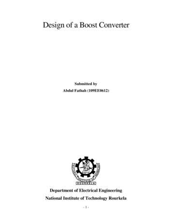
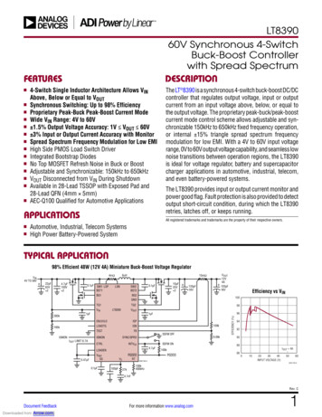
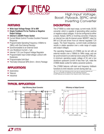
LT3958High Input Voltage,Boost, Flyback, SEPIC andInverting ConverterDESCRIPTIONFEATURESnnnnnnnnnnnWide Input Voltage Range: 5V to 80VSingle Feedback Pin for Positive or NegativeOutput VoltageInternal 3.3A/84V Power SwitchCurrent Mode Control Provides Excellent TransientResponseProgrammable Operating Frequency (100kHz to1MHz) with One External ResistorSynchronizeable to an External ClockLow Shutdown Current 1μAInternal 7.2V Low Dropout Voltage RegulatorProgrammable Input Undervoltage Lockout withHysteresisProgrammable Soft-StartThermally Enhanced QFN (5mm 6mm) PackageThe LT 3958 is a wide input range, current mode, DC/DCconverter which is capable of generating either positiveor negative output voltages. It can be configured as eithera boost, flyback, SEPIC or inverting converter. It featuresan internal low side N-channel power MOSFET rated for84V at 3.3A and driven from an internal regulated 7.2Vsupply. The fixed frequency, current-mode architectureresults in stable operation over a wide range of supplyand output voltages.The operating frequency of LT3958 can be set with anexternal resistor over a 100kHz to 1MHz range, and canbe synchronized to an external clock using the SYNC pin.A minimum operating supply voltage of 5V, and a lowshutdown quiescent current of less than 1μA, make theLT3958 ideally suited for battery-powered systems.The LT3958 features soft-start and frequency foldbackfunctions to limit inductor current during lL, LT, LTC, LTM, Linear Technology and the Linear logo are registered trademarks andNo RSENSE and ThinSOT are trademarks of Linear Technology Corporation.All other trademarks are the property of their respective owners. Patents pending.TYPICAL APPLICATIONHigh Efficiency Boost ConverterEfficiency vs Output CurrentVIN12V TO DSENSE1SYNCSENSE2464kVOUT48V0.5A100VIN 24V95EFFICIENCY 15.8k4.7μF7570010nF400100200300OUTPUT CURRENT (mA)5003958 TA01b3958 TA01a3958f1
LT3958ABSOLUTE MAXIMUM RATINGSPIN CONFIGURATION(Note 1)VCFBXSSRTSYNCNCNCTOP VIEW36 35 34 33 32 31 30NC 128 INTVCC27 VINNC 2SENSE2 337SGNDSGND 425 EN/UVLO24 SGND23 SGNDSENSE1 638SWSW 8SW 921 SW20 SWNC 10GNDGNDGNDGNDGND12 13 14 15 16 17GNDVIN, EN/UVLO (Note 5) .80VSW .84VINTVCC . VIN 0.3V, 15VSYNC .8VVC, SS.3VRT . 1.5VSENSE1, SGND . Internally Connected to GNDSENSE2. 0.3VFBX . –6V to 6VOperating Temperature Range(Note 2) . –40 C to 125 CMaximum Junction Temperature. 125 CStorage Temperature Range. –65 C to 125 CUHE PACKAGE36-LEAD (5mm s 6mm) PLASTIC QFNTJMAX 125 C, θJA 43 C/W, θJC 5 C/WEXPOSED PAD (PIN 37) IS SGND, MUST BE SOLDERED TO SGND PLANEEXPOSED PAD (PIN 38) IS SW, MUST BE SOLDERED TO SW PLANEORDER INFORMATIONLEAD FREE FINISHTAPE AND REELPART MARKING*PACKAGE DESCRIPTIONTEMPERATURE RANGELT3958EUHE#PBFLT3958EUHE#TRPBF395836-Lead (5mm 6mm) Plastic QFN–40 C to 125 CLT3958IUHE#PBFLT3958IUHE#TRPBF395836-Lead (5mm 6mm) Plastic QFN–40 C to 125 CConsult LTC Marketing for parts specified with wider operating temperature ranges. *The temperature grade is identified by a label on the shipping container.For more information on lead free part marking, go to: http://www.linear.com/leadfree/For more information on tape and reel specifications, go to: http://www.linear.com/tapeandreel/3958f2
LT3958ELECTRICAL CHARACTERISTICSThe l denotes the specifications which apply over the full operating temperature range, otherwise specifications are at TA 25 C. VIN 24V, EN/UVLO 24V, SENSE2 0V, unless otherwise noted.PARAMETERCONDITIONSMINVIN Operating RangeTYP5MAXUNITS80VVIN Shutdown IQEN/UVLO 0VEN/UVLO 1.15V0.116μAμAVIN Operating IQVC 0.3V, RT 41.2k1.62.2mAVIN Operating IQ with Internal LDO DisabledVC 0.3V, RT 41.2k, INTVCC 7.5V350400μASW Pin Current LimitSENSE2 SENSE14.04.6ASW Pin On VoltageISW 2A180mVSENSE2 Input Bias CurrentCurrent Out of Pin–65μAl3.3Error AmplifierFBX Regulation Voltage (VFBX(REG))FBX 0V (Note 3)FBX 0V (Note 3)FBX Overvoltage LockoutFBX 0V (Note 4)FBX 0V (Note 4)FBX Pin Input CurrentFBX 1.6V (Note 3)FBX –0.8V (Note 14%%7010010nAnA–10Transconductance gm (ΔIVC /ΔFBX)(Note 3)230μSVC Output Impedance(Note 3)5MΩVFBX Line Regulation (ΔVFBX /[ΔVIN VFBX(REG)])FBX 0V, 5V VIN 80V (Notes 3, 6)FBX 0V, 5V VIN 80V (Notes 3, 6)0.0060.005VC Current Mode Gain (ΔVVC /ΔVSENSE)0.030.038%/V%/V10V/VVC Source CurrentVC 1.5V, FBX 0V, Current Out of Pin–15μAVC Sink CurrentFBX 1.7VFBX –0.85V1211μAμAOscillatorSwitching FrequencyRT 140k to SGND, FBX 1.6V, VC 1.5VRT 41.2k to SGND, FBX 1.6V, VC 1.5VRT 10.5k to SGND, FBX 1.6V, VC 1.5VRT VoltageFBX 1.6V80270850100300100012033012001.2kHzkHzkHzVSW Minimum Off-Time200275nsSW Minimum On-Time250300nsSYNC Input Low0.4SYNC Input HighSS Pull-Up Current1.5SS 0V, Current Out of Pin–10μALow Dropout RegulatorlINTVCC Regulation VoltageINTVCC Undervoltage Lockout ThresholdINTVCC Overvoltage Lockout ThresholdFalling INTVCCUVLO 3
LT3958ELECTRICAL CHARACTERISTICSThe l denotes the specifications which apply over the full operating temperature range, otherwise specifications are at TA 25 C. VIN 24V, EN/UVLO 24V, SENSE2 0V, unless otherwise noted.PARAMETERCONDITIONSMINTYPMAXINTVCC Current LimitVIN 80VVIN 20V19245029INTVCC Load Regulation (ΔVINTVCC / VINTVCC)0 IINTVCC 10mA, VIN 8V–1–0.4INTVCC Line Regulation (ΔVINTVCC / [ΔVIN VINTVCC]) 8V VIN 80VUNITSmAmA%0.0050.025%/VDropout Voltage (VIN – VINTVCC)VIN 6V, IINTVCC 10mA, VC 0V500mVINTVCC Current in ShutdownEN/UVLO 0V, INTVCC 8V16μAINTVCC Voltage to Bypass Internal LDO7.5VLogic InputslVIN INTVCC 8VEN/UVLO Threshold Voltage Falling1.17EN/UVLO Voltage HysteresisIVIN Drops Below 1μAEN/UVLO Pin Bias Current LowEN/UVLO 1.15VEN/UVLO Pin Bias Current HighEN/UVLO 1.33VNote 1: Stresses beyond those listed under Absolute Maximum Ratingsmay cause permanent damage to the device. Exposure to any AbsoluteMaximum Rating condition for extended periods may affect devicereliability and lifetime.Note 2: The LT3958E is guaranteed to meet performance specificationsfrom the 0 C to 125 C junction temperature. Specifications over the –40 Cto 125 C operating junction temperature range are assured by design,characterization and correlation with statistical process controls. TheLT3958I is guaranteed over the full –40 C to 125 C operating junctiontemperature range.1.7Positive Feedback Voltagevs Temperature, VINVIN 8V1.5961.594VIN INTVCC 5V1.592–255025075TEMPERATURE ( C)1001253958 G01–794VIN INTVCC 5V–796VIN 8V–798–80022.5μA10100nA1.8QUIESCENT CURRENT (mA)REGULATED FEEDBACK VOLTAGE (mV)REGULATED FEEDBACK VOLTAGE (V)VIN 24V1.598VQuiescent Currentvs Temperature, VIN–792VIN 80V0.4TA 25 C, unless otherwise noted.Negative Feedback Voltagevs Temperature, VIN1.6041.590–50VmVNote 3: The LT3958 is tested in a feedback loop which servos VFBX to thereference voltages (1.6V and –0.8V) with the VC pin forced to 1.3V.Note 4: FBX overvoltage lockout is measured at VFBX(OVERVOLTAGE) relativeto regulated VFBX(REG).Note 5: For 5V VIN 6V, the EN/UVLO pin must not exceed VIN.Note 6: EN/UVLO 1.33V when VIN 5V.TYPICAL PERFORMANCE CHARACTERISTICS1.6001.2720EN/UVLO Input Low Voltage1.6021.22VIN 24VVIN 80VVIN 80V1.7VIN 24V1.6VIN INTVCC 5V1.5–802–804–50–255025075TEMPERATURE ( C)1001253958 G021.4–50–255025075TEMPERATURE ( C)1001253958 G033958f4
LT3958TYPICAL PERFORMANCE CHARACTERISTICSDynamic Quiescent Currentvs Switching FrequencyTA 25 C, unless otherwise noted.Normalized SwitchingFrequency vs FBXRT vs Switching Frequency121201000NORMALIZED FREQUENCY (%)10RT (kΩ)IQ(mA)86100420100 200 300 400 500 600 700 800 900 1000SWITCHING FREQUENCY (kHz)103153103053002952902850255075TEMPERATURE ( RATURE ( C)1005025075TEMPERATURE ( C)3.801001253958 G10204060DUTY CYCLE (%)801003958 G092.42.230202.01.80–253.9EN/UVLO Hysteresis Currentvs Temperature101.201.18–504.0125IEN/UVLO (μA)EN/UVLO CURRENT (μA)EN/UVLO VOLTAGE (V)501.224.1EN/UVLO Current vs Voltage1.281.64.23958 G08EN/UVLO Thresholdvs TemperatureEN/UVLO FALLING1.23.6–253958 G071.2400.40.8FBX VOLTAGE (V)3.73.6–50125EN/UVLO RISING–0.4SW Pin Current Limitvs Duty Cycle3.7280–25203958 G06SW PIN CURRENT LIMIT (A)RT 41.2k275–5040SW Pin Current Limitvs TemperatureSW PIN CURRENT LIMIT (A)SWITCHING FREQUENCY (kHz)320603958 G05Switching Frequencyvs Temperature325800–0.80 100 200 300 400 500 600 700 800 900 1000SWITCHING FREQUENCY (kHz)3958 G041000204060EN/UVLO VOLTAGE (V)803958 G111.6–50–255025075TEMPERATURE ( C)1001253958 G123958f5
LT3958TYPICAL PERFORMANCE CHARACTERISTICSINTVCC vs Temperature7.30VIN 8VINTVCC VOLTAGE (V)7.2INTVCC VOLTAGE (V)7.27.3INTVCC (V)INTVCC Line RegulationINTVCC Load 6.85025075TEMPERATURE ( C)–2510012505201510INTVCC LOAD (mA)INTVCC Dropout Voltagevs Current, Temperature180125 C160700140ON-RESISTANCE (mΩ)80075 C60025 C5004000 C300–40 C20004683040 50VIN (V)6070803958 G15102100120100806098969492902022040100010Internal Switch On-Resistancevs INTVCCInternal Switch On-Resistancevs TemperatureON-RESISTANCE (mΩ)9000253958 G143958 G13DROPOUT VOLTAGE (mV)TA 25 C, unless otherwise noted.100–50–250255075100125884567TEMPERATURE ( C)INTVCC LOAD (mA)3958 G173958 G16SEPIC Typical Start-UpWaveforms89101112INTVCC (V)3958 G18SEPIC FBX Frequency FoldbackWaveforms During OvercurrentVIN 24VVIN 24VVOUT10V/DIVVOUT5V/DIVVSW20V/DIVIL1A IL1B2A/DIVIL1A IL1B2A/DIV5ms/DIV3958 G19SEE TYPICAL APPLICATION: 10V TO 60V INPUT,12V OUTPUT SEPIC CONVERTER50μs/DIV3958 G20SEE TYPICAL APPLICATION: 10V TO 60V INPUT,12V OUTPUT SEPIC CONVERTER3958f6
LT3958PIN FUNCTIONSNC (Pins 1, 2, 10, 35, 36): No Internal Connection. Leavethese pins open or connect them to the adjacent pins.SENSE2 (Pin 3): The Current Sense Input for the ControlLoop. Connect this pin to SENSE1 pin directly or througha low pass filter (connect this pin to SENSE1 pin througha resistor, and to SGND through a capacitor).SGND (Pins 4, 23, 24, Exposed Pad Pin 37): SignalGround. All small-signal components should connect tothis ground. SGND is connected to GND inside the IC toensure Kelvin connection for the internal switch currentsensing. Do not connect SGND and GND externally.SENSE1 (Pin 6): The Current Sense Output of the Internal N-channel MOSFET. Connect this pin to SENSE2 pindirectly or through a low pass filter (connect this pin toSENSE1 pin through a resistor, then connect SENSE2 toSGND through a capacitor).SW (Pins 8,9,20,21, Exposed Pad Pin 38): Drain ofInternal Power N-channel MOSFET.GND (Pins 12,13,14,15,16,17): Ground. These pins connect to the source terminal of internal power N-channelMOSFET through an internal sense resistor. GND is connected to SGND inside the IC to ensure Kelvin connectionfor the internal switch current sensing. Do not connectGND and SGND externally.EN/UVLO (Pin 25): Shutdown and Undervoltage DetectPin. An accurate 1.22V (nominal) falling threshold withexternally programmable hysteresis detects when poweris okay to enable switching. Rising hysteresis is generatedby the external resistor divider and an accurate internal2μA pull-down current. An undervoltage condition resetssort-start. Tie to 0.4V, or less, to disable the device andreduce VIN quiescent current below 1μA.VIN (Pin 27): Input Supply Pin. VIN pin can be locallybypassed with a capacitor to GND (not SGND).INTVCC (Pin 28): Regulated Supply for Internal Loadsand Gate Driver. Supplied from VIN and regulated to7.2V (typical). INTVCC must be bypassed to SGND with aminimum of 4.7μF capacitor placed close to pin. INTVCCcan be connected directly to VIN, if VIN is less than 11.5V.INTVCC can also be connected to a power supply whosevoltage is higher than 7.5V, and lower than VIN, providedthat supply does not exceed 11.5V.VC (Pin 30): Error Amplifier Compensation Pin. Used tostabilize the voltage loop with an external RC network.Place compensation components between the VC pinand SGND.FBX (Pin 31): Positive and Negative Feedback Pin. Receives the feedback voltage from the external resistordivider between the output and SGND. Also modulates theswitching frequency during start-up and fault conditionswhen FBX is close to SGND.SS (Pin 32): Soft-Start Pin. This pin modulates compensation pin voltage (VC) clamp. The soft-start interval isset with an external capacitor between SS pin and SGND.The pin has a 10μA (typical) pull-up current source toan internal 2.5V rail. The soft-start pin is reset to SGNDby an undervoltage condition at EN/UVLO, an INTVCCundervoltage or overvoltage condition or an internalthermal lockout.RT (Pin 33): Switching Frequency Adjustment Pin. Setthe frequency using a resistor to SGND. Do not leave thispin open.SYNC (Pin 34): Frequency Synchronization Pin. Used tosynchronize the switching frequency to an outside clock.If this feature is used, an RT resistor should be chosento program a switching frequency 20% slower than theSYNC pulse frequency. Tie the SYNC pin to SGND if thisfeature is not used. SYNC is ignored when FBX is closeto SGND.3958f7
LT3958BLOCK DIAGRAMCDCL1R4R3L2EN/UVLOA10IS12μAIS210μA– 1.72V– 2712.8V –UVLOA9G3A8IS3A11TLO165 CCURRENTLIMIT7.2V LDO–0.88VA12VCQ21.6VINTVCC28 –CVCCDRIVERSR1– A7G5RG2OM1S6PWMCOMPARATOR A1–RSENSEVISENSESLOPE–A6 –0.8VRAMP1.28VRAMPGENERATOR– A3 –31FBX30VC32SS34SYNC –A4CC2RCCSS3SENSE2Q1FREQPROG33RTSGND4, 23,24, 37R2VOUT12, 13, 14,15, 16, 17100kHz-1MHzOSCILLATORG1FREQUENCY 1.2VFOLDBACKFREQUENCYFOLDBACKA5SENSE1GND48mVSENSE A2–INTVCC3.75VG6– SW1.22VINTERNALREGULATORAND UVLOG4VINCOUT 8, 9, 20,21, 38Q32.5VVOUTCIN252.5VD1 VIN3958 F01RTR1CC1Figure 1. LT3958 Block Diagram Working as a SEPIC Converter3958f8
LT3958APPLICATIONS INFORMATIONMain Control LoopThe LT3958 uses a fixed frequency, current mode controlscheme to provide excellent line and load regulation. Operation can be best understood by referring to the BlockDiagram in Figure 1.The start of each oscillator cycle sets the SR latch (SR1)and turns on the internal power MOSFET switch M1 throughdriver G2. The switch current flows through the internalcurrent sensing resistor RSENSE and generates a voltageproportional to the switch current. This current sensevoltage VISENSE (amplified by A5) is added to a stabilizingslope compensation ramp and the resulting sum (SLOPE)is fed into the positive terminal of the PWM comparator A7.When SLOPE exceeds the level at the negative input of A7(VC pin), SR1 is reset, turning off the power switch. Thelevel at the negative input of A7 is set by the error amplifierA1 (or A2) and is an amplified version of the differencebetween the feedback voltage (FBX pin) and the referencevoltage (1.6V or –0.8V, depending on the configuration).In this manner, the error amplifier sets the correct peakswitch current level to keep the output in regulation.The LT3958 has a switch current limit function. The currentsense voltage is input to the current limit comparator A6.If the SENSE2 pin voltage is higher than the sense currentlimit threshold VSENSE(MAX) (48mV, typical), A6 will resetSR1 and turn off M1 immediately.The LT3958 is capable of generating either positive ornegative output voltage with a single FBX pin. It can beconfigured as a boost, flyback or SEPIC converter to generate positive output voltage, or as an inverting converterto generate negative output voltage. When configured asa SEPIC converter, as shown in Figure 1, the FBX pin ispulled up to the internal bias voltage of 1.6V by a voltage divider (R1 and R2) connected from VOUT to SGND.Comparator A2 becomes inactive and comparator A1performs the inverting amplification from FBX to VC.When the LT3958 is in an inverting configuration, theFBX pin is pulled down to –0.8V by a voltage dividerconnected from VOUT to SGND. Comparator A1 becomesinactive and comparator A2 performs the noninvertingamplification from FBX to VC.The LT3958 has overvoltage protection functions toprotect the converter from excessive output voltageovershoot during start-up or recovery from a short-circuitcondition. An overvoltage comparator A11 (with 20mVhysteresis) senses when the FBX pin voltage exceeds thepositive regulated voltage (1.6V) by 8% and provides areset pulse. Similarly, an overvoltage comparator A12(with 10mV hysteresis) senses when the FBX pin voltageexceeds the negative regulated voltage (–0.8V) by 11%and provides a reset pulse. Both reset pulses are sent tothe main RS latch (SR1) through G6 and G5. The powerMOSFET switch M1 is actively held off for the duration ofan output overvoltage condition.Programming Turn-On and Turn-Off Thresholds withthe EN/UVLO PinThe EN/UVLO pin controls whether the LT3958 is enabledor is in shutdown state. A micropower 1.22V reference,a comparator A10 and a controllable current source IS1allow the user to accurately program the supply voltageat which the IC turns on and off. The falling value can beaccurately set by the resistor dividers R3 and R4. WhenEN/UVLO is above 0.4V, and below the 1.22V threshold,the small pull-down current source IS1 (typical 2μA) isactive.The purpose of this current is to allow the user to programthe rising hysteresis. The Block Diagram of the comparatorand the external resistors is shown in Figure 1. The typicalfalling threshold voltage and rising threshold voltage canbe calculated by the following equations:(R3 R4)R4VVIN,RISING 2µA R3 VIN,FALLINGVVIN,FALLING 1.22 For applications where the EN/UVLO pin is only used asa logic input, the EN/UVLO pin can be connected directlyto the input voltage VIN through a 1k resistor for alwayson operation.3958f9
LT3958APPLICATIONS INFORMATIONINTVCC Regulator Bypassing and OperationAn internal, low dropout (LDO) voltage regulator producesthe 7.2V INTVCC supply which powers the gate driver, asshown in Figure 1. The LT3958 contains an undervoltagelockout comparator A8 and an overvoltage lockout comparator A9 for the INTVCC supply. The INTVCC undervoltage(UV) threshold is 3.75V (typical), with 0.15V hysteresis,to ensure that the internal MOSFET has sufficient gatedrive voltage before turning on. The logic circuitry withinthe LT3958 is also powered from the internal INTVCCsupply.The INTVCC overvoltage threshold is set to be 12.8V(typical) to protect the gate of the power MOSFET. WhenINTVCC is below the UV threshold, or above the overvoltagethreshold, the internal power switch will be turned off andthe soft-start operation will be triggered.The INTVCC regulator must be bypassed to SGND immediately adjacent to the IC pins with a minimum of 4.7μFceramic capacitor. Good bypassing is necessary to supplythe high transient currents required by the MOSFET gatedriver.In an actual application, most of the IC supply current isused to drive the gate capacitance of the internal powerMOSFET. The on-chip power dissipation can be significantwhen the internal power MOSFET is being driven at a highfrequency and the VIN voltage is high.An effective approach to reduce the power consumption ofthe internal LDO for gate drive and to improve the efficiencyis to tie the INTVCC pin to an external voltage source highenough to turn off the internal LDO regulator.If the input voltage VIN does not exceed the INTVCCovervoltage lockout threshold voltage (12.8V), the INTVCCpin can be shorted directly to the VIN pin. In this condition, the internal LDO will be turned off and the gate driverwill be powered directly from the input voltage VIN. Withthe INTVCC pin shorted to VIN, however, a small current(around 16μA) will load the INTVCC in shutdown mode. Forapplications that require the lowest shutdown mode inputsupply current, do not connect the INTVCC pin to VIN.In SEPIC or flyback applications, the INTVCC pin can beconnected to the output voltage VOUT through a blockingdiode, as shown in Figure 2, if VOUT meets the followingconditions:1. VOUT VIN (pin voltage)2. VOUT 12.8V (typical)A resistor RVCC can be connected, as shown in Figure 2, tolimit the inrush current from VOUT. Regardless of whetheror not the INTVCC pin is connected to an external voltagesource, it is always necessary to have the driver circuitrybypassed with a 4.7μF low ESR ceramic capacitor to groundimmediately adjacent to the INTVCC and SGND pins.DVCCINTVCCLT3958RVCCVOUTCVCC4.7μFSGND3958 F02Figure 2. Connecting INTVCC to VOUT3958f10
LT3958APPLICATIONS INFORMATIONOperating Frequency and SynchronizationDuty Cycle ConsiderationThe choice of operating frequency may be determined byon-chip power dissipation (a low switching frequency maybe required to ensure IC junction temperature does notexceed 125 C), otherwise it is a trade-off between efficiencyand component size. Low frequency operation improvesefficiency by reducing gate drive current and MOSFETand diode switching losses. However, lower frequencyoperation requires a physically larger inductor. Switchingfrequency also has implications for loop compensation.The LT3958 uses a constant-frequency architecture thatcan be programmed over a 100kHz to 1000kHz rangewith a single external resistor from the RT pin to ground,as shown in Figure 1. The RT pin must have an externalresistor to SGND for proper operation of the LT3958.A table for selecting the value of RT for a given operatingfrequency is shown in Table 1.Switching duty cycle is a key variable defining converteroperation. As such, its limits must be considered. Minimumon-time is the smallest time duration that the LT3958 iscapable of turning on the power MOSFET. This time isgenerally about 250ns (typical) (see Minimum On-Timein the Electrical Characteristics table). In each switchingcycle, the LT3958 keeps the power switch off for at least200ns (typical) (see Minimum Off-Time in the ElectricalCharacteristics table).The minimum on-time, minimum off-time and the switchingfrequency define the minimum and maximum switchingduty cycles a converter is able to generate:Minimum duty cycle minimum on-time frequencyMaximum duty cycle 1 – (minimum off-time frequency)Programming the Output VoltageTable 1. Timing Resistor (RT ) ValueSWITCHING FREQUENCY (kHz)RT 6.58001490012.1100010.5The output voltage VOUT is set by a resistor divider, asshown in Figure 1. The positive and negative VOUT are setby the following equations: R2 VOUT,POSITIVE 1.6V 1 R1 R2 VOUT,NEGATIVE –0.8V 1 R1 The resistors R1 and R2 are typically chosen so thatthe error caused by the current flowing into the FBX pinduring normal operation is less than 1% (this translatesto a maximum value of R1 at about 158k).The operating frequency of the LT3958 can be synchronized to an external clock source. By providing a digitalclock signal into the SYNC pin, the LT3958 will operateat the SYNC clock frequency. The LT3958 detects the rising edge of each Sync clock cycle. If this feature is used,an RT resistor should be chosen to program a switchingfrequency 20% slower than SYNC pulse frequency. Tiethe SYNC pin to SGND if this feature is not used. It isrecommended that the Sync input clock has a minimumpulse width of 200ns.3958f11
LT3958APPLICATIONS INFORMATIONSoft-StartFBX Frequency FoldbackThe LT3958 contains several features to limit peak switchcurrents and output voltage (VOUT) overshoot duringstart-up or recovery from a fault condition. The primarypurpose of these features is to prevent damage to externalcomponents or the load.When VOUT is very low during start-up, or an output shortcircuit on a SEPIC, an inverting, or a flyback converter, theswitching regulator must operate at low duty cycles tomaintain the power switch current within the current limitrange, since the inductor current decay rate is very lowduring switch off time. The minimum on-time limitationmay prevent the switcher from attaining a sufficiently lowduty cycle at the programmed switching frequency. So, theswitch current may keep increasing through each switchcycle, exceeding the programmed current limit. To preventthe switch peak currents from exceeding the programmedvalue, the LT3958 contains a frequency foldback functionto reduce the switching frequency when the FBX voltage islow (see the Normalized Switching Frequency vs FBX graphin the Typical Performance Characteristics section).High peak switch currents during start-up may occur inswitching regulators. Since VOUT is far from its final value,the feedback loop is saturated and the regulator tries tocharge the output capacitor as quickly as possible, resultingin large peak currents. A large surge current may causeinductor saturation or power switch failure.The LT3958 addresses this mechanism with the SS pin.As shown in Figure 1, the SS pin reduces the powerMOSFET current by pulling down the VC pin throughQ2. In this way the SS allows the output capacitor tocharge gradually toward its final value while limiting thestart-up peak currents. The typical start-up waveformsare shown in the Typical Performance Characteristicssection. The inductor current IL slewing rate is limited bythe soft-start function.Besides start-up (with EN/UVLO), soft-start can also betriggered by the following faults:1. INTVCC 12.8V (typical)2. INTVCC 3.55V3. Thermal lockoutAny of these three faults will cause the LT3958 to stopswitching immediately. The SS pin will be discharged byQ3. When all faults are cleared and the SS pin has beendischarged below 0.2V, a 10μA current source IS2 startscharging the SS pin, initiating a soft-start operation.The soft-start interval is set by the soft-start capacitorselection according to the equation:TSS CSS 1.25V10µADuring frequency foldback, external clock synchronization is disabled to prevent interference with frequencyreducing operation.Loop CompensationLoop compensation determines the stability and transientperformance. The LT3958 uses current mode control toregulate the output which simplifies loop compensation.The optimum values depend on the converter topology, thecomponent values and the operating conditions (includingthe input voltage, load current, etc.). To compensate thefeedback loop of the LT3958, a series resistor-capacitornetwork is usually connected from the VC pin to SGND.Figure 1 shows the typical VC compensation network. Formost applications, the capacitor should be in the range of470pF to 22nF, and the resistor should be in the range of 5kto 50k. A small capacitor is often connected in parallel withthe RC compensation network to attenuate the VC voltageripple induced from the output voltage ripple through theinternal error amplifier. The parallel capacitor usually rangesin value from 10pF to 100pF. A practical approach to designthe compensation network is to start with one of the circuitsin this data sheet that is similar to your application, and tunethe compensation network to optimize the performance.Stability should then be checked across all operating conditions, including load current, input voltage and temperature.Application Note 76 is a good reference.3958f12
LT3958APPLICATIONS INFORMATIONThe Internal Power Switch CurrentOn-Chip Power Dissipation and Thermal Lockout (TLO)For control and protection, the LT3958 measures theinternal power MOSFET current by using a sense resistor(RSENSE) between GND and the MOSFET source. Figure 3shows a typical waveform of the internal switch current(ISW).The on-chip power dissipation of LT3958 can be estimatedusing the following equation:ISW ISWISW(PEAK)tDTSTS3958 F03Figure 3. The Switch Current During a Switching CycleDue to the current limit (minimum 3.3A) of the internalpower switch, the LT3958 should be used in the applications that the switch peak current ISW(PEAK) during steadystate normal operation is lower than 3.3A by a sufficientmargin (10% or higher is recommended).The LT3958 switching controller incorporates 100nstiming interval to blank the ringing on the current sensesignal across RSENSE immediately after M1 is turned on.This ringing is caused by the parasitic inductance andcapacitance of the PCB trace, the sense resistor, the diode,and the MOSFET. The 100ns timing interval is adequatefor most of the LT3958 applications. In the applicationsthat have very large and long ringing on the current sensesignal, a small RC filter can be added to filter out the excessringing. Figure 4 shows the RC filter on the SENSE1 andSENSE2 pins. It is usually sufficient to choose 22Ω forRFLT and 2.2nF to 10nF for CFLT. Keep RFLT’s resistancelow. Remember that there is 65μA (typical) flowing out ofthe SENSE2 pin. Adding RFLT will affect the internal powerswitch current limit threshold:PIC I2SW D RDS(ON) V2SW(PEAK) ISW ƒ 200pF/A VIN (1.6mA ƒ 10nC)where RDS(ON) is the internal switch on-resistance whichcan be obtained from the Typical Performance Characteristics section. VSW(PEAK) is the peak switch off-state voltage.The maximum power dissipation PIC(MAX) can be obtainedby comparing PIC across all the VIN range at the maximumoutput current . The highest junction temperature can beestimated using the following equation:TJ(MAX) TA PIC(MAX) 42 C/WIt is recommended to measure the IC temperature in steadystate to verify that the junction temperature limit is notexceeded. A low switching frequency may be required toensure T
Title: LT3958 - High Input Voltage, Boost, Flyback, SEPIC and Inverting Converter Author: Linear Technology Corporation Subject 1033 1042 1003 1036 1061 1031 1113