Transcription
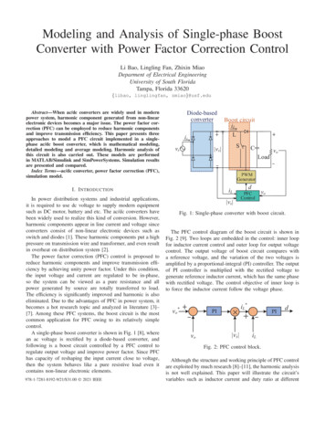
International Journal of Engineering Research & Technology (IJERT)ISSN: 2278-0181Vol. 3 Issue 7, July - 2014Two Stage Interleaved Boost Converter Designand Simulation in CCM and DCMAjit T NPG Student (MTech, Power Electronics)Department of Electrical and Electronics EngineeringReva Institute of Technology and ManagementBangalore, IndiaAbstract— The concept of interleaving, or more generally thatof increasing the effective pulse frequency of any periodic powersource by synchronizing several smaller sources and operatingthem with relative phase shifts, has several advantages. We havea source and a load and the converter in between can have manystages in parallel. Among these the Interleaved Boost Converterhas many applications. Here the concept of interleaving and thedesign and simulation of the Interleaved Boost Converter inboth the CCM and DCM modes are discussed.diodes and inductors connected to a common filter capacitorand load. [4][5]II. WORKING AND ANALYSIS OF INTERLEAVEDBOOST CONVERTERI. INTRODUCTIONIJERTKeywords—Interleaving, Boost Converter, CCM, DCM.In the field of power electronics, application ofinterleaving technique can be traced back to very early days,especially in high power applications. In high powerapplications, the voltage and current stress can easily gobeyond the range that one power device can handle. Multiplepower devices connected in parallel and/or series could beone solution. However, voltage sharing and/or current sharingare still the concerns. Instead of paralleling power devices,paralleling power converters is another solution which couldbe more beneficial. Furthermore, with the power converterparalleling architecture, interleaving technique comesnaturally. Benefits like harmonic cancellation, betterefficiency, better thermal performance, and high powerdensity can be obtained. In earlier days, for high powerapplications, in order to meet certain system requirement,interleaving multi-channel converter could be a superiorsolution especially considering the available power deviceswith limited performance at that time. Interleaving techniquewas also investigated in the early days for the satellite or fuelcell applications [2][3], and was introduced asunconventional SMPS power stage architecture[1].Interleaving technique can effectively reduce the filtercapacitor size and weight.Boost power supplies are popular for creating higher dcvoltages from low-voltage inputs. As the power demandsfrom these supplies increase, however, a single power stagemay be insufficient. Interleaving is also called „multiphasing‟and is useful for reducing the filter components. It isequivalent to a parallel connection of 2 sets of switches,IJERTV3IS070847Fig 1: Single stage and Interleaved Boost convertersThe diagram above shows a Single stage Boost Converterand Interleaved Boost Converter. We can see clearly that inthe Interleaved topology, between the input and output stages,there are 2 stages of the power converter in parallel, therebyhaving 2 inductors, 2 switches and 2 diodes. [6]In the single-phase design, applying a gate voltage toMOSFET Q1 pulls the drain potential to ground, applying theinput voltage across inductor L1 and causing current to rampup. During the ramp time, output capacitor C1 must alonesupply the load current. When Q1 turns off, the voltage acrossL1 reverses polarity to maintain current flow. This scenarioforces the switch node more positive than the input voltageand forward-biases diode D1, charging output capacitor C1and supplying the output current. For each of the twoswitching states, the inductor‟s volt-microsecond productmust balance. That is, d/fS*VIN (1-d)/fS*(VOUT-VIN), yieldingwww.ijert.org847
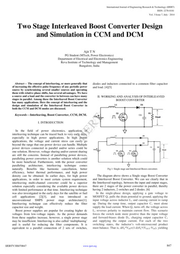
International Journal of Engineering Research & Technology (IJERT)ISSN: 2278-0181Vol. 3 Issue 7, July - 2014the relation VOUT VIN/(1-d), where d is the duty ratio, fS isthe switching frequency, VIN is the input voltage, and VOUT isthe output voltage. This expression is valid in CCM(continuous conduction mode), in which the inductor currentremains positive at all times. Each phase of the interleavedboost converter works in the same way that this single-phaseboost converter does. The two power stages operate 180degree out of phase, cancelling the ripple current in the inputand the output capacitors. The interleaved-boost approachuses forced current-sharing between the power stages toequalize the power that the stages deliver. Without thisfeature, one power stage could deliver substantially morepower than the other, which would defeat the ripplecancellation.The design is done for the ideal condition. Voltage dropacross the diodes and switches is not considered. ESR(Equivalent series resistance) of Capacitor is not considered.Calculation of the parameters:A. Duty cycle (D)Formula for the voltage conversion ratio is as below.VO / Vd 1 / (1-D)D (Vo – Vd) / Vo(1)Dmax (400 – 90 ) / 400 0.775Dmin (400 – 264) / 400 0.34B. Current Ripple ( IL)Load current Io Output power / Output voltageIo 1300 / 400 3.25 ARMS 4.6APeak Io 40 % of load current (4.6A) 1.84 ARelation between input and output currents is as below.IIN Io / (1-D)(2) 2IL Io / (1-D) IL (0.5) Io / (1-D)(3) IL (0.5)3.25/(1- 0.775) 7.22 ARMS 10.21APeakFig 2: Currents of the 2 stages and the effective input currentIJERTFigure above shows that the two power stages areoperating 180 degree out of phase provide a two-to-onereduction in peak-to-peak ripple current. The individualinterleaved power stages operate at the same frequency as thesingle-phase design, 100 kHz, but the effective input- andoutput-ripple frequency is 200 kHz. The interleaved-designcalculation used a frequency of 100 kHz and twice the ripplecurrent of the single-phase design, yielding half theinductance. Since the same input current of the single stage isdividing into two in the interleaved design, the inductorspecifications like current rating, LI2 are greatly reduced [6].The losses are also reduced considerably as the conductionlosses are less compared to the single stage design.(Therefore IIN 2IL 20.42APeak) IL 20 % of IL (10.21A) IL 2.036AC. Inductor valueFor CCM, Output current (IO) should be greater thanthe boundary current (IOB)IO IOBVo / R Ts Vo D (1-D)2 / 2LL min RTs D (1-D)2 / 2(4)Load resistor R Vo / Io 400 / 3.25 123.08 ΩTs (Time period) 1 / fs 1 / 100 KHz 10 µsVd 90 VRMS 127.28VpeakVo 400 VRMS 565.68 VpeakIII. DESIGN OF THE INTERLEAVED BOOSTCONVERTER IN CCM MODEThe minimum value of inductance for CCM is givenby the below formula:The design of the Interleaved Boost Converter inContinuous Conduction mode (CCM) is similar to the designof the single stage normal boost converter with slightdifferences.Lmin RTs D(1-D)2 / 2Lmin (123.08) (10*10-6)(0.775) (1- 0.775)2 / 2Lmin 24.14 µHIf the inductance value is 24.14uH, it will result inboundary condition.The design parameters are as below : Input Voltage (Vd ) range – 90 – 264 VRMS Output Voltage (VO ) - 400 V Output Power – 1.3 KW Switching frequency (of each MOSFET switch) –L VdDTs / IL(5)L (127.28 )(0.775)(10*10-6) / 2.036L 484.5µHAs we can see, this is much greater than theboundary value resulting in CCM100 KHz Voltage ripple – 200mV Current ripple – 40 % of load current [7]IJERTV3IS070847D. Capacitance valueC Io D (Ts/2) / VC (3.25) (0.775) (10*10-6/2) / 0.2C 63 µFwww.ijert.org(6)848
International Journal of Engineering Research & Technology (IJERT)ISSN: 2278-0181Vol. 3 Issue 7, July - 2014The major differences that we see in the design whencompared to the single stage normal boost converter is in thecalculation of the current ripple where the optimal value ischosen to be 40 % of the load current [7]. Hence the inductorcurrent ripple should be chosen as half which is 20% of eachinductor current. Another difference is that while calculatingthe capacitance value we consider Ts/2 as the switchingfrequency doubles and hence time period is halved.is a natural cancellation of the ripple in the interleavedtopology.IV. SIMULATION IN CCMFig 5 : The input current in CCMIJERTFig 3: Simulation circuit of Interleaved Boost Converter in CCMThe inductances L1 and L2 have the same value of484.5µH. Capacitance is 63µF. Duty cycle is 0.775. Thevalues are the ones which have been calculated in the previoussection.Fig 6 : The waveforms of load current and load voltage in CCMAs we can see the waveforms of the load current and loadvoltage are the same which indicates that the power factor ofthe circuit is very near unity or unity. The circuit can be usedwhere Power factor correction is needed.V. DESIGN OF THE INTERLEAVED BOOSTCONVERTER IN DCM MODEFig 4: The inductor currents of the 2 inductors IL1 and IL2 in CCMIt can be seen in Fig 4 above that the inductor currents areoperating at 180 deg out of phase that is while one is charging,the other is discharging. Both the inductor currents IL1 and IL2are not reaching zero which means that the converter is inCCM. The average value of each of the inductor currents is11A. The inductor current ripple is 2A.Fig 5 shows the input current. When compared with theinductor currents, it can be seen that, for the same duty cycle,the switching frequency is doubled and the ripple is reduced.The ripple of the input current is 1.4 A which proves that thereIJERTV3IS070847The design of the Interleaved Boost Converter in theDiscontinuous conduction mode (DCM) is considerablydifferent when compared to the CCM mode. Here also thereare slight modifications to the design as compared to thesingle stage boost converter.The design parameters are the same as in the CCM mode.However when the calculation of the parameters isconcerned, the same order as the CCM mode cannot befollowed.Calculation of the parameters:A. Load current, load resistor, time period and peak values.These calculations are the same as in CCM mode.www.ijert.org849
International Journal of Engineering Research & Technology (IJERT)ISSN: 2278-0181Vol. 3 Issue 7, July - 2014B. Inductor valueWhile calculating the inductance value in the CCM mode,we also calculated the minimum value of inductance Lmin.Now if the value is equal to Lmin, then we will have theboundary condition, where the inductor current just toucheszero and then the next cycle begins immediately. We got Lminas 24.14 µH. So it follows that if the inductor value is lessthan 24.14 µH, then the converter will work in DCM.So let the value of L be 15 µH (which is 24.14 µH)Fig 7 shows the inductor currents of the 2 inductors andthe input current in the Discontinuous Conduction Mode. The2 inductor currents remain at zero for some time during thetime period and hence the DCM mode is confirmed. Both theconverter stages operate at 180 deg phase difference. Theeffective input current does not reach zero as there is noinstance where both the inductor currents are zero at the sametime. The input current ripple is reduced as compared to theinductor currents. This also proves the natural ripple reductionproperty of the interleaving topology.C. Duty CycleIn DCM the formula for the duty cycle is given byD (IO2L(Vo – Vd) / (TsVd2))(7)D (4.6*2*15*10-6*(565.68-127.28) / 10*10-6*127.282)D 0.61D. 1(Percentage of time period where the inductordischarges) 1 Vd / (Vo – Vd) * D(8) 1 (127.28 / (565.68 – 127.28) * 0.61) 1 0.117F. Output capacitor valueC Io D (Ts/2) / VC (4.6)*(0.61) (10*10-6/2) / 0.2C 70.15 µFVI. SIMULATION IN DCM(9)Fig 7: The inductor currents of the 2 inductors IL1 and IL2 and the inputcurrent in DCMIJERTE. Ripple Inductor current ( IL) IL VdDTs / L IL 127.28*0.61*10*10-6 / (15*10-6) IL 51.76A(10)The circuit in DCM is shown by Fig 6.Fig 8: The waveforms of load current and load voltage in DCMAs we can see the waveforms of the load current and loadvoltage are the same which indicates that the power factor ofthe circuit is very near unity or unity. The circuit can be usedwhere Power factor correction is needed.Fig 6: Simulation circuit of Interleaved Boost Converter in DCMThe circuit is the same as that of CCM. The inductancesL1 and L2 have the same value of 15µH. Capacitance is70.15µF. Duty cycle is 0.61. The values are the ones whichhave been calculated in the previous section.IJERTV3IS070847The major differences that we see in the design whencompared with the normal single stage boost converter are thesame as that of CCM mode but when DCM design iscompared to the CCM mode, the way we choose the inductorvalue is different, the formula for the duty cycle is different,and 1 needs to be calculated. Also duty cycle depends on theload in DCM but not so in CCM.www.ijert.org850
International Journal of Engineering Research & Technology (IJERT)ISSN: 2278-0181Vol. 3 Issue 7, July - 2014VII. APPLICATIONSThe Interleaved Boost Converter is used widely incomputer and telecom applications where SMPS (SwitchedMode Power Supplies) are needed. Other applications are inphotovoltaic fuel cells, hybrid electric vehicles and satellites.DCM mode is used when the energy required by the loadis very low i.e. in low power applications.These can be used in power electronic equipments whichrequire power factor correction (PFC).Yungtaek Jang and Milan Jovanovic whose work inspired meto work on the design on interleaved converters.REFERENCES[1][2][3]VIII. CONCLUSIONThe interleaved boost converter in both the continuousconduction mode (CCM) and in the discontinuous conductionmode (DCM) has been successfully designed and simulated toverify the design. The two-phase approach uses significantlyless inductance than does the single-phase approach, and eachinductor carries half the current. There is a natural reduction inthe ripple of the input and output currents.[4][5][6]ACKNOWLEDGMENT[7][8]IJERTI would like to thank the authors of the reference paperInterleaved Boost Converter with Intrinsic voltage doublercharacteristic for Universal Line PFC front end– IEEE 2007,G. Yungtaek Jang and Milan Jovanovic, “Interleaved boost converterwith intrinsic voltage doubler characteristic” in IEEE transactions onPower Electronics, Vol 22, no. 4, July 2007, pp1394 – 1401Gyu-Yeong Choe, Jong-Soo Kim, Hyun-Soo Kang and Byoung-KukLee,“ An optimal design methodology of an interleaved boost converterfor fuel cell applications,” in Journal of Electrical Engineering &Technology Vol. 5, No. 2, pp. 319 328, 2010.Ahmad Saudi Samosir, Taufiq, Abd Jaafar Shafie, Abdul Halim MohdYatim, “Simulation and implementation ofiInterleaved boost DC-DCconverter for fuel cell application,” International Journal of PowerElectronics and Drive System (IJPEDS) Vol.1, No.2, December 2011,pp. 168 174Daniel Hart, Power Electronics, Tata McGraw Hill Edition 2011, NewYork.N. Mohan, T. M Undeland and W.P Robbins , Power Electronics:Converters, Applications and Design, 3rd Edition., Wiley, New York,2003John Betten, Robert Kollman, “Interleaving DC-DC converters boostefficiency and voltage”, Application report, Texas Instruments.Ronald Crews, “AN-1820 LM5032 Interleaved Boost Converter”,Application report, Texas Instruments, May 847www.ijert.org851
BOOST. CONVERTER. IN. CCM. MODE. The design of the Interleaved Boost Converter in Continuous Conduction mode (CCM) is similar to the design of the single stage normal boost converter with slight differences. The design parameters are as below : Input Voltage (Vd ) range - 90 - 264 V RMS Output Voltage (V O) - 400 V