Transcription
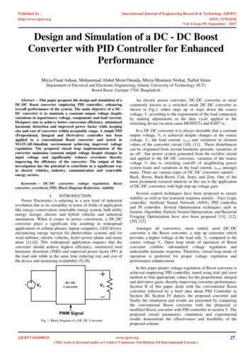
Published by :http://www.ijert.orgInternational Journal of Engineering Research & Technology (IJERT)ISSN: 2278-0181Vol. 6 Issue 09, September - 2017Design and Simulation of a DC - DC BoostConverter with PID Controller for EnhancedPerformanceMirza Fuad Adnan, Mohammad Abdul Moin Oninda, Mirza Muntasir Nishat, Nafiul IslamDepartment of Electrical and Electronic Engineering, Islamic University of Technology (IUT)Board Bazar, Gazipur-1704, BangladeshAbstract— This paper proposes the design and simulation of aDC-DC Boost converter employing PID controller, enhancingoverall performance of the system. The main objective of a DCDC converter is to maintain a constant output voltage despitevariations in input/source voltage, components and load current.Designers aim to achieve better conversion efficiency, minimizedharmonic distortion and improved power factor while keepingsize and cost of converter within acceptable range. A simple PID(Proportional, Integral and Derivative) controller has beenapplied to a conventional Boost converter and tested inMATLAB-Simulink environment achieving improved voltageregulation. The proposed closed loop implementation of theconverter maintains constant output voltage despite changes ininput voltage and significantly reduces overshoot therebyimproving the efficiency of the converter. The output of thisinvestigation has the potential to contribute in a significant wayin electric vehicles, industry, communication and renewableenergy sectors.Keywords— DC-DC converter; voltage regulation; Boostconverter; overshoot; PID; Block Diagram Reduction; stabilityI.INTRODUCTIONPower Electronics is ushering in a new kind of industrialrevolution due to its versatility in terms of fields of applicationlike energy conservation, renewable energy system, bulk utilityenergy storage, electric and hybrid vehicles and industrialautomation. When it comes to power conversion, a DC-DCconverter plays a significant role resulting in widespreadapplications in cellular phones, laptop computers, LED drivers,maximizing energy harvest for photovoltaic systems and forwind turbines, electric vehicles, hydro power plants and manymore [1]-[4]. This widespread application requires that theconverter should achieve highest efficiency, minimized totalharmonic distortion (THD) and improved power factor (PF) atthe load side while at the same time reducing size and cost ofthe device and increasing availability [5]-[8].Fig. 1. Block Diagram of a DC-DC ConverterIJERTV6IS090029An electric power converter, DC-DC converter or morecommonly known as a switched mode DC-DC converter asshown in Fig.1, either steps up or steps down the sourcevoltage, Vs according to the requirement of the load connected,by making adjustments in the duty cycle applied to theswitching device (in most cases MOSFETs and IGBT’s).In a DC-DC converter it is always desirable that a constantoutput voltage, Vo is achieved despite changes in the sourcevoltage, Vs, the load current, iLoad and variations in elementvalues of the converter circuit [10], [11]. These disturbancescan be originated from second harmonic periodic variations ofan off - line power system generated from the rectifier circuitand applied to the DC-DC converter, variation of the sourcevoltage Vs due to switching (on/off) of neighboring powersystem loads and variations in the load current, iLoad amongstmany. There are various types of DC-DC converters namely –Buck, Boost, Buck-Boost, Cuk, Sepic and Zeta. One of themost prominent research interests in this era is the applicationof DC-DC converters with high step-up voltage gain.Several control techniques have been proposed to ensurestability as well as fast transient response namely - Fuzz Logiccontroller, Artificial Neural Network (ANN), PID controllerand PI controller. Several Optimization techniques such asGenetic Algorithm, Particle Swarm Optimization, and BacterialForaging Optimization have also been proposed [11], [12],[20], [21].Amongst all converters, most widely used DC-DCconverter is the Boost converter, a step up converter whichprovides a higher voltage at the load side, Vo compared to thesource voltage Vs. Open loop mode of operation of Boostconverter exhibits substandard voltage regulation andundesirable dynamic response. Therefore, closed loop mode ofoperation is preferred for proper voltage regulation andperformance enhancement.In this paper proper voltage regulation of Boost converter isachieved employing PID controller, tuned using trial and errormethod to find appropriate values for the proportional, integraland derivative gains, thereby improving converter performance.Section II of this paper deals with the conventional Boostconverter followed by a brief idea about PID Controller inSection III, Section IV depicts the proposed converter andfinally the simulation and results are presented by comparingthe conventional Boost converter with the proposed ormodified Boost converter with PID controller in section V. Theproposed circuit parameters, simulation and experimentalresults demonstrate the effectiveness and feasibility of theproposed scheme.www.ijert.org(This work is licensed under a Creative Commons Attribution 4.0 International License.)27
Published by :http://www.ijert.orgInternational Journal of Engineering Research & Technology (IJERT)ISSN: 2278-0181Vol. 6 Issue 09, September - 2017II. CONVENTIONAL BOOST CONVERTERA conventional DC-DC Boost converter is composed of aboost inductor, two semiconductors (a diode and a transistor)and an output capacitor in parallel with the load as shown inFig. 2.Transistor switching period is given byMode 1Ton DTpMode 2Toff 1 D Tp(1)Voltage across the inductor,LMode 1di VidtdiL (Vi Vo )dtMode 2(2)Putting equation (1) in equation (2)LMode 1LMode 2Fig. 2. Conventional Boost ConverterBoost converter also known as an up converter provides anoutput voltage that is greater than the input voltage. Input for aboost converter can be a simple DC source such as a battery,solar panel or can be obtained directly from an AC sourcethrough a rectifier. The inductors tendency to resist currentvariations due to changes in the magnetic field is the keyprinciple that drives the Boost converter. Boost converter issaid to operate in two modes. The switching is achieved usingeither a MOSFET or an IGBT. In low voltage applicationsMOSFET is preferred over IGBT due to its highercomputational speed compared to IGBT. Modes of operation ofBoost converter is as follows: Mode 1 begins at t 0s when the transistor is switchedon causing the rising input current to flow through theinductor L, storing energy in its magnetic field. Duringthis mode of operation as shown in Fig. 3(a) the loadside is completely isolated from the source side.Mode 2 begins at t t1 when the transistor is switchedoff. Inductor, L produces a back emf having oppositepolarity of the Mode 1 due to rapid drop in current. Thevoltage across the inductor and the source minus thesmall forward voltage drop across the diode, D chargesthe capacitor, C and also supplies the load. Theconduction path is shown in Fig. 3(b).Ripple current i ViDTp i Vo Vi(1 D)Tp i , is given by ion Mode 1 ioff Mode 2Vi DTpL(1 D)(Vo Vi )Tp(3)(4)LEquating the ripple current equation (3) and (4) of Mode 1 and Mode 2 ion ioffVi D Vo Vi DVo DViVi Vo DVoVi Vo (1 D)Vo1 Vi 1 D(5)Where,ViVotonInput Voltage, VtoffMOSFET off, secTpSwitching Period, secD iDuty CycleRipple currentOutput Voltage, VMOSFET on, secIII.PID CONTROLLEROne of the simplest and most widely used controller fordecades is the PID controller. PID stands for proportional (P),integral (I) and derivative (D) controller. Fig. 4 shows the blockdiagram of a typical PID controller.Fig. 4. Typical PID control StructureFig. 3. Mode of operation of Boost ConverterIJERTV6IS090029www.ijert.org(This work is licensed under a Creative Commons Attribution 4.0 International License.)28
Published by :http://www.ijert.orgInternational Journal of Engineering Research & Technology (IJERT)ISSN: 2278-0181Vol. 6 Issue 09, September - 2017The system under study is the plant to which necessaryexcitation is provided thereby achieving overall closed loopcontrol effectively. A PID can be expressed as –KD s2 KP s KIsKIC s KP KDssoperating machines in industries and researchers aim fordesigning a converter with good voltage regulation andovershoot reduction.C s (6)Where,KPProportional gainKIKDIntegral gain(a)Derivative GainThe signal e(t) as shown in Fig. 4 represents the trackingerror obtained from the difference between the reference signalwhich serves as the input R(t) and the actual output signalVo(t). The tracking error is fed on to the PID controller whichcomputes the derivative and integral of the signal provided.The output of the PID controller u(t) to be applied to the plantis equal to the proportional gain (KP) times the magnitude ofthe error signal plus the integral gain (KI) times the integral ofthe error signal plus the derivative gain (KD) times thederivative of the error signal.(b)Time domain representation of the signal u(t) fed to theplant is given by –u (t ) K P e t K I e(t )dt K Dde(t )dt(7)The plant on receiving the signal u(t) will generate amodified output Vo(t) which will be again compared to thereference signal until the desired level is reached therebyforming a close loop system. Effect of proportional, integraland derivative control on close loop system is summarized inthe Table I. provided below.TABLE I.EFFECT OF PID ON CLOSE LOOP SYSTEMSteadySettlingState ErrorRise Change(d)Fig. 5. Block diagram reduction of proposed PID controllerThe controllers can be implemented individually as well asin combination, with the converters to obtain the desired result.IV. PROPOSED CONVERTERThe proposed converter as shown in Fig. 6 is similar to theconventional Boost converter as shown in Fig. 2 but differsonly in the incorporation of a PID controller which isextensively used in many practical applications for betterperformance. The proposed PID controller has been obtainedby block diagram reduction method in four stages as shown inFig. 5. The first figure, Fig. 5(a) depicts a conventional PIDcontroller block diagram when in successive stages as shown inFig. 5(b), Fig. 5(c) and Fig. 5(d), by block diagram reductiontechnique the proposed control scheme for the Boost converterwas obtained as shown in Fig. 5(d) which is feasible forproposed converter. Initial overshoot is a prime concern forIJERTV6IS090029Fig. 6. Proposed Boost converter with PID controller for voltage regulation andovershoot reductionwww.ijert.org(This work is licensed under a Creative Commons Attribution 4.0 International License.)29
Published by :http://www.ijert.orgInternational Journal of Engineering Research & Technology (IJERT)ISSN: 2278-0181Vol. 6 Issue 09, September - 2017Incorporating a PID controller with the converter improvesthe dynamic response and reduces the steady-state error. Thederivative controller (KD) ameliorates the transient responseand the integral controller (KI) will reduce the steady state errorof the system. Our proposed system maintains an output of200V when the input is in the range of 90V-110V which makesit quite feasible to apply in different industrial purposes.V. RESULT AND SIMULATIONSimulation was done in MATLAB-Simulink environment.The parameters used for this simulation are given Table II. asshown below –TABLE II.SIMULATION PARAMETERSParameterValueInput Voltage90V-110VOutput Voltage200VRated Power800WDuty cycle0.5Boost Inductor400µHFilter Capacitor100µResistive Load50ΩKP0.0033KI6.43KD0.0027(b)Conventional Boost converter as shown in Fig. 7, wassimulated at 50% duty cycle and the output wave shapesobserved for variations of input voltage from 90V – 110V withincrement of 10V. It can be observed that the output voltagefluctuates with variation of input voltage by a large amount.Moreover the converter exhibits significant increase inovershoot as the input voltage varies as shown in Fig. 8.(c)Fig. 8. Output voltage plot of conventional Boost converter operating at 50%duty cycle for input voltages (a) 90V, (b) 100V and (c) 110VFig. 7. MATLAB-Simulink model of conventional Boost converterFor proper voltage regulation and overshoot reduction theproposed Boost converter as shown in Fig. 9, was simulated forinput voltage 90V – 110 V with increments of 10V and outputwave shapes observed as shown in Fig. 10. It can be observedthat the output voltage remains constant at the desired voltageof 200V and does not vary with variation of input voltage.Moreover, a significant reduction is overshoot has also beenobserved.Fig. 9. MATLAB-Simulink model of proposed Boost converter with PIDcontroller(a)IJERTV6IS090029www.ijert.org(This work is licensed under a Creative Commons Attribution 4.0 International License.)30
Published by :http://www.ijert.orgInternational Journal of Engineering Research & Technology (IJERT)ISSN: 2278-0181Vol. 6 Issue 09, September - 2017Simulation data obtained as shown in Table III was plottedin MATLAB and comparison was done between conventionaland proposed Boost converter in terms of output voltage asshown in Fig. 11 and percentage overshoot as shown in Fig. 12.TABLE III.InputVoltage, Vi(V)90100110COMPARISON BETWEEN CONVENTIONAL ANDPROPOSED BOOST CONVERTERConventionalOutputPercentageVoltage, posedOutputPercentageVoltage, . 11. Output voltage comparison between conventional and proposed Boostconverter(b)Fig. 12. Percentage overshoot comparison between conventional andproposed Boost converterExperimental results show that the proposed PID controllerwhen used with Boost converter provides better output voltageregulation and overshoot reduction, thereby improving theperformance of the system.VI. CONCLUSIONThe proposed Boost converters with PID controllerprovides better voltage regulation, overshoot reduction andimproves the converter performance compared to theconventional Boost converter. This paper successfully providesa method to satisfy the objective of DC-DC converter tomaintain a constant output voltage at the load side. Theproposed circuit is simple, easy to understand and can beimplemented with no additional components thereby keepingsize and cost of manufacturing the converter withinconsiderable range.(c)Fig. 10. Output voltage plot of proposed Boost converter with PID controlleroperating at 50% duty cycle for input voltages (a) 90V, (b) 100V and (c) 110VIJERTV6IS090029www.ijert.org(This work is licensed under a Creative Commons Attribution 4.0 International License.)31
Published by :http://www.ijert.orgInternational Journal of Engineering Research & Technology (IJERT)ISSN: 2278-0181Vol. 6 Issue 09, September - 2017REFERENCES[1]Kumar, J. Sai, and Tikeshwar Gajpal. "A Multi Input DC-DC Converterfor Renewable Energy Applications." (2016).[2] Ortiz, G., J. Biela, D. Bortis, and J. W. Kolar. "1 Megawatt, 20 kHz,isolated, bidirectional 12kV to 1.2 kV DC-DC converter for renewableenergy applications." In Power Electronics Conference (IPEC), 2010International, pp. 3212-3219. IEEE, 2010.[3] Li, Wuhua, Xiaodong Lv, Yan Deng, Jun Liu, and Xiangning He. "Areview of non-isolated high step-up DC/DC converters in renewableenergy applications." In Applied Power Electronics Conference andExposition, 2009. APEC 2009. Twenty-Fourth Annual IEEE, pp. 364369. IEEE, 2009.[4] Koutroulis, Eftichios, and Kostas Kalaitzakis. "Design of a maximumpower tracking system for wind-energy-conversion applications." IEEEtransactions on industrial electronics 53, no. 2 (2006): 486-494.[5] Ferdous, S. M., Mohammad Abdul Moin Oninda, Golam Sarowar, KaziKhairul Islam, and Md Ashraful Hoque. "Non-isolated single stage PFCbased LED driver with THD minimization using Cúk converter."In Electrical and Computer Engineering (ICECE), 2016 9th InternationalConference on, pp. 471-474. IEEE, 2016.[6] Yang, Bo, Fred C. Lee, A. J. Zhang, and Guisong Huang. "LLC resonantconverter for front end DC/DC conversion." In Applied PowerElectronics Conference and Exposition, 2002. APEC 2002. SeventeenthAnnual IEEE, vol. 2, pp. 1108-1112. IEEE, 2002.[7] Wei, Huai, and Issa Batarseh. "Comparison of basic converter topologiesfor power factor correction." In Southeastcon'98. Proceedings. IEEE, pp.348-353. IEEE, 1998.[8] Daniele, Matteo, Praveen K. Jain, and Geza Joos. "A single-stage powerfactor-corrected AC/DC converter." IEEE Transactions on PowerElectronics 14, no. 6 (1999): 1046-1055.[9] Rathi, Ms Kashmira, and Dr MS Ali. "Design and Simulation of PIDController for Power Electronics Converter Circuits." InternationalJournal Of Innovative And Emerging Research In Engineering 3, no. 2(2016): 26-31.[10] Dave, Mitulkumar R., and K. C. Dave. "Analysis of boost converterusing pi control algorithms." International Journal of Engineering Trendsand Technology 3.2 (2012): 71-73.IJERTV6IS090029[11] Raviraj, V. S. C., and Paresh C. Sen. "Comparative study ofproportional-integral, sliding mode, and fuzzy logic controllers forpower converters." IEEE Transactions on Industry Applications 33, no. 2(1997): 518-524.[12] Meena, Rajendra. "Simulation study of boost converter with variouscontrol techniques." International Journal of Science and Research(IJSR) 3, no. 9 (2014): 74-79.[13] W. Lu, S. Lang, L. Zhou, H. H. C. Iu and T. Fernando, "Improvement ofStability and Power Factor in PCM Controlled Boost PFC ConverterWith Hybrid Dynamic Compensation," in IEEE Transactions on Circuitsand Systems I: Regular Papers, vol. 62, no. 1, pp. 320-328, Jan. 2015.[14] Z. Guo, X. Ren, Y. Wu, Z. Zhang and Q. Chen, "A novel simplifiedvariable on-time method for CRM boost PFC converter," 2017 IEEEApplied Power Electronics Conference and Exposition (APEC), Tampa,FL, USA, 2017, pp. 1778-1784.[15] T. Meng; H. Ben; Y. Song, "Investigation and Implementation of aStarting and Voltage Spike Suppression Scheme for Three-PhaseIsolated Full-Bridge Boost PFC Converter," in IEEE Transactions onPower Electronics , vol.PP, no.99, pp.1-1.[16] I. H. Kim and Y. I. Son, "Regulation of a DC/DC Boost ConverterUnder Parametric Uncertainty and Input Voltage Variation Using NestedReduced-Order PI Observers," in IEEE Transactions on IndustrialElectronics, vol. 64, no. 1, pp. 552-562, Jan. 2017.[17] J. Ma, M. Zhu, J. Zhang and X. Cai, "Improved asynchronous voltageregulation strategy of non-inverting Buck-Boost converter for renewableenergy integration," 2015 IEEE 2nd International Future EnergyElectronics Conference (IFEEC), Taipei, 2015, pp. 1-5.[18] A. Singh, A. A. Milani and B. Mirafzal, "Voltage regulation in singlestage boost inverter for stand-alone applications," 2014 IEEE AppliedPower Electronics Conference and Exposition - APEC 2014, Fort Worth,TX, 2014, pp. 3011-3016.[19] O. Ibrahim, N. Z. Yahaya and N. Saad, "Comparative studies of PIDcontroller tuning methods on a DC-DC boost converter," 2016 6thInternational Conference on Intelligent and Advanced Systems (ICIAS),Kuala Lumpur, 2016, pp. 1-5.[20] L. Mitra and N. Swain, "Closed loop control of solar powered boostconverter with PID controller," 2014 IEEE International Conference onPower Electronics, Drives and Energy Systems (PEDES), Mumbai,2014, pp. 1-5.[21] P. Verma, N. Patel, N. K. C. Nair and A. Sikander, "Design of PIDcontroller using cuckoo search algorithm for buck-boost converter ofLED driver circuit," 2016 IEEE 2nd Annual Southern Power ElectronicsConference (SPEC), Auckland, 2016, pp. 1-4.www.ijert.org(This work is licensed under a Creative Commons Attribution 4.0 International License.)32
A conventional DC-DC Boost converter is composed of a boost inductor, two semiconductors (a diode and a transistor) and an output capacitor in parallel with the load as shown in Fig. 2. Fig. 2. Conventional Boost Converter , is given by Boost converter also known as an up converter provides an output voltage that is greater than the input voltage.