Transcription
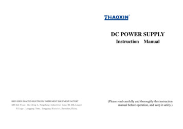
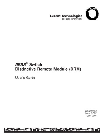
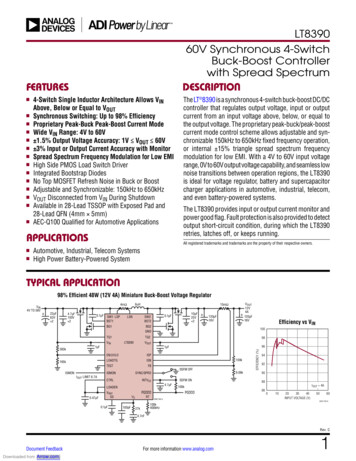
LT839060V Synchronous 4-SwitchBuck-Boost Controllerwith Spread SpectrumDESCRIPTIONFEATURESnnnnnnnnnnnnnn4-Switch Single Inductor Architecture Allows VINAbove, Below or Equal to VOUTSynchronous Switching: Up to 98% EfficiencyProprietary Peak-Buck Peak-Boost Current ModeWide VIN Range: 4V to 60V 1.5% Output Voltage Accuracy: 1V VOUT 60V 3% Input or Output Current Accuracy with MonitorSpread Spectrum Frequency Modulation for Low EMIHigh Side PMOS Load Switch DriverIntegrated Bootstrap DiodesNo Top MOSFET Refresh Noise in Buck or BoostAdjustable and Synchronizable: 150kHz to 650kHzVOUT Disconnected from VIN During ShutdownAvailable in 28-Lead TSSOP with Exposed Pad and28-Lead QFN (4mm 5mm)AEC-Q100 Qualified for Automotive ApplicationsAPPLICATIONSnnThe LT 8390 is a synchronous 4-switch buck-boost DC/DCcontroller that regulates output voltage, input or outputcurrent from an input voltage above, below, or equal tothe output voltage. The proprietary peak-buck/peak-boostcurrent mode control scheme allows adjustable and synchronizable 150kHz to 650kHz fixed frequency operation,or internal 15% triangle spread spectrum frequencymodulation for low EMI. With a 4V to 60V input voltagerange, 0V to 60V output voltage capability, and seamless lownoise transitions between operation regions, the LT8390is ideal for voltage regulator, battery and supercapacitorcharger applications in automotive, industrial, telecom,and even battery-powered systems.The LT8390 provides input or output current monitor andpower good flag. Fault protection is also provided to detectoutput short-circuit condition, during which the LT8390retries, latches off, or keeps running.All registered trademarks and trademarks are the property of their respective owners.Automotive, Industrial, Telecom SystemsHigh Power Battery-Powered SystemTYPICAL APPLICATION98% Efficient 48W (12V 4A) Miniature Buck-Boost Voltage RegulatorVIN4V TO 56V6uH4mΩ22µF63V 24.7µF100V 20.1µFSW1 LSPBST1LSNVOUT12V4A120µF16V15mΩBG110µF25V 20.1µFSW2BST2120µF16VEfficiency vs PLOADTGISNTESTIOUT LIMIT 6.7A98VOUT100kFBISMONSSFM OFFSYNC/SPRDCTRLINTVCCSSFM µF100kPGOOD8390 TA01a9.09kEFFICIENCY (%)TG19492908886IOUT 4A010203040INPUT VOLTAGE (V)50608390 TA01b100k400kHz27k4.7nFRev. CDocument FeedbackDownloaded from Arrow.com.For more information www.analog.com1
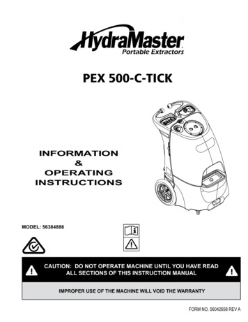
LT8390ABSOLUTE MAXIMUM RATINGS(Note 1)VIN, EN/UVLO, VOUT, ISP, ISN.60V FB, LOADEN, SYNC/SPRD, CTRL, PGOOD.6V(ISP-ISN).–1V to 1V Operating Junction Temperature Range (Notes 2, 3)BST1, BST2.66VLT8390E. –40 C to 125 CLT8390I. –40 C to 125 CSW1, SW2, LSP, LSN. –6V to 60VLT8390J, LT8390H. –40 C to 150 CINTVCC, (BST1-SW1), (BST2-SW2).6V(BST1-LSP), (BST1-LSN).6V Storage Temperature Range. –65 C to 150 CPIN CONFIGURATIONTOP VIEWTOP VIEW26 SW2TG1425 TG2TG1 122 TG2LSP524 VOUTLSP 221 VOUT23 LOADTGLSN 320 LOADTG8EN/UVLO21 RTINTVCC 5920 VCEN/UVLO 6TEST 1019 FBLOADEN 1118 SS17 PGOODCTRL 1316 ISMONISP 1418 RT17 VCTEST 716 FBLOADEN 815 SS9 10 11 12 13 14VREFVREF 1219 SYNC/SPRD29GND15 ISNFE PACKAGE28-LEAD PLASTIC TSSOPθJA 30 C/W, θJC 5 C/WEXPOSED PAD (PIN 29) IS GND, MUST BE SOLDERED TO PCBPGOODINTVCC22 SYNC/SPRDISMON7VIN 4ISNVIN29GNDISP628 27 26 25 24 23CTRLLSNSW227 BST23BST22SW1BG2BST1BG128 BG2BST11SW1BG1UFD PACKAGE28-LEAD (4mm 5mm) PLASTIC QFNθJA 43 C/W, θJC 3.4 C/WEXPOSED PAD (PIN 29) IS GND, MUST BE SOLDERED TO PCBORDER INFORMATIONLEAD FREE FINISHTAPE AND REELPART MARKING*PACKAGE DESCRIPTIONTEMPERATURE RANGELT8390EFE#PBFLT8390EFE#TRPBFLT8390FE28-Lead Plastic TSSOP–40 C to 125 CLT8390IFE#PBFLT8390IFE#TRPBFLT8390FE28-Lead Plastic TSSOP–40 C to 125 CLT8390JFE#PBFLT8390JFE#TRPBFLT8390FE28-Lead Plastic TSSOP–40 C to 150 CLT8390HFE#PBFLT8390HFE#TRPBFLT8390FE28-Lead Plastic TSSOP–40 C to 150 CLT8390EUFD#PBFLT8390EUFD#TRPBF839028-Lead (4mm 5mm) Plastic QFN–40 C to 125 CLT8390IUFD#PBFLT8390IUFD#TRPBF839028-Lead (4mm 5mm) Plastic QFN–40 C to 125 CLT8390JUFD#PBFLT8390JUFD#TRPBF839028-Lead (4mm 5mm) Plastic QFN–40 C to 150 CLT8390HUFD#PBFLT8390HUFD#TRPBF839028-Lead (4mm 5mm) Plastic QFN–40 C to 150 C2Downloaded from Arrow.com.Rev. CFor more information www.analog.com
LT8390ORDER INFORMATIONLEAD FREE FINISHTAPE AND REELPART MARKING*PACKAGE DESCRIPTIONTEMPERATURE RANGELT8390EFE#WPBFLT8390EFE#WTRPBFLT8390FE28-Lead Plastic TSSOP–40 C to 125 CLT8390IFE#WPBFLT8390IFE#WTRPBFLT8390FE28-Lead Plastic TSSOP–40 C to 125 CLT8390JFE#WPBFLT8390JFE#WTRPBFLT8390FE28-Lead Plastic TSSOP–40 C to 150 CLT8390HFE#WPBFLT8390HFE#WTRPBFLT8390FE28-Lead Plastic TSSOP–40 C to 150 CLT8390EUFD#WPBFLT8390EUFD#WTRPBF839028-Lead (4mm 5mm) Plastic QFN–40 C to 125 CLT8390IUFD#WPBFLT8390IUFD#WTRPBF839028-Lead (4mm 5mm) Plastic QFN–40 C to 125 CLT8390JUFD#WPBFLT8390JUFD#WTRPBF839028-Lead (4mm 5mm) Plastic QFN–40 C to 150 CLT8390HUFD#WPBFLT8390HUFD#WTRPBF839028-Lead (4mm 5mm) Plastic QFN–40 C to 150 CAUTOMOTIVE PRODUCTS**Contact the factory for parts specified with wider operating temperature ranges. *The temperature grade is identified by a label on the shipping container.Tape and reel specifications. Some packages are available in 500 unit reels through designated sales channels with #TRMPBF suffix.**Versions of this part are available with controlled manufacturing to support the quality and reliability requirements of automotive applications. Thesemodels are designated with a #W suffix. Only the automotive grade products shown are available for use in automotive applications. Contact yourlocal Analog Devices account representative for specific product ordering information and to obtain the specific Automotive Reliability reports forthese models.ELECTRICAL CHARACTERISTICSThe l denotes the specifications which apply over the full operatingtemperature range, otherwise specifications are at TA 25 C (Note 2). VIN 12V, VEN/UVLO 1.5V unless otherwise noted.PARAMETERSupplyVIN Operating Voltage RangeVIN Quiescent CurrentVOUT Voltage RangeVOUT Quiescent CurrentLinear RegulatorsINTVCC Regulation VoltageINTVCC Load RegulationINTVCC Line RegulationINTVCC Current LimitINTVCC Dropout Voltage (VIN – INTVCC)INTVCC Undervoltage Lockout ThresholdINTVCC Undervoltage Lockout HysteresisVREF Regulation VoltageVREF Load RegulationVREF Line RegulationVREF Current LimitVREF Undervoltage Lockout ThresholdVREF Undervoltage Lockout HysteresisCONDITIONSMINl4VEN/UVLO 0.3VVEN/UVLO 1.1VNot Switching12702.1lVEN/UVLO 0.3V, VOUT 12VVEN/UVLO 1.1V, VOUT 12VNot Switching, VOUT 12V020IINTVCC 20mAIINTVCC 0mA to 80mAIINTVCC 20mA, VIN 6V to 60VVINTVCC 4.5VIINTVCC 20mA, VIN 4VFallingIVREF 100µAIVREF 0mA to 1mAIVREF 100µA, VIN 4V to 60VVREF AV%%mAmVVVV%%mAVmVRev. CFor more information www.analog.comDownloaded from Arrow.com.3
LT8390ELECTRICAL CHARACTERISTICSThe l denotes the specifications which apply over the full operatingtemperature range, otherwise specifications are at TA 25 C (Note 2). VIN 12V, VEN/UVLO 1.5V unless otherwise noted.PARAMETERControl Inputs/OutputsEN/UVLO Shutdown ThresholdEN/UVLO Enable ThresholdEN/UVLO Enable HysteresisEN/UVLO Hysteresis CurrentCTRL Input Bias CurrentCTRL Latch-Off ThresholdCTRL Latch-Off HysteresisLoad Switch DriverLOADEN ThresholdLOADEN HysteresisMinimum VOUT for LOADTG to be OnLOADTG On Voltage V(VOUT-LOADTG)LOADTG Off Voltage V(VOUT-LOADTG)LOADEN to LOADTG Turn On Propagation DelayLOADEN to LOADTG Turn Off Propagation DelayLOADTG Turn On Fall TimeLOADTG Turn Off Rise TimeError AmplifierFull Scale Current Regulation V(ISP-ISN)1/10th Current Regulation V(ISP-ISN)ISMON Monitor Output VISMONISP/ISN Input Common Mode RangeISP/ISN Low Side to High Side Switchover VoltageISP/ISN High Side to Low Side Switchover VoltageISP Input Bias CurrentISN Input Bias CurrentISP/ISN Current Regulation Amplifier gmFB Regulation VoltageFB Line RegulationFB Load RegulationFB Voltage Regulation Amplifier gmFB Input Bias CurrentVC Output ImpedanceVC Standby Leakage Current4Downloaded from 4VEN/UVLO 0.3VVEN/UVLO 1.1VVEN/UVLO 1.3VVCTRL 0.75V, Current Out of lFallingVLOADEN 5VVOUT 12VVOUT 12VCLOADTG 3.3nF to VOUT, 50% to 50%CLOADTG 3.3nF to VOUT, 50% to 50%CLOADTG 3.3nF to VOUT, 10% to 90%CLOADTG 3.3nF to VOUT, 90% to 10%VCTRL 2V, VISP 12VVCTRL 2V, VISP 0VVCTRL 0.35V, VISP 12VVCTRL 0.35V, VISP 0VV(ISP-ISN) 100mV, VISP 12V/0VV(ISP-ISN) 10mV, VISP 12V/0VV(ISP-ISN) 0mV, VISP 12V/0V4.6–0.1llllllll9797881.200.300.200VISP VISNVISP VISNVLOADEN 5V, VISP VISN 12VVLOADEN 5V, VISP VISN 0VVEN/UVLO 0V, VISP VISN 12V or 0VVLOADEN 5V, VISP VISN 12VVLOADEN 5V, VISP VISN 0VVEN/UVLO 0V, VISP VISN 12V or 0VVC 1.2VVIN 4V to 60Vl0.985FB in Regulation, Current Out of PinVC 1.2V, VLOADEN ev. CFor more information www.analog.com
LT8390ELECTRICAL CHARACTERISTICSThe l denotes the specifications which apply over the full operatingtemperature range, otherwise specifications are at TA 25 C (Note 2). VIN 12V, VEN/UVLO 1.5V unless otherwise noted.PARAMETERCurrent ComparatorMaximum Current Sense Threshold V(LSP-LSN)Reverse Current Sense Threshold V(LSP-LSN)LSP Pin Bias CurrentLSN Pin Bias CurrentFaultFB Overvoltage Threshold (VFB)FB Overvoltage HysteresisFB Short Threshold (VFB)FB Short HysteresisISP/ISN Over Current Threshold V(ISP-ISN)PGOOD Upper Threshold Offset from VFBPGOOD Lower Threshold Offset from VFBPGOOD Pull-Down ResistanceSS Hard Pull-Down ResistanceSS Pull-Up CurrentSS Pull-Down CurrentSS Fault Latch-Off ThresholdSS Fault Reset ThresholdOscillatorRT Pin VoltageSwitching FrequencySYNC FrequencySYNC/SPRD Input Bias CurrentSYNC/SPRD Threshold VoltageHighest Spread Spectrum Above Oscillator FrequencyLowest Spread Spectrum Below Oscillator FrequencyRegion TransitionBuck-Boost to Boost (VIN /VOUT)Boost to Buck-Boost (VIN /VOUT)Buck to Buck-Boost (VIN /VOUT)Buck-Boost to Buck (VIN /VOUT)Peak-Buck to Peak-Boost (VIN /VOUT)Peak-Boost to Peak-Buck (VIN /VOUT)CONDITIONSMINTYPMAXUNITSBuck, VFB 0.8VBoost, VFB 0.8VBuck, VFB 0.8VBoost, VFB 0.8VVLSP VLSN 12VVLSP VLSN ISP 12VRisingFallingllllVEN/UVLO 1.1VVFB 0.4V, VSS 0VVFB 0.1V, VSS 2VRT 100kΩVSYNC/SPRD 0V, RT 226kΩVSYNC/SPRD 0V, RT 100kΩVSYNC/SPRD 0V, RT 59.0kΩVSYNC/SPRD 5VVSYNC/SPRD 5VVSYNC/SPRD zkHzkHzkHzµAV%%Rev. CFor more information www.analog.comDownloaded from Arrow.com.5
LT8390ELECTRICAL CHARACTERISTICSThe l denotes the specifications which apply over the full operatingtemperature range, otherwise specifications are at TA 25 C (Note 2). VIN 12V, VEN/UVLO 1.5V unless otherwise noted.PARAMETERNMOS DriversTG1, TG2 Gate Driver On-ResistanceGate Pull-UpGate Pull-DownBG1, BG2 Gate Driver On-ResistanceGate Pull-UpGate Pull-DownTG1, TG2 Rise TimeTG1, TG2 Fall TimeBG1, BG2 Rise TimeBG1, BG2 Fall TimeTG Off to BG On DelayBG Off to TG On DelayTG1 Minimum Duty Cycle in Buck RegionTG1 Maximum Duty Cycle in Buck RegionTG1 Fixed Duty Cycle in Buck-Boost RegionBG2 Fixed Duty Cycle in Buck-Boost RegionBG2 Minimum Duty Cycle in Boost RegionBG2 Maximum Duty Cycle in Boost RegionCONDITIONSMINV(BST-SW) 5VVINTVCC 5VCL 3.3nF, 10% to 90%CL 3.3nF, 90% to 10%CL 3.3nF, 10% to 90%CL 3.3nF, 90% to 10%CL 3.3nFCL 3.3nFPeak-Buck Current ModePeak-Buck Current ModePeak-Boost Current ModePeak-Buck Current ModePeak-Boost Current ModePeak-Boost Current ModeNote 1: Stresses beyond those listed under Absolute Maximum Ratingsmay cause permanent damage to the device. Exposure to any AbsoluteMaximum Rating condition for extended periods may affect devicereliability and lifetime.Note 2: The LT8390E is guaranteed to meet performance specificationsfrom 0 C to 125 C operating junction temperature. Specifications overthe –40 C to 125 C operating junction temperature range are assured bydesign, characterization and correlation with statistical process controls.The LT8390I is guaranteed over the –40 C to 125 C operating junctionEfficiency vs Load Current(Buck Region)90908080804000.511.5 2 2.5 3LOAD CURRENT (A)Downloaded from Arrow.com.7060503.548390 G016EFFICIENCY (%)90EFFICIENCY (%)100EFFICIENCY (%)100FRONT PAGE APPLICATIONVIN 24V, VOUT 12V, fSW nsnsnsnsnsns%%%%%%1.5 2 2.5 3LOAD CURRENT (A)706050FRONT PAGE APPLICATIONVIN 12V, VOUT 12V, fSW 400kHz02.61.4Efficiency vs Load Current(Boost Region)10060UNITSTA 25 C, unless otherwise noted.Efficiency vs Load Current(Buck-Boost Region)70MAXtemperature range. The LT8390J and LT8390H are guaranteed over the–40 C to 150 C operating junction temperature range. High junctiontemperatures degrade operating lifetimes. Operating lifetime is derated atjunction temperatures greater than 125 C.Note 3: The LT8390 includes overtemperature protection that is intendedto protect the device during momentary overload conditions. Junctiontemperature will exceed 150 C when overtemperature protection is active.Continuous operation above the specified absolute maximum operatingjunction temperature may impair device reliability.TYPICAL PERFORMANCE CHARACTERISTICS50TYP3.548390 G0240FRONT PAGE APPLICATIONVIN 5V, VOUT 12V, fSW 400kHz00.511.5 2 2.5 3LOAD CURRENT (A)3.548390 G03Rev. CFor more information www.analog.com
LT8390TYPICAL PERFORMANCE CHARACTERISTICSSwitching Waveforms(Buck Region)TA 25 C, unless otherwise noted.Switching Waveforms(Buck-Boost Region)Switching Waveforms(Boost T500mV/DIVVOUT500mV/DIVVOUT500mV/DIV8390 G041µs/DIVFRONT PAGE APPLICATIONVIN 18V, IOUT 3AVOUT vs IOUT (CV/CC)VIN Shutdown Current103.02.82.52.62.08IQ (µA)OUTPUT VOLTAGE (V)126VIN 60V1.5VIN 12V1.0401234LOAD CURRENT (A)5VIN Quiescent CurrentVIN 60V2.4VIN 12V2.22.0VIN 4V0.0–50 –2568390 G0701.8–50 –2525 50 75 100 125 150TEMPERATURE ( C)025 50 75 100 125 150TEMPERATURE ( C)8390 G098390 G08INTVCC Voltage vs TemperatureINTVCC Voltage vs VIN5.155.155.105.105.055.05INTVCC UVLO Threshold4.03.95.00IINTVCC 80mAIINTVCC 20mAVINTVCC (V)VINTVCC (V)VINTVCC (V )3.8IINTVCC 0mA5.004.954.954.904.908390 G06VIN 4V0.5201µs/DIVFRONT PAGE APPLICATIONVIN 8V, IOUT 3AIQ (mA)148390 G051µs/DIVFRONT PAGE APPLICATIONVIN 12V, IOUT 3ARISING3.73.6FALLING3.53.44.85–50 –25025 50 75 100 125 150TEMPERATURE ( C)4.853.30102030VIN (V)4050608390 G118390 G103.2–50 –25025 50 75 100 125 150TEMPERATURE ( C)8390 G12Rev. CFor more information www.analog.comDownloaded from Arrow.com.7
LT8390TYPICAL PERFORMANCE CHARACTERISTICS2.032.032.022.022.012.01IVREF 0mA2.00VREF Voltage vs VIN2.00IVREF 100µA2.001.991.99IVREF .96–50 –25VREF UVLO Threshold1.95VREF (V)2.04VREF (V)VREF (V)VREF Voltage vs Temperature2.04TA 25 C, unless otherwise noted.1.9625 50 75 100 125 150TEMPERATURE ( C)0102030VIN (V)40501.70–50 –2560025 50 75 100 125 150TEMPERATURE ( C)8390 G148390 G13EN/UVLO Enable Threshold8390 G15EN/UVLO Hysteresis Current1.240CTRL Latch-Off FALLING1.2151.2102.6VCTRL (V)IHYS (µA)VEN/UVLO (V)1.2252.40.30FALLING0.252.21.2051.200–50 –2502.0–50 –2525 50 75 100 125 150TEMPERATURE ( C)00.20–50 –2525 50 75 100 125 150TEMPERATURE ( C)025 50 75 100 125 150TEMPERATURE ( C)8390 G188390 G168390 G17V(ISP-ISN) Regulation vs VCTRLV(ISP-ISN) (mV)V(ISP-ISN) (mV)100755025106106104104102102V(ISP-ISN) (mV)1250V(ISP-ISN) Regulationvs TemperatureV(ISP-ISN) Regulation vs VISP100989600.25 0.50 0.75 1 1.25 1.50 1.75VCTRL (V)28390 G1994Downloaded from Arrow.com.98ISP 0VISP 12VISP 60V960102030VISP (V)4050608390 G20810094–50 –25025 50 75 100 125 150TEMPERATURE ( C)8390 G21Rev. CFor more information www.analog.com
LT8390TYPICAL PERFORMANCE 9800.96 0.97 0.98 0.99 1.00 1.01 1.02 1.03 1.04VFB (V)70CURRENT LIMIT (mV)1200.97–50 –25VIN 4VVIN 12VVIN 60V01.150.3540RISING025 50 75 100 125 150TEMPERATURE ( C)8390 G24PGOOD Thresholds150.30FALLINGBUCKBOOST20RISINGVFB (V)VFB (V)45FB Short Threshold0.40FALLING0.250.201.000.150.9505030–50 –25THRESHOLD OFFSET (%)FB Overvoltage Threshold0.90–50 –25558390 G231.201.05603525 50 75 100 125 150TEMPERATURE ( C)8390 G221.10Maximum Current Sensevs TemperatureFB Regulation vs TemperatureVFB (V)V(ISP-ISN) (mV)V(ISP-ISN) Regulation vs VFBTA 25 C, unless otherwise noted.UPPER FALLING50–5LOWER RISING–10LOWER FALLING–150.10–50 –2525 50 75 100 125 150TEMPERATURE ( C)UPPER RISING100–20–50 –2525 50 75 100 125 150TEMPERATURE ( C)025 50 75 100 125 150TEMPERATURE ( C)8390 G258390 G278390 G26Oscillator Frequencyvs TemperatureSS Current vs 50204060V(ISP-ISN) (mV)80100PULL-UP7.50.500SWITCHING FREQUENCY (kHz)RT 59.0kISS (µA)VISMON (V)1.50ISMON Voltage vs V(ISP-ISN)0.0–50 –25PULL-DOWN025 50 75 100 125 150TEMPERATURE ( C)500RT 100k400300RT 226k200100–50 –25025 50 75 100 125 150TEMPERATURE ( C)8390 G288390 G298390 G30Rev. CFor more information www.analog.comDownloaded from Arrow.com.9
LT8390PIN FUNCTIONSBG1: Buck Side Bottom Gate Drive. Drives the gate of buckside bottom N-channel MOSFET with a voltage swing fromground to INTVCC.BST1: Buck Side Bootstrap Floating Driver Supply. TheBST1 pin has an integrated bootstrap Schottky diode fromthe INTVCC pin and requires an external bootstrap capacitorto the SW1 pin. The BST1 pin swings from a diode voltagedrop below INTVCC to (VIN INTVCC).SW1: Buck Side Switch Node. The SW1 pin swings froma Schottky diode voltage drop below ground up to VIN.TG1: Buck Side Top Gate Drive. Drives the gate of buckside top N-channel MOSFET with a voltage swing fromSW1 to BST1.LSP: Positive Terminal of the Buck Side Inductor CurrentSense Resistor (RSENSE). Ensure accurate current sensewith Kelvin connection.LSN: Negative Terminal of the Buck Side Inductor CurrentSense Resistor (RSENSE). Ensure accurate current sensewith Kelvin connection.VIN: Input Supply. The VIN pin must be tied to the powerinput to determine the buck, buck-boost, or boost operationregions. Locally bypass this pin to ground with a minimum1µF ceramic capacitor.INTVCC: Internal 5V Linear Regulator Output. The INTVCClinear regulator is supplied from the VIN pin, and powers theinternal control circuitry and gate drivers. Locally bypassthis pin to ground with a minimum 4.7µF ceramic capacitor.EN/UVLO: Enable and Undervoltage Lockout. Force the pinbelow 0.3V to shut down the part and reduce VIN quiescentcurrent below 2µA. Force the pin above 1.233V for normaloperation. The accurate 1.220V falling threshold can be usedto program an undervoltage lockout (UVLO) threshold witha resistor divider from VIN to ground. An accurate 2.5µApull-down current allows the programming of VIN UVLO hysteresis. If neither function is used, tie this pin directly to VIN.TEST: Factory Test. This pin is used for testing purposeonly and must be directly connected to ground for thepart to operate properly.10Downloaded from Arrow.com.LOADEN: Load Switch Enable Input. The LOADEN pin isused to control the ON/OFF of the high side PMOS loadswitch. If the load switch control is not used, tie this pinto VREF or INTVCC. Forcing the pin low turns off TG1 andTG2, turns on BG1 and BG2, disconnects the VC pin fromall internal loads, and turns off LOADTG.VREF: Voltage Reference Output. The VREF pin provides anaccurate 2V reference capable of supplying 1mA current.Locally bypass this pin to ground with a 0.47µF ceramiccapacitor.CTRL: Control Input for ISP/ISN Current Sense Threshold.The CTRL pin is used to program the ISP/ISN current limit:IIS(MAX) Min ( VCTRL – 0.25V,1V )10 RISThe VCTRL can be set by an external voltage reference ora resistor divider from VREF to ground. For 0.3V VCTRL 1.15V, the current sense threshold linearly goes upfrom 5mV to 90mV. For VCTRL 1.35V, the current sensethreshold is constant at 100mV full scale value. For 1.15V VCTRL 1.35V, the current sense threshold smoothlytransitions from the linear function of VCTRL to the 100mVconstant value. Tie CTRL to VREF for the 100mV full scalethreshold. Force the pin below 0.3V to stop switching.ISP: Positive Terminal of the ISP/ISN Current Sense Resistor (RIS). Ensure accurate current sense with Kelvinconnection.ISN: Negative Terminal of the ISP/ISN Current SenseResistor (RIS). Ensure accurate current sense with Kelvinconnection.ISMON: ISP/ISN Current Sense Monitor Output. The ISMONpin generates a voltage that is equal to ten times V(ISP-ISN)plus 0.25V offset voltage. For parallel applications, tie themaster LT8390 ISMON pin to the slave LT8390 CTRL pin.PGOOD: Power Good Open Drain Output. The PGOODpin is pulled low when the FB pin is within 10% of thefinal regulation voltage. To function, the pin requires anexternal pull-up resistor.Rev. CFor more information www.analog.com
LT8390PIN FUNCTIONSSS: Soft-Start Timer Setting. The SS pin is used to setsoft-start timer by connecting a capacitor to ground. Aninternal 12.5µA pull-up current charging the external SScapacitor gradually ramps up FB regulation voltage. A0.1µF capacitor is recommended on this pin. Any UVLO orthermal shutdown immediately pulls SS pin to ground andstops switching. Using a single resistor from SS to VREF,the LT8390 can be set in three different fault protectionmodes during output short-circuit condition: hiccup (noresistor), latch-off (499kΩ), and keep-running (100kΩ).See more details in the Application Information section.FB: Voltage Loop Feedback Input. The FB pin is used forconstant-voltage regulation and output fault protection.The internal error amplifier with its output VC regulatesVFB to 1.00V through the DC/DC converter. During outputshort-circuit (VFB 0.25V) condition, the part gets into onefault mode per customer setting. During an overvoltage(VFB 1.1V) condition, the part turns off all TG1, BG1,TG2, BG2, and LOADTG.VC: Error Amplifier Output to Set Inductor Current Comparator Threshold. The VC pin is used to compensate thecontrol loop with an external RC network. During LOADENlow state, the VC pin is disconnected from all internal loadsto store its voltage information.RT: Switching Frequency Setting. Connect a resistor fromthis pin to ground to set the internal oscillator frequencyfrom 150kHz to 650kHz.SYNC/SPRD: Switching Frequency Synchronization orSpread Spectrum. Ground this pin for switching at inter-nal oscillator frequency. Apply a clock signal for externalfrequency synchronization. Tie to INTVCC for 15% trianglespread spectrum around internal oscillator frequency.LOADTG: High Side PMOS Load Switch Top Gate Drive. Abuffered and inverted version of the LOADEN input signal, theLOADTG pin drives an external high side PMOS load switchwith a voltage swing from the higher voltage of (VOUT-5V)and 1.2V to VOUT. Leave this pin unconnected if not used.VOUT: Output Supply. The VOUT pin must be tied to thepower output to determine the buck, buck-boost, or boostoperation regions. The VOUT pin also serves as positive railfor the LOADTG drive. Locally bypass this pin to groundwith a minimum 1µF ceramic capacitor.TG2: Boost Side Top Gate Drive. Drives the gate of boostside top N-Channel MOSFET with a voltage swing fromSW2 to BST2.SW2: Boost Side Switch Node. The SW2 pin swings froma Schottky diode voltage drop below ground to VOUT.BST2: Boost Side Bootstrap Floating Driver Supply. TheBST2 pin has an integrated bootstrap Schottky diode fromthe INTVCC pin and requires an external bootstrap capacitorto the SW2 pin. The BST2 pin swings from a diode voltagedrop below INTVCC to (VOUT INTVCC).BG2: Boost Side Bottom Gate Drive. Drives the gate ofboost side bottom N-channel MOSFET with a voltageswing from ground to INTVCC.GND (Exposed Pad): Ground. Solder the exposed paddirectly to the ground plane.Rev. CFor more information www.analog.comDownloaded from Arrow.com.11
LT8390BLOCK DIAGRAMLSNVININTVCCLSPINTVCC 5V LDOA1–VREFD1 –2V REFBST1A3TG1PEAK BUCKSW1BUCKLOGICINTVCCLOADONRTOSCSYNC/SPRD –0.3VCTRLISMONBG1VOS1XEN/UVLO1.220V BITSWITCH– BG2 –ISOC2.5µALOADONVISP-ISN0.75VPEAK BOOSTBOOSTLOGICINTVCCSW2TG2 –LOADENBST2D2TESTVOUTA4LOADON –0.25VFBSHORTVREF12.5µALOADTGPGOODVOUT –5V –1.1V –FBFAULTLOGICFBEA21.25µA0.9V1V FBCTRL1.25V–LOADONSSINTVCC EA1 –VCGND VIS A2 10–ISPISN0.25V8391 BD12Downloaded from Arrow.com.Rev. CFor more information www.analog.com
LT8390OPERATIONThe LT8390 is a current mode DC/DC controller that canregulate output voltage, input or output current from input voltage above, below, or equal to the output voltage.The ADI proprietary peak-buck peak-boost current modecontrol scheme uses a single inductor current sense resistor and provides smooth transition between buck region,buck-boost region, and boost region. Its operation is bestunderstood by referring to the Block Diagram.VINVOUTATG1SW1RSENSEDLBBG1TG2SW2CBG28390 F01Figure 1. Simplified Diagram of the Power SwitchesPower Switch ControlFigure 1 shows a simplified diagram of how the four powerswitches A, B, C, and D are connected to the inductor L,the current sense resistor RSENSE, power input VIN, poweroutput VOUT, and ground. The current sense resistor RSENSEconnected to the LSP and LSN pins provides inductorcurrent information for both peak current mode controland reverse current detection in buck region, buck-boostregion, and boost region. Figure 2 shows the current modecontrol as a function of VIN/VOUT ratio and Figure 3 showsthe operation region as a function of VIN/VOUT ratio. Thepower switches are properly controlled to smoothly transition between modes and regions. Hysteresis is added toprevent chattering between modes and regions.There are total four states: (1) peak-buck current modecontrol in buck region, (2) peak-buck current mode control in buck-boost region, (3) peak-boost current modecontrol in buck-boost region, and (4) peak-boost currentmode control in boost region. The following sections givedetailed description for each state with waveforms, inwhich the shoot-through protection dead time betweenswitches A and B, between switches C and D are ignoredfor simplification.PEAK-BUCKPEAK-BOOST0.98 1.00 1.02VIN/VOUT8390 F02Figure 2. Current Mode vs VIN/VOUT 0VIN/VOUT1.181.338390 F03Figure 3. Operation Region vs VIN/VOUT RatioRev. CFor more information www.analog.comDownloaded from Arrow.com.13
LT8390OPERATION(1) Peak-Buck in Buck Region (VIN VOUT)(2) Peak-Buck in Buck-Boost Region (VIN VOUT)When VIN is much higher than VOUT, the LT8390 usespeak-buck current mode control in buck region (Figure 4).Switch C is always off and switch D is always on. At thebeginning of every cycle, switch A is turned on and theinductor current ramps up. When the inductor current hitsthe peak buck current threshold commanded by VC voltageat buck current comparator A3 during (A D) phase, switchA is turned off and switch B is turned on for the rest ofthe cycle. Switches A and B will alternate, behaving like atypical synchronous buck regulator.When VIN is slightly higher than VOUT, the LT8390 usespeak-buck current mode control in buck-boost region(Figure 5). Switch C is always turned on for the beginning15% cycle and switch D is always turned on for the remaining 85% cycle. At the beginning of every cycle, switchesA and C are turned on and the inductor current rampsup. After 15% cycle, switch C is turned off and switch Dis turned on, and the inductor keeps ramping up. Whenthe inductor current hits the peak buck current thresholdcommanded by VC voltage at buck current comparator A3during (A D) phase, switch A is turned off and switch Bis turned on for the rest of the cycle.AABBC100% OFFCD100% OND15%85%ILILA DB DB DA D14Downloaded from Arrow.com.85%A DA CA DB DA CB D8390 F058390 F04Figure 4. Peak-Buck in Buck Region (VIN VOUT)15%Figure 5. Peak-Buck in Buck-Boost Region (VIN VOUT)Rev. CFor more information www.analog.com
LT8390OPERATION(3) Peak-Boost in Buck-Boost Region (VIN VOUT)(4) Peak-Boost in Boost Region (VIN VOUT)When VIN is slightly lower than VOUT, the LT8390 usespeak-boost current mode control in buck-boost region(Figure 6). Switch A is always turned on for the beginning 85% cycle and switch B is always turned on for theremaining 15% cycle. At the beginning of every cycle,switches A and C are turned on and the inductor currentramps up. When the inductor current hits the peak boostcurrent threshold commanded by VC voltage at boostcurrent comparator A4 during (A C) phase, switch C isturned off and switch D is turned on for the rest of thecycle. After 85% cycle, switch A is turned off and switchB is turned on for the rest of the cycle.When VIN is much lower than
Buck-Boost Controller with Spread Spectrum The LT 8390 is a synchronous 4-switch buck-boost DC/DC controller that regulates output voltage, input or output current from an input voltage above, below , or equal to the output voltage. The proprietar y peak-buck/peak-boost current mode control scheme allows adjustable and syn -