Transcription
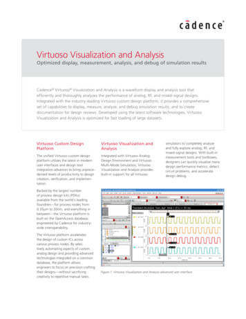
Cadence Virtuoso Logic Gates TutorialA step-by-step description of designing and testing an AND logic gate using Cadence VirtuosoDocument ContentsIntroductionStarting Cadence VirtuosoCreating a Design LibraryCreating a Schematic CellviewCreating a SymbolSetting Up Simulation with Analog Design Environment (ADE)Running Functional Simulations (transient analysis)Appendix A: Saving Image FilesAppendix B: Saving Simulation StatesIntroductionThis document describes how to perform gate-level design and simulation of logic circuits using CadenceVirtuoso with the NCSU design kit. For a full custom design (as opposed to a coded/synthesized design using,e.g., Verilog/VHDL), the design process begins by creating a schematic. The schematic is then simulated toverify operation and optimize performance. To implement an actually microelectronics chip, this would befollowed by creating a layout of the physical circuit, checking for design rule violations, and several other stepsto ensure the design is correct. For ECE331, we will only perform schematic design and simulation of logicgates. In this tutorial you will create a schematic for a basic digital logic gate, and AND gate, and perform somebasic simulations on the schematic to verify it is functioning properly.Starting Cadence VirtuosoBefore beginning this tutorial you should have setup your account to work with Cadence Virtuoso. The stepsfor doing this may vary with each class/project, so be sure to follow any class-specific setup steps beforeproceeding with this tutorial. ECE331 students should have completed the Cadence Virtuoso Setup Guidebefore continuing.Following instructions in the Cadence Virtuoso Setup Guide, start Virtuoso1. With Xming and PuTTY running, move into your Virtuoso working directory (e.g., ECE331/virtuoso) andthen enter the following at the PuTTY command prompt to enable Cadence commands.source SOFT/cadence2. To start Virtuoso (while in ECE331/virtuoso), enter the commandvirtuoso &You should now see two new windows open on your desktop as shown below. The Virtuoso 6.1.3Command/Log (VCL) window will display a log of completed operations and allow you to entercommand-line instruction at the bottom command prompt. When all the configuration files have beenread, you should see a “Done loading NCSU CDK customizations” message in the VCL windowindicating the start up was successful. With each new session, Cadence starts a new CDS.log file inyour working directory where all the messages that appear in the VCL window will be stored.The second window that opens is the Library Manager window, which lists the libraries in your workingdirectory. For ECE331 students, the only library that you will use is the ECE331 library and projectlibraries you create. You can ignore all other libraries; they are for other classes or research purposes.Cadence Virtuoso Logic Gates Tutorialrev: 2013p. 1
Main Virtuoso windows after launching VirtuosoIn this tutorial, a simplified convention will be used to show the sequence of steps for the pull down menu. Forexample, File Exit will indicate that you open the pull down menu for File and then click on Exit. Anotherexample could be Tools Analog Artist Simulation, which will indicate that you pull down the Tools menu,then click on the Analog Artist button and finally click on the Simulation button.Note: If at any time during this tutorial you want to quit Virtuoso, make sure you save your work by selectingFile Save on all open schematics and then close the schematic windows by selecting File Close All.After you have closed all your schematic windows, select File Exit in the VCL window to end the Virtuososession.Creating a Design LibraryCadence File OrganizationTo start a design in Cadence, you must first create a project library where you can store your design cells.Every library is associated with a technology file that supplies the design rules, extraction parameters, etc.required to view, design, and simulate your circuit. Cadence stores its files in libraries, cells, and cellviews.A library (which actually appears as a directory in UNIX) contains cells (subdirectories), which in turn containviews. Each library contains a catalog of all cells, viewed along with the actual UNIX paths to the data files.Each cell in a given library uses the same technology file parameters. A cell is the basic design object. It formsan individual building block of a circuit. It is a logic, rather than a physical, design object. Each cell has one ormore views, which are files that store specific data for each cell. A cellview is the virtual data file created tostore information in Cadence. A cell may have many cellviews, signifying different ways to represent the samedata represented by the cell (for example, a layout, schematic, etc).Example Organization:Library: logic gatesCell: invView: schematicView: symbolCell: nand2View: schematicView: symbolView: layoutView: extractedLibrary: ripple carry adderCell: 1bit adderView: schematicCell: 2bit adderView: schematicCadence Virtuoso Logic Gates Tutorialrev: 2013p. 2
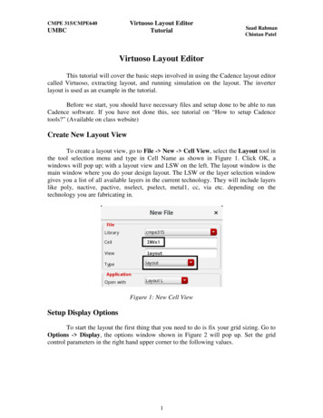
Complete the following steps to create your project library:1. In the Library Manager window, select File New Library to open the New Library window shownbelow.2. Enter a Name for your library. The example shows the library name tutorial, but since you will be usingthe cells in your project library (and adding more to it) choose a name like 331lab, or digital. Do not useECE331 as there is already a parts library with that name. Leave the Path as it defaults. Click OK.3. In the window that opens, click on the Attach to Existing Tech Library button and click OK. Then chooseNCSU TechLib ami06 as the technology file to be associated with your new library. Click OK again.4. Having returned to the New Library window again, click on OK and you will now have an empty projectlibrary you can start adding cells to.New Library windowsCreating a Schematic CellviewComplete the following steps to create the schematic of an AND gate within your new project library.1. Go to the Library Manager window and click/select your library (for example “tutorial”).2. Now select File New Cellview. Use the New File window that pops up to create the schematicview for a 2-input AND gate.3. Make sure your project library is in the Library field. If not, Cancel and repeat step 1. Next, enter theCell Name “2x1AND” for your two-input (and one output) AND gate.4. Select schematic from Type field and Schematic XL from Open with field. This is where you choosewhich Cadence tool you want to use and the appropriate View name for each tool will be filled inautomatically. Here we will be creating the schematic view.5. Click the OK button. The Virtuoso Schematic Editing tool will open with an empty schematic window asshown below.Cadence Virtuoso Logic Gates Tutorialrev: 2013p. 3
New Cell windowsVirtuoso Schematic Editing windowAdd Components: With the 2x1AND cell schematic generated, you can now begin to design the AND gateusing components in the ECE331 library.6. In the Schematic Editing window, select Create Instance to activate the Add Instance tool for addingcomponents (gates, resistors, etc.) to your schematic. You can also invoke this tool by clicking on theInstance icon on the top toolbar (see image below), or by typing the hot key ‘i’ with your mouse over theSchematic Editing window. Two windows (Component Browser window and Add Instance) will popopen.Cadence Virtuoso Logic Gates Tutorialrev: 2013p. 4
Add Instance windows7. If Component Browser window does not appear automatically, select Browse in the Add Instancewindow. In the Component Browser window, under Library select ECE331 (it may be the default). A listof parts will be displayed near the bottom of this window. From the parts list, click on 2x1NAND. Thiswill attach the component to your mouse pointer. You can also type the cell name into the Add Instancewindow (if you know the exact name). If desired, click on the Rotate, Sideways, or Upside-down buttonsin the Add Instance window to manipulate orientation of the component you are adding.8. With the NAND gate selected, click on schematic area (main black area) of the Schematic Editingwindow and the 2x1NAND component will appear in your schematic. Clicking on the schematic windowagain will add another copy of the component, but don’t do this. Pressing ESC on the keyboard willend the Add Instance function, but don’t do this yet either!9. To construct an AND gate out of the gates in the ECE331 library, you will need one NAND gate andone INV gate. Return to the Component Browser window, select the INV cell, and click on theSchematic Editing window to add the INV to your schematic. Place the INV to the right of, but notattached to, the NAND gate since this is where it should go to form an AND function.10. Press ESC to end adding instances.Add Wire Connections: With the gates placed, you can now connect the components to complete the AND.11. In the Schematic Editing window select Create Wire (narrow) (or use hot key ‘w’) to begin placingwires that will connect the terminals of the components and pins in the schematic. Add a wire betweenthe NAND output and the INV input as shown below. Also, add wires on the NAND inputs and INVoutput so that we can place pins on the other end of the wires.When adding wires, click once to start a wire or place a node without ending the wire. To end a wire,double-click or single-clicking on a component terminal (e.g., gate input/output, pin) . Once a wire isended, clicking on the schematic background screen again will start a new wire.12. Press ESC to end wiring. You schematic should now look similar to the schematic below.AND schematic after adding instances and wires.Cadence Virtuoso Logic Gates Tutorialrev: 2013p. 5
Add Pins: All that remains are input and output pins!13. In the Schematic Editing window, select Create Pin (or use hot key ‘p’) to add an input pin.14. In the Add Pin window that opens, enter ‘A’ for the Pin Name and select input for the Direction.15. Click on the Schematic Editing window and drop the pin on the wire to the left of the NAND gate. Clickright on the wire and the pin will be attached to the wire without need to edit the wire or add a new wire.16. Follow the same procedure to an input pin ‘B’ to the other NAND input, and add an output pin ‘Y’ to theoutput of the INV gate. Be sure to select output in the Direction field for the output pin. Note: you canclick on the Rotate, Sideways, or Upside-down buttons in the Add Instance window to manipulateorientation of the component you are adding (not needed here/now).17. Press ‘ESC’ when you a done adding pins.Add Pin window and completed AND schematic.Check and Save the cell view: After completing any schematic, it should be checked for errors and saved.18. To check for errors and save the schematic cell view, click on the Check and Saveicon (blue floppy disk with green check mark). You will be notified if warning or errorswere detected. If so, return to your schematic and look for errors. The most commonerrors are due to improper wiring or forgetting inputs/output pins (unattachedterminals).When everything checks and saves correctly, you will see a message in the VCL window stating“Schematic check completed with no errors” and “ cell name saved”.Creating a SymbolComplete the following steps to create a symbol for your AND gate. A symbol is a simplified representation of acircuit schematic showing only the inputs and outputs. Symbols can be added to other schematics using theAdd Instance tool, just like you added the NAND and INV into your AND schematic. Symbols allow complexcircuits to be represented by simple boxes (or other shapes, like the INV triangle) and I/O pins.1. In the 2x1AND Schematic Editing window select Create Cellview From Cellview.2. Two symbol generation configuration windows will pop up sequentially. Leave all the settings to defaultvalues and select OK in each window to launch the Symbol Editor tool.3. In the Virtuoso Symbol Editing window, notice the default symbol shape is a simple rectangle. Whilethis is functionally fine, it would be better if our AND gate looked like a typical AND symbol. Select theCadence Virtuoso Logic Gates Tutorialrev: 2013p. 6
default green rectangle and delete it. Then, use the drawing tools in the top right menu to draw asymbol closer to an AND gate. Try the Circle and Polygon tools. When you realize these won’t workwell, try the Arc and Line functions.4. Next, use the cursor to move the output (Y) pin to a proper location for you symbol shape. Notice thatthe pin (red box linked to text ‘Y’) is separate from the wire connecting the pin to the symbol body. Youcan move the part and instance identification parameters anywhere that is convenient.Symbol generation windowsDefault (left) and edited (right) AND gate symbol5. When you are happy with your symbol, click the Check and Save icon to, you guessed it, check andsave your symbol. Errors or warning will be noted in the VCL window.6. When your symbol is error free, exit the symbol editor by selecting File Close All.You have now completed the schematic and symbol design portions of this tutorial. Below are some generalediting tips useful for working with Virtuoso and then the tutorial proceeds with simulations, the last (butlengthy) topic.General Editing TipsMouse Buttons: In most Cadence tools, the left mouse button is used to select components, wires, etc., andthe middle mouse button can be used to change object properties, e.g., the width and length of a transistor.Moving Objects: If you want to move any object, just move the cursor on top of the object and type ‘m’. Theobject will then move with the cursor. Or you can select the objects to be moved by left-click and drag todraw a box around the objects. After highlighting the objects to be moved, type ‘m’ and the highlightedobjects will move with your cursor.Deleting Objects: If you want to delete an object, move the cursor on top of the object and hit the ‘DEL’ key.You can also highlight an object or a group of objects by drawing a box around it, as described above, andpressing the ‘DEL’ key.Cadence Virtuoso Logic Gates Tutorialrev: 2013p. 7
Undo Operations: When you make a mistake (accidentally delete a component, etc.), you can undo the actionby click on the Undo icon in the toolbar.BindingKey: The following “hot keys” are available for the schematic editing tool.1). Press ‘p’ to add pins2). Press ‘q’ on the device/instance to edit properties for the device3). Press ‘w’ to add wires4). Press ‘f’ fit the schematic in your schematic window5). Press ‘z’ to zoom in the window6). Press ‘shift z’ to zoom out the window7). Press ‘l’ to label a wire8). Press ‘Up’ and ‘Down’ arrows to move up and down within a schematic window9). Press ‘ESC’ to terminate an operation in the schematic window10). Press ‘u’ to undo an operation in the schematic windowCadence Virtuoso Logic Gates Tutorialrev: 2013p. 8
Setting Up Simulation with Analog Design Environment (ADE)To test the functionality of a schematic we must simulate the circuit. For this task, Cadence provides analogsimulation tools within the Virtuoso Analog Design Environment (ADE). For now we will just run a simpletransient analysis to confirm the circuit designed above is operating as an AND gate should. However, theVirtuoso ADE is capable of running any simulation SPICE can.Setup Analog Simulation:1. With your 2x1AND schematic opened, in the Schematic Editing window select Launch ADE L toopen the Virtuoso Analog Design Environment (ADE) window. You can also launch this tool from theVCL by selecting Tools ADE L Simulation in the VCL menu.2. In the ADE window that opens, choose the cell to be simulated by selecting Setup Design andspecifying the Library Name and Cell Name for your AND gate. Click OK when done.3. Back in the ADE window, click Setup Simulator/Directory/Host. Ensure that spectre is selected asthe Simulator (should be the default). Leave all other settings to default and click OK to exit this setup.Virtuoso ADE window (left) and Setup Simulator window (right).4. In the ADE window, go to Analysis Choose. In the window that opens,make sure the Analysis is set to tran. Enter 10m in the Stop Time inputbox and check Enabled at the bottom. The click OK to save the settings.Setup Stimulus: The schematic defines the components within the cell but doesnot define the control signals (typically voltage sources) necessary to test theoperation of the circuit, such as the power supply voltage and an input voltagesignal. These signals are referred to as the stimulus, and here we will use aspectre stimulus text file to define these signals.You will need to use a text editor in order to create a stimulus text file. You canuse any editor you are familiar with. You can name the stimulus file any name,and put it wherever you wish. In this tutorial, we will call the file “stimulus.txt” and place it in yourECE331/virtuoso directory.5. Start the text editor of your choice. If you are new to UNIX, you may want to use “gedit” by doing thefollowing:oOpen a terminal window (or use any one that is already open). This is a PuTTY window with acommand prompt. If you used the virtuoso & command to launch Virtuoso, you may have to hitENTER to get a command prompt to return.oMake sure you are in your virtuoso directory. If unsure, type cd /ece331/virtuoso.oType gedit & to create a new file.Cadence Virtuoso Logic Gates Tutorialrev: 2013p. 9
6. Once you have opened a text editor, type in the following lines to define the simulator language(spectre), the DC supply voltages, and a two square wave pulse input voltage sources that will allowyou to perform a transient analysis simulation to verify functionality of the AND circuit. Note that theinput waveform used may vary with the type of analysis needed, although the supply voltage source willgenerally remain the same.simulator lang spectreglobal gnd!vdd (vdd! 0) vsource dc 3Gnd (gnd! 0) vsource dc 0V1 (A 0) vsource type pulsewidth 1m period 2mV2 (B 0) vsource type pulsewidth 1m period 3mval0 0val1 3delay 0rise 0.05nfall 0.05nval0 0val1 3delay 0rise 0.05nfall 0.05nNote: Each bulleted item represents one line in your stimulus file. The 5th and 6th lines (V1 and V2 pulsevoltages) are broken into two lines due to the document margins, but they must be on a single line inyour stimulus file.Make sure that you always end the last line by pressing Enter. This adds a new line character to theline, and informs the simulator that the voltage definition is complete. If you do not do this, you willlikely get a netlist read error when you try to Netlist and Run the simulation.7. Save the text file. If you are using gedit, this can be done by selecting File Save As , entering a‘Name’ like stimulus.txt, choosing the path to /ECE331/virtuoso in the ‘Save in folder’ area, and clickingSave at the bottom.8. You can exit the text editor. For gedit, use File Quit. However, you may want to keep the editor opento work on other simulation stimulus files later.If you have any trouble creating your own stimulus file, you can download a file with the same values as abovefrom the class website. Choose Lab1A.txt and save it to your virtuoso directory. Note, the tutorial will assumethe file is saved as “stimulus.txt”.Regarding the Stimulus FileThe voltage sources above are defined using spectre syntax. The DC supply voltage named “vdd” is betweennodes vdd! and 0 (ground) with value of 3V. The input square wave is defined using the spectre pulse syntax vname (node node-) vsource type pulse val0 not pulse voltage val1 pulse voltagedelay delay length rise rise time fall fall time width pulse width period period lengthwhere the default units are volts and seconds. The ‘n’ on the time values sets them to nanoseconds (i.e. ‘n’ isa 10-9 multiplier). Although you can vary the timing values as necessary to meet simulation goals, the rise andfall times shown in Step 6 are good for the chosen CMOS technology and should not be modified unless youare sure you know what you are doing. The illustration below helps to define the pulse waveform parameters.Illustration of pulse waveform parameters (left) and two example pulse definitions (right)Cadence Virtuoso Logic Gates Tutorialrev: 2013p. 10
Linking Stimulus File:9. Once you have saved the stimulus file, return to the ADE window and link your stimulus file to thesimulation program. Click on Setup Simulation Files.10. In the setup window that opens, you need to locate your stimulus file. Below the line “Stimulus Files”,click on the “ Click here to add a file ” line and a Browse button should appear on the right hand side.Click the Browse button, select your stimulus file from the window that opens, and click Open to returnto the setup window. You should now see the absolute pathname for your stimulus file listed under“Stimulus Files”. If so, click OK to close the setup window without changing anything else.Simulation Files Setup windowSetup Output Traces: The only step that remainsbefore running the simulation is to select what signalsyou would like to view after the simulation iscomplete.11. In the ADE window, select Outputs To BePlotted Select On Schematic. This willactivate the Schematic Editor window andallow you to pick the signals (nets/wires) youwould like to have plotted during thesimulation simply by clicking on them.12. In the Schematic Editor window, click on thewire that is connected to the output (Y) of theAND gate. Then, select (click on) the wiresconnected to each of the inputs (A and B). As you click, you should see the signals being added to theADE window.This completes your simulation setup. Your ADE window should now look like the image on the right.Running Functional Simulations (transient analysis)Now you will verify that the circuit you designed is indeed operating like and AND gate.Running the Simulation:1. In the ADE window, select Simulation Netlist and Run to start the simulation using all of theparameters you just setup. When the simulation is complete, the VCL log should show "readingsimulation data . successful" (although there may be lines after this too). If the simulation was notsuccessful, go to Simulation Output Log in the ADE window to find out what the problem was.2. The simulation results will be plotted in a waveform window. Initially, all plotted signals will appear ontop of each other. To separate the signals, select Axis Strips in the waveform window.Cadence Virtuoso Logic Gates Tutorialrev: 2013p. 11
3. Under Part 1 of the Lab 1 Check-off Sheet, enter the expected output values (0 or 1) in the Theoreticalcolumn for each input combination of an AND gate. Hint: only one of the rows should be ‘1’! :D4. Now, view the plotted signals in the waveform window. Observe the output value (0 or 1) for each A,Binput combination (0, 0), etc. Note: the inputs will not be in the save order as the truth table. Verify thesimulation results match the expected/theoretical values. If not, look back at your circuit schematic andtry to determine what is wrong. Re-run simulations until you get the proper response. Consult the TA ifyou need help.Simulation waveform window (with slightly different stimulus pattern than defined above)5. When your AND gate is simulating correctly, show the TA your schematic, symbol, and simulationresults. Ask the TA to sign off on Part 1 of your Check-off Sheet.6. To close all Virtuoso windows, it is best to close them individually to ensure everything has been saved.Close the ADE by selecting Session Quit. Close the Schematic Editing window by clicking File Close (or Close All). To complete the rest the lab assignment you may not want to close the main VCLwindow yet, but when you do simply select File Exit. You will then need to type “exit” into the PuTTYcommand prompt for each terminal you have logged into (until the PuTTY window closes).You have now completed the tutorial and can continue with the next step of your lab assignment. Pleasenote, the following appendix provides valuable information regarding saving images (of schematics, simulationplots, etc.). You will need to perform this task later. You can either try it now for practice or refer to this tutorialin later labs when these steps are required. A second appendix provides instruction on saving and loadingsimulation states that might save you some time in the future. Just remember that this information is in thistutorial.Cadence Virtuoso Logic Gates Tutorialrev: 2013p. 12
Appendix A: Saving Image FilesIn order to more clearly see plot results, the graph text can be made larger and plot lines can be made thicker. To make the plot line thicker, in the Waveform Window , select each signal trace (individually) then rightclick on the selected line and choosing Edit. The options in the Trace Attributes window are shownbelow and are self explanatory. Try changing all traces to Solid and Bold style. To make the text on the graph larger, in the Waveform Window select on (for example) Graph Font Extra Large.Adjusting waveform display parametersIn order to save a graph or schematic as an image file, for example to include within a report, follow the stepsbelow. In the Waveform Window click on File Save as Image. In the configuration window that opens, youcan set the image type (PNG, TIFF, or BMP), choose to convert the black background to white, andchoose a filename to save to. The image file will be saved in your current working directory (from whichyou initially launched Virtuoso) unless you browse to a new location. To save a schematic as an image file, in the SchematicEditing window select File Export Image. Theconfiguration window to the right will open. Enter in thename at the top of the window, select the image type(PNG by default) and select the Background to beTransparent (generally preferred over a blackbackground). Click Export and the image will be saved inyour virtuoso working directory.Cadence Virtuoso Logic Gates Tutorialrev: 2013p. 13
Appendix B: Saving Simulation StatesAnalog Design Environment states can be saved so that the settings do not need to be manually entered eachtime a design is simulated. However, the default settings can consume a lot of disc space so be sure you studyyour options a bit and monitor your disc usage if you choose to use this feature. To save the simulation state, in the Analog Design Environment window select Session Save State.The “Save As” field does not have to be a unique name for all designs; the state is saved within thedirectory of the current cellview. Thus, you can use the same Save As name for multiple cells withoutoverwriting each other. For example, cells named inv and nand2 can both independently have thestate “state1” saved. Enter a Save As name, e.g., “state1” and click on OK. Note, by default the states will be saved at yourroot directory in a folder titled “.artist states”. Saving all simulation data can take a lot of memory so you may find it useful to alter the What to Saveparameters to save only the items you need to run future simulations. Saving outputs from complexcells with multiple plotted node waveforms can generate very large (GB!) files. A good starting pointwould be to save only the parameters that were set during this tutorial, such as Analyses, Model Setup,Simulator Options, and Stimulation Files. To load the saved state, after opening a specific cell, in the Analog Design Environment window selectSession Load State. Select the desired State Name and click on OK.Save (left) and load (right) simulation states windowsTHE ENDCadence Virtuoso Logic Gates Tutorialrev: 2013p. 14
To check for errors and save the schematic cell view, click on the Check and Save icon (blue floppy disk with green check mark). You will be notified if warning or errors were detected. If so, return to your schematic and look for errors. The most common errors are due to improper wiring or forgetting inputs/output pins (unattached terminals).